2928wifi规格书
MEMORY存储芯片MT29F4G08ABADAWP-ITD中文规格书

NAND Flash MemoryMT29F4G08ABADAH4, MT29F4G08ABADAWP, MT29F4G08ABBDAH4, MT29F4G08ABBDAHC, MT29F4G16ABADAH4, MT29F4G16ABADAWP, MT29F4G16ABBDAH4, MT29F4G16ABBDAHC, MT29F8G08ADADAH4,MT29F8G08ADBDAH4, MT29F8G16ADADAH4, MT29F8G16ADBDAH4, MT29F16G08AJADAWPFeatures•Open NAND Flash Interface (ONFI) 1.0-compliant1•Single-level cell (SLC) technology •Organization–Page size x8: 2112 bytes (2048 + 64 bytes)–Page size x16: 1056 words (1024 + 32 words)–Block size: 64 pages (128K + 4K bytes)–Plane size: 2 planes x 2048 blocks per plane–Device size: 4Gb: 4096 blocks; 8Gb: 8192 blocks 16Gb: 16,384 blocks•Asynchronous I/O performance–t RC/t WC: 20ns (3.3V), 25ns (1.8V)•Array performance–Read page: 25µs 3–Program page: 200µs (TYP: 1.8V, 3.3V)3–Erase block: 700µs (TYP)•Command set: ONFI NAND Flash Protocol •Advanced command set–Program page cache mode4–Read page cache mode 4–One-time programmable (OTP) mode–Two-plane commands 4–Interleaved die (LUN) operations–Read unique ID–Block lock (1.8V only)–Internal data move•Operation status byte provides software method for detecting–Operation completion–Pass/fail condition–Write-protect status•Ready/Busy# (R/B#) signal provides a hardware method of detecting operation completion•WP# signal: Write protect entire device •First block (block address 00h) is valid when ship-ped from factory with ECC. For minimum required ECC, see Error Management.•Block 0 requires 1-bit ECC if PROGRAM/ERASE cy-cles are less than 1000•RESET (FFh) required as first command after pow-er-on•Alternate method of device initialization (Nand_In-it) after power up (contact factory)•Internal data move operations supported within the plane from which data is read•Quality and reliability–Data retention: 10 years–Endurance: 100,000 PROGRAM/ERASE cycles •Operating voltage range–V CC: 2.7–3.6V–V CC: 1.7–1.95V•Operating temperature:–Commercial: 0°C to +70°C–Industrial (IT): –40ºC to +85ºC•Package–48-pin TSOP type 1, CPL2–63-ball VFBGANotes: 1.The ONFI 1.0 specification is available at2.CPL = Center parting line.3.See Program and Erase Characteristics fort R_ECC and t PROG_ECC specifications.4.These commands supported only with ECCdisabled.Figure 78: TWO-PLANE BLOCK ERASERE#CE#ALECLE I/Ox R/B#WE#Figure 79: TWO-PLANE/MULTIPLE-DIE READ STATUS CycleCE#CLE ALE RE#I/Ox4Gb, 8Gb, 16Gb: x8, x16 NAND Flash MemoryTwo-Plane OperationsInterleaved Die (Multi-LUN) OperationsIn devices that have more than one die (LUN) per target, it is possible to improve per-formance by interleaving operations between the die (LUNs). An interleaved die (multi-LUN) operation is one that is issued to an idle die (LUN) (RDY = 1) while another die (LUN) is busy (RDY = 0).Interleaved die (multi-LUN) operations are prohibited following RESET (FFh), identifi-cation (90h, ECh, EDh), and configuration (EEh, EFh) operations until ARDY =1 for all of the die (LUNs) on the target.During an interleaved die (multi-LUN) operation, there are two methods to determine operation completion. The R/B# signal indicates when all of the die (LUNs) have finish-ed their operations. R/B# remains LOW while any die (LUN) is busy. When R/B# goes HIGH, all of the die (LUNs) are idle and the operations are complete. Alternatively, the READ STATUS ENHANCED (78h) command can report the status of each die (LUN) in-dividually.If a die (LUN) is performing a cache operation, like PROGRAM PAGE CACHE (80h-15h),then the die (LUN) is able to accept the data for another cache operation when status register bit 6 is 1. All operations, including cache operations, are complete on a die when status register bit 5 is 1.During and following interleaved die (multi-LUN) operations, the READ STATUS (70h)command is prohibited. Instead, use the READ STATUS ENHANCED (78h) command to monitor status. This command selects which die (LUN) will report status. When two-plane commands are used with interleaved die (multi-LUN) operations, the two-plane commands must also meet the requirements in Two-Plane Operations.See Command Definitions for the list of commands that can be issued while other die (LUNs) are busy.During an interleaved die (multi-LUN) operation that involves a PROGRAM series (80h-10h, 80h-15h) operation and a READ operation, the PROGRAM series operation must be issued before the READ series operation. The data from the READ series opera-tion must be output to the host before the next PROGRAM series operation is issued.This is because the 80h command clears the cache register contents of all cache regis-ters on all planes.4Gb, 8Gb, 16Gb: x8, x16 NAND Flash MemoryInterleaved Die (Multi-LUN) OperationsError ManagementEach NAND Flash die (LUN) is specified to have a minimum number of valid blocks(NVB) of the total available blocks. This means the die (LUNs) could have blocks thatare invalid when shipped from the factory. An invalid block is one that contains at leastone page that has more bad bits than can be corrected by the minimum required ECC.Additional blocks can develop with use. However, the total number of available blocksper die (LUN) will not fall below NVB during the endurance life of the product.Although NAND Flash memory devices could contain bad blocks, they can be usedquite reliably in systems that provide bad block management and error-correction algo-rithms. This type of software environment ensures data integrity.Internal circuitry isolates each block from other blocks, so the presence of a bad blockdoes not affect the operation of the rest of the NAND Flash array.NAND Flash devices are shipped from the factory erased. The factory identifies invalidblocks before shipping by attempting to program the bad block mark into every loca-tion in the first page of each invalid block. It may not be possible to program every loca-tion with the bad block mark. However, the first spare area location in each bad block isguaranteed to contain the bad block mark. This method is compliant with ONFI FactoryDefect Mapping requirements. See the following table for the first spare area locationand the bad block mark.System software should check the first spare area location on the first page of eachblock prior to performing any PROGRAM or ERASE operations on the NAND Flash de-vice. A bad block table can then be created, enabling system software to map aroundthese areas. Factory testing is performed under worst-case conditions. Because invalidblocks could be marginal, it may not be possible to recover this information if the blockis erased.Over time, some memory locations may fail to program or erase properly. In order toensure that data is stored properly over the life of the NAND Flash device, the followingprecautions are required:•Always check status after a PROGRAM or ERASE operation•Under typical conditions, use the minimum required ECC (see table below)•Use bad block management and wear-leveling algorithmsThe first block (physical block address 00h) for each CE# is guaranteed to be validwith ECC when shipped from the factory.Table 21: Error Management DetailsTable 21: Error Management Details (Continued)。
3028技术参数

固定端口 管理端口24 个 10/100Base-T 以太网端口 4 个 1000Base-X SFP 端口 1 个 Console 口 AC 电源电源额定电压范围:120V~240V ;50/60Hz 额定电压范围:100V~265V ;50/60Hz最大功耗 体系结构 交换容量 包转发率 交换模式 广播控制22W 基于高性能 ASIC 芯片技术 12.8Gbps 9.6Mpps 存储转发(Store and Forward) 支持抑制广播风暴,达到临界点时即停止发送 支持 IEEE802.3x 流控(全双工)端口特性基于端口速率百分比的广播, DLF , 组播风暴抑制 基于端口 pps 的广播风暴抑制 ; 支持 8KMAC 地址表容量MAC 地址支持 MAC 地址过滤 支持手工配置老化时间 支持静态 MAC 地址配置 支持手工聚合 支持基于源 MAC/目的 MAC 负载均衡端口汇聚支持静态/动态 LACP 最大支持 4 个聚合组 FE 汇聚组最大支持 8 个 FE 接口 支持基于端口的 VLAN(4K 个)VLAN 特性三层 VLAN 数量 1 个 支持 VLAN 过滤 支持 PVLAN DHCP ServerDHCPDHCP Snooping DHCP Relay 支持无状态地址自动配置 支持重复地址检测 (DAD)IPv6 协议支持邻居发现 (ND) 支持 ICMPv6 支持路由器发现生成树协议 组播支持 STP,RSTP,MSTP 支持 IGMP Snooping,MLD snooping, 支持未知组播丢弃功能 支持 N:1 端口镜像 支持数据流镜像镜像支持本地端口镜像(LSPAN) 支持基于 VLAN、ACL、端口的镜像(LSPAN) 支持远程端口镜像(RSPAN)支持 rate-limit 对物理接口 output 双向方向限速 支持基于源 MAC 地址、目的 MAC 地址、源 IP 地址、目的 IP 地址和源端口、目的端口的分流 支持基于协议号、802.1p、IP Precedence、DSCP Input interface 的分流 支持 TOS/DSCP 标记 支持报文的 802.1p、IP Precedence、DSCP 重新标记 支持 CAR 限速 QoS 支持报文重定向 支持基于 Police 的限速 支持基于 CLASS-MAP 的限速 支持流量整形 每端口的输出队列数量最大 8 个 支持丰富的端口队列调度模式 支持基于源 MAC 地址、目的 MAC 地址 ACL 支持基于源 IP 地址、目的 IP 地址 ACL 支持基于源端口、目的端口 ACL 支持基于协议号 ACL 支持基于 VLAN 的 ACL ACL 支持基于时间段(Time Range)的 ACL 支持基于支持非法帧过滤 支持在 Ingress 方向和 Egress 方向的 ACL 加载 支持基于 VLAN 加载 ACL 支持基于 Switch port 加载 ACL 用户分级管理和口令保护 SSH2.0 支持 IEEE802.1x 认证,在未认证前可访问指定的网络 支持 MAC 自动学习绑定并可手动设置端口 MAC 学习绑定的个数 支持动态 arp 检测(DAI: Dynamic ARP Inspection),Dhcp 报文检测,Nd 报文检测 基于 DHCP-Snooping 的 ARP 攻击防御 Dhcpv6 报文检测 支持 TCP 并发连接数限制(CP) 安全特性 MAC+IP+PORT 绑定(自动/手动) MAC+IP+PORT+VLAN 绑定(自动/手动) 支持 IEEE 802.1X 认证、AAA 认证、Radius 认证 支持 TCP SYN Flood 攻击防御 支持授权用户 telnet 登录管理 支持端口隔离 支持定向广播转发抑制功能 支持带源路由选项报文转发抑制功能 支持 MSTP BPDU Guard、Loop Guard、Root Guard、PBDU Skewing 功能 支持 WindROSE 图形化网管系统 支持 FTP/ TFTP 加载升级和 Xmodem 加载升级 管理与维护 支持命令行接口(CLI),Telnet,Console 口配置 RMON 网管 支持网络诊断命令:PING、 支持 SNMP v1/v2、SNMP v3 支持 NTP 客户端和服务器端支持 NTP 协议 支持 RMON (Remote Monitoring)1,2,3,9 组 MIB 本地 SYSlog:系统日志,分级告警,调试配置信息输出 远程 SYSlog:系统日志,分级告警,调试配置信息输出电源 功耗 液晶面板 液晶板尺寸 显示方式 显示器像素 镜头100-240V 交流电,50/60Hz 365W(节能待机模式 下为 0.3W,普通待机模式下为 11.5W)*116.0mm(0.63 英寸)对角线(4:3 宽高比) 透射式液晶面板(×3, R/G/B) 786,432(1,024x768)x 3, 共计 2,359,296 像素 手动 1.6 倍变焦(1.18-1.90:1), 手动对焦 F 1.60–2.12, f 15.30–24.64mm灯泡280W x 1, 灯泡更换周期(灯泡功率:普通/节能模式):2,500 小时/4.000 小时*2投影画面尺寸(对 0.76-7.62m(30-300 英寸),4:3 宽高比 角线) 亮度*35,000 流明(灯泡功率:普通模式)*3均匀性 对比度 分辨率85% 4,000:1(全开/全关,灯泡功率:自动模式,lris:开) 1,024×768 像素*4*3扫描频率 HDMI RGB(模拟) fH: 25-80 kHz,fV: 50-85 Hz,点时钟:162 MHz 或更低 fH: 15-100 kHz, fV: 50-100 Hz, 点时钟:140 MHz 或更低 (信号超出 140 MHz 点时钟率时重采样) YPBPR(YCBCR) fH: 15.75 kHz, fV: 60 Hz [480i(525i)] fH: 15.63 kHz, fV: 50 Hz [576i(625i)] fH: 31.50 kHz, fV: 60 Hz [480p(525p)] fH: 31.25 kHz, fV: 50 Hz [576p(625p)] fH: 45.00 kHz, fV: 60 Hz [720(750)/60p] fH: 37.50 kHz, fV: 50 Hz [720(750)/50p] fH: 33.75 kHz, fV: 60 Hz [1080(1125)/60i] fH: 28.13 kHz, fV: 50 Hz [1080(1125)/50i] 视频/S-视频 fH: 15.75 kHz,fV: 60 Hz [NTSC/NTSC4.43/PAL-M/PAL60], fH: 15.63 kHz, fV: 50 Hz [PAL/PAL-N/SECAM] 光轴移动范围 梯形校正范围(约) 安装方式 终端接口 HDMI 输入 HDMI 19-pin × 1(兼容 HDCP) 480p, 576p, 720/60p, 720/50p, 1080/60i, 1080/50i, 1080/60p, 1080/50p, VGA (640 x 480)-WUXGA (1,920 x 1,200)*5, 只与逐行信号兼容, 点时钟: 25 -146.25 MHz 电脑 1 输入 D-Sub HD 15-pin(雌头) × 1(RGB/YPBPR/YCBCR × 1) 垂直:+40% 垂直:± (梯形校正范围内为± ) 30° 20° 吊装/平放,正投/背投电脑 2 输入/输出 D-Sub HD 15-pin(雌头) × 1(RGB × 1)(使用屏幕上的菜单选择输入/输出) (当电脑 2 选择监控器输出时, 输出的信号是电脑 1 输入的信号) 视频输入 S-视频输入 音频输入 RCA × 1(复合视频) Mini DIN 4-pin × 1(S-视频) RCA pin x 2(L-R x 1)用于视频/S-视频输入电脑音频输入 1 M3(L, R) × 1 电脑音频输入 2 M3(L, R) × 1, 为音频输入或麦克风连接用(可变) (麦克风输入) 音频输出 串行输入 局域网 内置扬声器 噪音水平 机身材料 尺寸(宽×高×长) 重量 运行环境 随机附件 M3 x 1(L-R x 1) 为输出用(可变) D-sub 9-pin(雌头) × 1, 用于外部控制(与 RS-232C 相容) RJ-45x1(网络连接用, 10Base-T/100Base-TX, 适用于 PJ Link ) 4 cm 圆形 x 1, 输出功率: 10W(单声道) 37dB(灯泡功率: 普通模式), 29dB(灯泡功率: 节能模式) 树脂成型品 379x107x305mm(含支撑脚最短, 不包含凸出部分) 约 4.8 kg 运行温度: 0° C–40° C*6, 运行湿度: 20%-80%(无结霜) 电源线 x 1, 电源线固定支架 x 1, 无线遥控器, 遥控器电池(AAA/R03/LR03 type x 2), 携带软包 x 1,RGB 电缆(1.8 m, 用于 VGA) x 1, 软件 CD-ROM(Logo 传送软件, 多台投影机监控软件)TM产品型号 单元组成 额定阻抗 额定功率 最大功率 频响范围 灵敏度 净重 毛重OT55 5 " x 5 80 hms 250 W 450 W 100 Hz - 150 KHz 92 dB±3dB 8 kg / pair 10 kg / pair基本规格产品类型:超 5 类双绞线网络 产品适用:布线网络 最大单段长度:100 米 纠错 传输速率:1000Mbps 包装长度:305 米外观参数 产品特性 产品特性 1:提供基于 100MHZ 带宽环境下的数据传输支持 Ethernet 和快速 Ethern 622Mbps 的 ATM. 符合 CSA,ETL,经 UL 认证主要规格 类型:网络服务器机柜 容量:42U标准:符合 ANSI/EIA RS-310-D、IEC297-2、DIN41491;PART1、DIN41494;P GB/T3047.2-92 标准;兼容 ETSI 标准门及门锁:高通风率六角弧形网孔前门(专利)、双开六角网孔后门及三段侧门;月光 门锁 纠错材料及工艺:SPCC 优质冷扎钢板制作;厚度:方孔条 2.0mm,托盘 2.0mm,安装 其他 1.2mm;表面处理:脱脂、酸洗、磷化、静电喷塑附加功能:外观高贵典雅,工艺精湛、尺寸精密,媲美国际最高档网络服务器机柜, 机房工程形象;可方便地安装图腾机柜集中配电单元(专利)外观参数 高度:1999mm 宽度:600mm 深度:1000mm型号 产品类型 线材 干扰功能 主要参数超 5 类 24 口配线架(0-0406330-1)有奖找错 线架 超5类 非屏蔽型 非屏蔽超 5 类 24 口配线架基本参数 固定端口 管理端口 电源 最大功耗 体系结构 交换容量 包转发率 交换模式 广播控制 端口特性 24 个 10/100Base-T 以太网端口 4 个 1000Base-X SFP 端口 1 个 Console 口 AC 电源 额定电压范围:120V~240V ;50/60Hz 额定电压范围:100V~265V ;50/60Hz 22W 基于高性能 ASIC 芯片技术 12.8Gbps 9.6Mpps 存储转发(Store and Forward) 支持抑制广播风暴,达到临界点时即停止发送 支持 IEEE802.3x 流控(全双工) 基于端口速率百分比的广播, DLF , 组播风暴抑制 基于端口 pps 的广播风暴抑制 ; 支持 8KMAC 地址表容量 支持 MAC 地址过滤 支持手工配置老化时间 支持静态 MAC 地址配置 支持手工聚合 支持基于源 MAC/目的 MAC 负载均衡 支持静态/动态 LACP 最大支持 4 个聚合组 FE 汇聚组最大支持 8 个 FE 接口 支持基于端口的 VLAN(4K 个) 三层 VLAN 数量 1 个 支持 VLAN 过滤 支持 PVLAN DHCP Server DHCP Snooping DHCP Relay 支持无状态地址自动配置 支持重复地址检测 (DAD) 支持邻居发现 (ND) 支持 ICMPv6 支持路由器发现 支持 IGMP Snooping,MLD snooping, 支持未知组播丢弃功能 支持 N:1 端口镜像 支持数据流镜像 支持本地端口镜像(LSPAN) 支持基于 VLAN、ACL、端口的镜像(LSPAN)MAC 地址端口汇聚VLAN 特性DHCPIPv6 协议生成树协议 支持 STP,RSTP,MSTP 组播镜像支持远程端口镜像(RSPAN) 支持 rate-limit 对物理接口 output 双向方向限速 支持基于源 MAC 地址、目的 MAC 地址、源 IP 地址、目的 IP 地址和源端口、 目的端口的分流 支持基于协议号、802.1p、IP Precedence、DSCP Input interface 的分流 支持 TOS/DSCP 标记 支持报文的 802.1p、IP Precedence、DSCP 重新标记 支持 CAR 限速 支持报文重定向 支持基于 Police 的限速 支持基于 CLASS-MAP 的限速 支持流量整形 每端口的输出队列数量最大 8 个 支持丰富的端口队列调度模式 支持基于源 MAC 地址、目的 MAC 地址 ACL 支持基于源 IP 地址、目的 IP 地址 ACL 支持基于源端口、目的端口 ACL 支持基于协议号 ACL 支持基于 VLAN 的 ACL 支持基于时间段(Time Range)的 ACL 支持基于支持非法帧过滤 支持在 Ingress 方向和 Egress 方向的 ACL 加载 支持基于 VLAN 加载 ACL 支持基于 Switch port 加载 ACL 用户分级管理和口令保护 SSH2.0 支持 IEEE802.1x 认证,在未认证前可访问指定的网络 支持 MAC 自动学习绑定并可手动设置端口 MAC 学习绑定的个数 支持动态 arp 检测(DAI: Dynamic ARP Inspection),Dhcp 报文检测,Nd 报 文检测 基于 DHCP-Snooping 的 ARP 攻击防御 Dhcpv6 报文检测 支持 TCP 并发连接数限制(CP) MAC+IP+PORT 绑定(自动/手动) MAC+IP+PORT+VLAN 绑定(自动/手动) 支持 IEEE 802.1X 认证、AAA 认证、Radius 认证 支持 TCP SYN Flood 攻击防御 支持授权用户 telnet 登录管理 支持端口隔离 支持定向广播转发抑制功能 支持带源路由选项报文转发抑制功能 支持 MSTP BPDU Guard、Loop Guard、Root Guard、PBDU Skewing 功能QoSACL安全特性支持 WindROSE 图形化网管系统 管理与维护 支持 FTP/ TFTP 加载升级和 Xmodem 加载升级 支持命令行接口(CLI),Telnet,Console 口配置 RMON 网管支持网络诊断命令:PING、 支持 SNMP v1/v2、SNMP v3 支持 NTP 客户端和服务器端 支持 NTP 协议 支持 RMON (Remote Monitoring)1,2,3,9 组 MIB 本地 SYSlog:系统日志,分级告警,调试配置信息输出 远程 SYSlog:系统日志,分级告警,调试配置信息输出基本参数 电源 功耗 液晶板尺寸 显示方式 显示器像素 镜头 100-240V 交流电,50/60Hz 365W(节能待机模式 下为 0.3W,普通待机模式下为 11.5W) 16.0mm(0.63 英寸)对角线(4:3 宽高比) 透射式液晶面板(×3, R/G/B) 786,432(1,024x768)x 3, 共计 2,359,296 像素 手动 1.6 倍变焦(1.18-1.90:1), 手动对焦 F 1.60–2.12, f 15.30–24.64mm 280W x 1, 灯泡更换周期(灯泡功率:普通/节能模式):2,500 小时/4.000 小时 0.76-7.62m(30-300 英寸),4:3 宽高比 5,000 流明(灯泡功率:普通模式)*3 *2 *1灯泡 投影画面尺寸 亮度*3均匀性 对比度 分辨率85% 4,000:1(全开/全关,灯泡功率:自动模式,lris:开) 1,024×768 像素*4 fH: 25-80 kHz,fV: 50-85 Hz,点时钟:162 MHz 或更低 fH: 15-100 kHz, fV: 50-100 Hz, 点时钟:140 MHz 或更低 (信号超出 140 MHz 点时钟率时重采样) fH: 15.75 kHz, fV: 60 Hz [480i(525i)] fH: 15.63 kHz, fV: 50 Hz [576i(625i)]*3HDMI RGB(模拟)YPBPR(YCBCR)fH: 31.50 kHz, fV: 60 Hz [480p(525p)] fH: 31.25 kHz, fV: 50 Hz [576p(625p)] fH: 45.00 kHz, fV: 60 Hz [720(750)/60p] fH: 37.50 kHz, fV: 50 Hz [720(750)/50p] fH: 33.75 kHz, fV: 60 Hz [1080(1125)/60i] fH: 28.13 kHz, fV: 50 Hz [1080(1125)/50i]视频/S-视频 光轴移动范围 梯形校正范围(约) 安装方式 终端接口 HDMI 输入fH: 15.75 kHz,fV: 60 Hz [NTSC/NTSC4.43/PAL-M/PAL60], fH: 15.63 kHz, fV: 50 Hz [PAL/PAL-N/SECAM] 垂直:+40% 垂直:± (梯形校正范围内为± ) 30° 20° 吊装/平放,正投/背投HDMI 19-pin × 1(兼容 HDCP)480p, 576p, 720/60p, 720/50p, 1080/60i, 1080/50i, 1080/60p, 1080/50p, VGA (640 x 480)-WUXGA (1,920 x 1,200)*5, 只与逐行信号兼容, 点时钟: 25 -146.25 MHz 电脑 1 输入 电脑 2 输入/输出 视频输入 S-视频输入 音频输入 电脑音频输入 1 电脑音频输入 2 (麦克风输入) 音频输出 串行输入 局域网 内置扬声器 噪音水平 机身材料 尺寸(宽×高×长) 重量 运行环境 D-Sub HD 15-pin(雌头) × 1(RGB/YPBPR/YCBCR × 1) D-Sub HD 15-pin(雌头) × 1(RGB × 1)(使用屏幕上的菜单选择输入/输出) (当电脑 2 选择监控器输出时, 输出的信号是电脑 1 输入的信号) RCA × 1(复合视频) Mini DIN 4-pin × 1(S-视频) RCA pin x 2(L-R x 1)用于视频/S-视频输入 M3(L, R) × 1 M3(L, R) × 1, 为音频输入或麦克风连接用(可变) M3 x 1(L-R x 1) 为输出用(可变) D-sub 9-pin(雌头) × 1, 用于外部控制(与 RS-232C 相容) RJ-45x1(网络连接用, 10Base-T/100Base-TX, 适用于 PJ Link ) 4 cm 圆形 x 1, 输出功率: 10W(单声道) 37dB(灯泡功率: 普通模式), 29dB(灯泡功率: 节能模式) 树脂成型品 379x107x305mm(含支撑脚最短, 不包含凸出部分) 约 4.8 kg 运行温度: 0° C–40° C*6, 运行湿度: 20%-80%(无结霜) 电源线 x 1, 电源线固定支架 x 1, 无线遥控器, 遥控器电池(AAA/R03/LR03 type x 随机附件 2), 携带软包 x 1,RGB 电缆(1.8 m, 用于 VGA) x 1, 软件 CD-ROM(Logo 传送软件, 多 台投影机监控软件) 基本参数 单元组成 额定阻抗 额定功率 最大功率 频响范围 灵敏度 净重 5 " x 5 80 hms 150 W 350 W 100 Hz - 150 KHz 92 dB±3dB 8 kg / pairTM。
2928系列教育专用交换机

产品简介Cisco ® Catalyst ® 2928系列教育专用交换机Cisco ® Catalyst ® 2928系列交换机,是为中国校园网络定制的高安全和高性价比的二层百兆接入交换机。
该系列采用以太网供电 (Power Over Ethernet – PoE) 或非PoE 配置,可提供桌面快速以太网连接,可为校园网接入提供统一的有线和无线安全解决方案。
Catalyst 2928系列采用先进的硬件和软件技术,并结合第三方的认证管理系统,实现基于身份的网络部署,大幅度提高校园网络的安全。
简单易行的认证模式,自由定制化的认证界面,高度集成的安全特性,性能卓越的系统硬件,稳定可靠的软件和高性价比,这些都将使Catalyst 2928成为校园网接入交换机的理想选择。
Cisco Catalyst 2928软件镜像是一组丰富的智能服务,包括高级认证 、ACL 和IPv4管理。
基于SFP 的千兆以太网端口可兼容多种不同的SFP 模块。
以下是Catalyst 2928 各种型号Catalyst 2928系列交换机所能提供给校园网用户的主要特点:• 有线无线统一解决方案在统一的上层管理软件平台上,有线与无线进行一致的认证,结合第三方的软件实现完整的安 全解决方案• 强大的安全特性可实现用户特征的7元素组合绑定,最大限度的保证网络的接入侧安全一键式安全开启实现ARP 防御,DHCP 欺骗,端口安全等安全防御策略 • 创新的认证方式基于WEB 的终端认证模式,实现跨平台跨浏览器的接入认证,同时提供可定制化的认证界面,保证信息的准确传递 • 中国化的产品专为中国教育行业定制的交换机,无论是面板还是管理界面都采用中文描述,大大缩短用户用户熟悉设备的时间有线无线统一的安全解决方案该方案使用catalyst 2928交换机的独特特性再加上第三方的上层管理软件将为安全校园网的建设提供安全,可靠,易用的整体解决方案。
MEMORY存储芯片MT29F8G08ABABAWP-ITB中文规格书

Status OperationsEach die (LUN) provides its status independently of other die (LUNs) on the same targetthrough its 8-bit status register.After the READ STATUS (70h) or READ STATUS ENHANCED (78h) command is issued,status register output is enabled. The contents of the status register are returned on I/O[7:0] for each data output request.When the asynchronous interface is active and status register output is enabled,changes in the status register are seen on I/O[7:0] as long as CE# and RE# are LOW; it isnot necessary to toggle RE# to see the status register update.While monitoring the status register to determine when a data transfer from the Flasharray to the data register (t R) is complete, the host must issue the READ MODE (00h)command to disable the status register and enable data output (see Read Operations).The READ STATUS (70h) command returns the status of the most recently selected die(LUN). To prevent data contention during or following an interleaved die (multi-LUN)operation, the host must enable only one die (LUN) for status output by using the READSTATUS ENHANCED (78h) command (see Interleaved Die (Multi-LUN) Operations).With internal ECC enabled, a READ STATUS command is required after completion ofthe data transfer (t R_ECC) to determine whether an uncorrectable read error occurred. Table 18: Status Register DefinitionNotes: 1.Status register bit 6 is 1 when the cache is ready to accept new data. R/B# follows bit 6.Read OperationsThe READ PAGE (00h-30h) command, when issued by itself, reads one page from theNAND Flash array to its cache register and enables data output for that cache register.During data output the following commands can be used to read and modify the data inthe cache registers: RANDOM DATA READ (05h-E0h) and RANDOM DATA INPUT (85h).Read Cache OperationsTo increase data throughput, the READ PAGE CACHE series (31h, 00h-31h) commandscan be used to output data from the cache register while concurrently copying a pagefrom the NAND Flash array to the data register.To begin a read page cache sequence, begin by reading a page from the NAND Flash ar-ray to its corresponding cache register using the READ PAGE (00h-30h) command.R/B# goes LOW during t R and the selected die (LUN) is busy (RDY = 0, ARDY = 0). Aftert R (R/B# is HIGH and RDY = 1, ARDY = 1), issue either of these commands:•READ PAGE CACHE SEQUENTIAL (31h) – copies the next sequential page from theNAND Flash array to the data register•READ PAGE CACHE RANDOM (00h-31h) – copies the page specified in this commandfrom the NAND Flash array to its corresponding data registerAfter the READ PAGE CACHE series (31h, 00h-31h) command has been issued, R/B#goes LOW on the target, and RDY = 0 and ARDY = 0 on the die (LUN) for t RCBSY whilethe next page begins copying data from the array to the data register. After t RCBSY,R/B# goes HIGH and the die’s (LUN’s) status register bits indicate the device is busywith a cache operation (RDY = 1, ARDY = 0). The cache register becomes available andthe page requested in the READ PAGE CACHE operation is transferred to the data regis-ter. At this point, data can be output from the cache register, beginning at column ad-dress 0. The RANDOM DATA READ (05h-E0h) command can be used to change the col-umn address of the data output by the die (LUN).After outputting the desired number of bytes from the cache register, either an addi-tional READ PAGE CACHE series (31h, 00h-31h) operation can be started or the READPAGE CACHE LAST (3Fh) command can be issued.If the READ PAGE CACHE LAST (3Fh) command is issued, R/B# goes LOW on the target,and RDY = 0 and ARDY = 0 on the die (LUN) for t RCBSY while the data register is copiedinto the cache register. After t RCBSY, R/B# goes HIGH and RDY = 1 andARDY = 1, indicating that the cache register is available and that the die (LUN) is ready.Data can then be output from the cache register, beginning at column address 0. TheRANDOM DATA READ (05h-E0h) command can be used to change the column addressof the data being output.For READ PAGE CACHE series (31h, 00h-31h, 3Fh), during the die (LUN) busy time,t RCBSY, when RDY = 0 and ARDY = 0, the only valid commands are status operations(70h, 78h) and RESET (FFh). When RDY = 1 and ARDY = 0, the only valid commandsduring READ PAGE CACHE series (31h, 00h-31h) operations are status operations (70h,78h), READ MODE (00h), READ PAGE CACHE series (31h, 00h-31h), RANDOM DATAREAD (05h-E0h), and RESET (FFh).Two-Plane Read OperationsTwo-plane read page operations improve data throughput by copying data from more than one plane simultaneously to the specified cache registers. This is done by pre-pending one or more READ PAGE TWO-PLANE (00h-00h-30h) commands in front of the READ PAGE (00h-30h) command.When the die (LUN) is ready, the RANDOM DATA READ TWO-PLANE (06h-E0h) com-mand determines which plane outputs data. During data output, the following com-mands can be used to read and modify the data in the cache registers: RANDOM DATA READ (05h-E0h) and RANDOM DATA INPUT (85h).Two-Plane Read Cache OperationsTwo-plane read cache operations can be used to output data from more than one cache register while concurrently copying one or more pages from the NAND Flash array to the data register. This is done by prepending READ PAGE TWO-PLANE (00h-00h-30h) commands in front of the PAGE READ CACHE RANDOM (00h-31h) command.To begin a two-plane read page cache sequence, begin by issuing a READ PAGE TWO-PLANE operation using the READ PAGE TWO-PLANE (00h-00h-30h) and READ PAGE (00h-30h) commands. R/B# goes LOW during t R and the selected die (LUN) is busy (RDY = 0, ARDY = 0). After t R (R/B# is HIGH and RDY = 1, ARDY = 1), issue either of these commands:•READ PAGE CACHE SEQUENTIAL (31h) – copies the next sequential pages from the previously addressed planes from the NAND Flash array to the data registers.•READ PAGE TWO-PLANE (00h-00h-30h) [in some cases, followed by READ PAGE CACHE RANDOM (00h-31h)] – copies the pages specified from the NAND Flash array to the corresponding data registers.After the READ PAGE CACHE series (31h, 00h-31h) command has been issued, R/B# goes LOW on the target, and RDY = 0 and ARDY = 0 on the die (LUN) for t RCBSY while the next pages begin copying data from the array to the data registers. After t RCBSY,R/B# goes HIGH and the LUN’s status register bits indicate the device is busy with a cache operation (RDY = 1, ARDY = 0). The cache registers become available and the pa-ges requested in the READ PAGE CACHE operation are transferred to the data registers. Issue the RANDOM DATA READ TWO-PLANE (06h-E0h) command to determine which cache register will output data. After data is output, the RANDOM DATA READ TWO-PLANE (06h-E0h) command can be used to output data from other cache registers. Af-ter a cache register has been selected, the RANDOM DATA READ (05h-E0h) command can be used to change the column address of the data output.After outputting data from the cache registers, either an additional TWO-PLANE READ CACHE series (31h, 00h-31h) operation can be started or the READ PAGE CACHE LAST (3Fh) command can be issued.If the READ PAGE CACHE LAST (3Fh) command is issued, R/B# goes LOW on the target, and RDY = 0 and ARDY = 0 on the die (LUN) for t RCBSY while the data registers are cop-ied into the cache registers. After t RCBSY, R/B# goes HIGH and RDY = 1 and ARDY = 1, indicating that the cache registers are available and that the die (LUN) is ready. Issue the RANDOM DATA READ TWO-PLANE (06h-E0h) command to determine which cache register will output data. After data is output, the RANDOM DATA READ TWO-PLANE (06h-E0h) command can be used to output data from other cache registers. After a cache register has been selected, the RANDOM DATA READ (05h-E0h) command can be used to change the column address of the data output.output begins at the column address last specified in the READ PAGE (00h-30h) com-mand. The RANDOM DATA READ TWO-PLANE (06h-E0h) command is used to enabledata output in the other cache registers.Figure 38: READ PAGE (00h-30h) OperationCycle typeI/O[7:0]RDYFigure 39: READ PAGE (00h-30h) Operation with Internal ECC EnabledRDYSR bit 1 = 0 READ errorREAD PAGE CACHE SEQUENTIAL (31h)The READ PAGE CACHE SEQUENTIAL (31h) command reads the next sequential pagewithin a block into the data register while the previous page is output from the cacheregister. This command is accepted by the die (LUN) when it is ready(RDY = 1, ARDY = 1). It is also accepted by the die (LUN) during READ PAGE CACHE(31h, 00h-31h) operations (RDY = 1 and ARDY = 0).To issue this command, write 31h to the command register. After this command is is-sued, R/B# goes LOW and the die (LUN) is busy (RDY = 0, ARDY = 0) for t RCBSY. Aftert RCBSY, R/B# goes HIGH and the die (LUN) is busy with a cache operation(RDY = 1, ARDY = 0), indicating that the cache register is available and that the specifiedpage is copying from the NAND Flash array to the data register. At this point, data canbe output from the cache register beginning at column address 0. The RANDOM DATAREAD (05h-E0h) command can be used to change the column address of the data beingoutput from the cache register.The READ PAGE CACHE SEQUENTIAL (31h) command can be used to cross blockboundaries. If the READ PAGE CACHE SEQUENTIAL (31h) command is issued after thelast page of a block is read into the data register, the next page read will be the next logi-cal block in which the 31h command was issued. Do not issue the READ PAGE CACHESEQUENTIAL (31h) to cross die (LUN) boundaries. Instead, issue the READ PAGECACHE LAST (3Fh) command.。
RG-S2928G-S安全智能千兆交换机产品(V1.2)

RG-S2928G-S安全智能千兆交换机产品V1.2目录1产品概述 (1)2产品特性 (2)3技术参数 (4)4典型应用 (6)5订购信息 (7)1 产品概述RG-S2928G-S交换机产品,是锐捷网络基于网络安全和易用好管理的理念推出的新一代安全智能交换机,充分融合了网络发展需要的高性能、高安全、多业务、易用性特点,为用户提供全新的技术特性和解决方案。
RG-S2928G-S不但提供诸如防ARP欺骗、防网络攻击、防非法DHCP、防网络环路等各项安全功能,同时更提供简单易用的WEB管理界面,在保有复杂安全技术的同时,提供简单易用的用户体验。
RG-S2928G-S采用绿色节能的无风扇设计,不但提供全静音的用户体验,更是完全消除了风扇带来设备故障,极大提高了设备的稳定性和使用寿命。
2 产品特性全面的安全控制策略●硬件实现端口与MAC地址和用户IP地址的灵活绑定,严格限定端口上的用户接入;●通过将端口设为保护端口即可简单方便地隔离用户之间信息互通,保障了信息安全,同时不必占用VLAN资源;●专用的硬件防范ARP网关和ARP主机欺骗功能,有效遏制了网络中日益泛滥的ARP网关欺骗和ARP主机欺骗的现象,保障了用户的正常上网;●支持DHCP snooping,可只允许信任端口的DHCP响应,防止未经管理员许可私自架设DHCP Server,扰乱IP地址的分配和管理,影响用户的正常上网;并在DHCP监听的基础上,通过动态监测ARP和检查源IP,可有效防范DHCP动态分配IP环境下的ARP主机欺骗和源IP地址的欺骗;●基于源IP地址控制的Telnet和Web设备访问控制,增强了设备网管的安全性,避免黑客恶意攻击和控制设备;●SSH(Secure Shell)和SNMPv3可以通过在Telnet和SNMP进程中加密管理信息,保证管理设备信息的安全性,防止黑客攻击和控制设备,保护网络免遭干扰和窃听;●通过内在的多种安全机制可有效防止和控制病毒传播和网络流量攻击,控制非法用户使用网络,保证合法用户合理化使用网络,如端口静态和动态的安全绑定、端口隔离、多种类型的硬件ACL控制、基于数据流的带宽限速、用户安全接入控制的多元素绑定等,满足企业网、校园网加强对访问者进行控制、限制非授权用户通信的需求。
MEMORY存储芯片MT29F128G08CFABAWP_B中文规格书
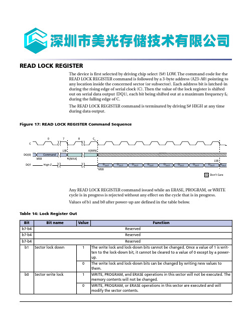
READ LOCK REGISTERThe device is first selected by driving chip select (S#) LOW. The command code for theREAD LOCK REGISTER command is followed by a 3-byte address (A23-A0) pointing toany location inside the concerned sector (or subsector). Each address bit is latched-induring the rising edge of serial clock (C). Then the value of the lock register is shiftedout on serial data output (DQ1), each bit being shifted out at a maximum frequency f C during the falling edge of C.The READ LOCK REGISTER command is terminated by driving S# HIGH at any timeduring data output.Figure 17: READ LOCK REGISTER Command SequenceDQ[0]CDQ1Don’t CareAny READ LOCK REGISTER command issued while an ERASE, PROGRAM, or WRITEcycle is in progress is rejected without any effect on the cycle that is in progress.Values of b1 and b0 after power-up are defined in the table below.Table 14: Lock Register OutPAGE ERASEThe PAGE ERASE command sets to 1 (FFh) all bits inside the chosen page. Before thePAGE ERASE command can be accepted, a WRITE ENABLE command must have beenexecuted previously. After the WRITE ENABLE command has been decoded, the devicesets the write enable latch (WEL) bit.The PAGE ERASE command is entered by driving chip select (S#) LOW, followed by thecommand code, and three address bytes on serial data input (DQ0). Any address insidethe sector is a valid address for the PAGE ERASE command. S# must be driven LOW forthe entire duration of the sequence.S# must be driven HIGH after the eighth bit of the last address byte has been latched in.Otherwise the PAGE ERASE command is not executed. As soon as S# is driven HIGH,the self-timed PAGE ERASE cycle is initiated; the cycle's duration is t PE. While the PAGEERASE cycle is in progress, the status register may be read to check the value of the writein progress (WIP) bit. The WIP bit is 1 during the self-timed PAGE ERASE cycle, and is 0when the cycle is completed. At some unspecified time before the cycle is completed,the WEL bit is reset.A PAGE ERASE command applied to a page that is hardware or software protected is notexecuted.A PAGE ERASE command while an ERASE, PROGRAM, or WRITE cycle is in progress isrejected without having any effects on the cycle that is in progress.If RESET# is driven LOW while a PAGE ERASE cycle is in progress, the PAGE ERASE cycleis interrupted and the programmed data may be corrupted. On RESET going LOW, thedevice enters the reset mode and a time of t RHSL is then required before the device canbe reselected by driving Chip Select (S#) LOW.Figure 21: PAGE ERASE Command SequenceCDQ0Notes: 1.Address bits A23-A18 are don't care in the M25PE20. Address bits A23-A17 are don'tcare in the M25PE10.2.Address bits A23-A19 are don't care.3.Address bits A23-A20 are don't care.SUBSECTOR ERASEThe SUBSECTOR ERASE command sets to 1 (FFh) all bits inside the chosen subsector.Before the SUBSECTOR ERASE command can be accepted, a WRITE ENABLE com-mand must have been executed previously. After the WRITE ENABLE command has been decoded, the device sets the write enable latch (WEL) bit.The SUBSECTOR ERASE command is entered by driving chip select (S#) LOW, followed by the command code, and three address bytes on serial data input (DQ0). Any address inside the subsector is a valid address for the SUBSECTOR ERASE command. S# must be driven LOW for the entire duration of the sequence.S# must be driven HIGH after the eighth bit of the last address byte has been latched in.Otherwise the SUBSECTOR ERASE command is not executed. As soon as S# is driven HIGH, the self-timed SUBSECTOR ERASE cycle is initiated; the cycle's duration is t SSE .While the SUBSECTOR ERASE cycle is in progress, the status register may be read to check the value of the write in progress (WIP) bit. The WIP bit is 1 during the self-timed SUBSECTOR ERASE cycle, and is 0 when the cycle is completed. At some unspecified time before the cycle is complete, the WEL bit is reset.A SUBSECTOR ERASE command issued to a sector that is hardware or software protec-ted is not executed.Any SUBSECTOR ERASE command issued while an ERASE, PROGRAM, or WRITE cycle is in progress is rejected without any effect on the cycle that is in progress.If RESET# is driven LOW while a SUBSECTOR ERASE cycle is in progress, the SUBSEC-TOR ERASE cycle is interrupted and data may not be erased correctly. On RESET# going LOW, the device enters the RESET mode and a time of t RHSL is then required before the device can be reselected by driving S# LOW.Figure 22: SUBSECTOR ERASE Command SequenceDQ0CS#2134567892930310Notes: 1.Address bits A23-A18 are don't care in the M25PE20. Address bits A23-A17 are don'tcare in the M25PE10.2.Address bits A23-A19 are don't care .3.Address bits A23-A20 are don't care .SECTOR ERASEThe SECTOR ERASE command sets to 1 (FFh) all bits inside the chosen sector. Before the SECTOR ERASE command can be accepted, a WRITE ENABLE command must have been executed previously. After the WRITE ENABLE command has been decoded, the device sets the write enable latch (WEL) bit.The SECTOR ERASE command is entered by driving chip select (S#) LOW, followed by the command code, and three address bytes on serial data input (DQ0). Any address in-side the sector is a valid address for the SECTOR ERASE command. S# must be driven LOW for the entire duration of the sequence.S# must be driven HIGH after the eighth bit of the last address byte has been latched in.Otherwise the SECTOR ERASE command is not executed. As soon as S# is driven HIGH,the self-timed SECTOR ERASE cycle is initiated; the cycle's duration is t SE . While the SECTOR ERASE cycle is in progress, the status register may be read to check the value of the write in progress (WIP) bit. The WIP bit is 1 during the self-timed SECTOR ERASE cycle, and is 0 when the cycle is completed. At some unspecified time before the cycle is completed, the WEL bit is reset.A SECTOR ERASE command applied to a sector that contains a page that is hardware protected is not executed.Any SECTOR ERASE command while an ERASE, PROGRAM, or WRITE cycle is in pro-gress is rejected without having any effects on the cycle that is in progress.If RESET# is driven LOW while a SECTOR ERASE cycle is in progress, the SECTORERASE cycle is interrupted and the programmed data may be corrupted. On RESET go-ing LOW, the device enters the reset mode and a time of t RHSL is then required before the device can be reselected by driving Chip Select (S#) LOW.Figure 23: SECTOR ERASE Command SequenceCDQ0S#2134567892930310Notes: 1.Address bits A23-A18 are don't care in the M25PE20. Address bits A23-A17 are don'tcare in the M25PE10.2.Address bits A23-A19 are don't care .3.Address bits A23-A20 are don't care .。
Gazelle S2028i(A) 模块化网管型二层工业以太网交换机 文档指南(Rel_03)
文档指南
对产品文档体系进行概要描述。 介绍了产品文档的组成、使用方 法、获取和反馈方式。
读者角色
网络规划工程师 硬件安装工程师 安装调测工程师 现场维护工程师 网络监控工程师 系统维护工程师 数据配置工程师
2-2
瑞斯康达科技发展股份有限公司
瑞斯康达 Gazelle S2028i(A)文档指南
2 产品文档使用方法
网络规划工程师硬件安装工程师安装调测工程师现场维护工程师网络监控工程师系统维护工程师数据配置工程师gazelles2028ia文档指南产品文档使用方法瑞斯康达科技发展股份有限公司23文档名称文档内容读者角色产品描述从产品整体角度出发进行简单且清晰地介绍包括
Gazelle S2028i(A) 模块化网管型二层工业以 太网交换机 文档指南 (Rel_03)
图1-1 Gazelle S2028i 产品文档组成
瑞斯康达科技发展股份有限公司
1-1
瑞斯康达 Gazelle S2028i(A)文档指南
2 产品文档使用方法
2 产品文档使用方法
2.1 分阶段使用文档
本节列举了不同阶段、不同任务内容所需要参考的主要文档和辅助文档。用户通过阅 读本章可以根据需求,找出所需要的文档,为设备的使用提供帮助。产品使用阶段对 应的文档请参见表 2-1。
配置指南(CLI) 配置指南(Web) 命令参考
瑞斯康达科技发展股份有限公司
2-1
2 产品文档使用方法
瑞斯康达 Gazelle S2028i(A)文档指南
2.2 分角色使用文档
2.2.1 角色划分说明
这里的角色划分可能会与读者实际角色有所不同,读者可根据提供的角色定义进行对 应。角色划分说明请参见表 2-2。
华为随行WiFi 2 系列参数表(包含包装盒尺寸 包装清单)
内置LTE/UMTS天线; 内置WLAN天线
SSID 广播和隐藏; None( Open)、 WPA2-PSK、 WPA/WPA2-PSK 加密方式; 速率自动调整; STA 状态显示; Wi-Fi 自动关闭; MAC 地址过滤 主机x1(产品内充电电池不可拆卸) USB线x1 挂绳 x1 (集成充电线) 快速入门x1 保修卡x1 电源适配器x1 TYPE C转接头x1
产品名称 产品尺寸(长×宽×高) 包装盒尺寸(长×宽×高) 产品重量 产品整机重量(含包装) 运营商网络制式 工作频段 Wi-Fi 标准 无线
接口类型
显示屏 电池容量
易用性 天线 加密方式
包装清单
华为随行 WiFi 2 Pro 112.0mm×69.2mm×23mm 156mm x 111mm x 69mm 约195g(含电池) 约533g 中国移动4G / 中国电信4G /中国联通4G /中国联通3G LTE FDD:B1/B2/B3/B4/B5/B7/B8/B20/B19 LTE TDD:B38/B40/B41(2555-2655MHz) UMTS:B1/B2/B4/B5/B6/B8/B19 GSM:B2/B3/B8/B5
802.11 ac/n/b/g标准,支持2.4G和5G品充电接口) 1个标准USB接口(对外充电接口) 1个标准micro SD卡槽 1个micro-SIM卡接口 1个自适应网口:RJ45
OLED-LCD 6400mAh(典型值)充电宝,支持对外充电,挂绳集成充电线(Micro USB接口) 工作时长25小时,待机时长1600小时
TL-R4238_R4239_R4299G用户手册
本手册所提到的产品规格和资讯仅供参考,如有内容更新,恕不另行通知。除非有特殊约定,本手 册仅作为使用指导,本手册中的所有陈述、信息等均不构成任何形式的担保。
目录
物 品 清 单 ........................................................................................................1 第 1 章 用户手册简介 ..................................................................................................................2
3.1.1 前面板................................................................................................................5 3.1.2 后面板................................................................................................................6 3.2 系统需求 .........................................................................................................................7 3.3 安装环境 .........................................................................................................................7 3.4 硬件安装步骤 ..................................................................................................................7 第 4 章 快速安装指南 ..................................................................................................................9 4.1 建立正确的网络设置........................................................................................................9 4.2 快速安装指南 ................................................................................................................10 第 5 章 配置指南 .......................................................................................................................13 5.1 启动和登录....................................................................................................................13 5.2 运行状态 .......................................................................................................................14 5.3 设置向导 .......................................................................................................................15 5.4 网络参数 .......................................................................................................................15 5.4.1 LAN口设置.......................................................................................................15 5.4.2 WAN口设置 .....................................................................................................16
WiLink 8 Pmod 适配器说明书
WiLink™ 8 Pmod Adaptor(Wi-Fi & Bluetooth interface board) Hardware User GuideVersion 1.0Page 1Document ControlDocument Version: 1.0Document Date:12/15/2014Version Date Comment1.0 12/15/2014 Initial ReleasePage 2Contents1Introduction (4)1.1Features (4)1.2Interfaces (4)1.3Pmod-PS (SDIO based WLAN Interface) (6)1.4Pmod-PL (UART based BT/BLE Interface) (6)1.5COM8 100 pin Wireless Module Connector (7)1.6Power (8)1.6.1 Power Input (8)1.6.2 Voltage Regulator (8)1.6.3 Bypassing/Decoupling (8)2Mechanical (9)2.1Dimensions (9)2.2Weight (9)Page 31 IntroductionThe TI WiLink™ 8 Pmod Adaptor is used to interface WiLink™ 8 Wi-Fi and Bluetooth/BLE evaluation boards from Texas Instruments via a Pmod compatible interface to “Zed-series” Avnet boards (MicroZed, Zedboard, PicoZed).At this time, the following two boards from TI are supported:WL1835MODCOM8B (2.4 GHz) andWL1837MODCOM8I (2.4 GHz/5.0 GHz, Industrial temperature grade)The WiLink™ 8 boar d provides the necessary voltage level translations to and from Pmod compatible interfaces.1.1 FeaturesThe WiLink™8 Adaptor facilitates the use of TI’s WL1835MODCOM8B Wi-Fi and BT/BLE module.Features of this wireless solution include the following:–WLAN, Bluetooth, BLE on a module board–WLAN 2.4 GHz SISO (20- and 40-MHz channels), 2.4-GHz MIMO (20-MHz channels)–Support for BLE dual mode–Seamless integration with Xilinx Zynq, TI Sitara and other application processors–Can be used with Avnet Zynq based boards or TI AM335X general-purpose EVM–WLAN and Bluetooth, BLE cores are software and hardware compatible with prior WL127x, WL128x and CC256x offerings, facilitating an easy migration to device.–Shared HCI transport for Bluetooth and BLE over UART and SDIO for WLAN.–Wi-Fi / Bluetooth single antenna co-existence–Built-in chip antenna as well as U.FL RF connectors for optional external 2.4-GHz band antenna–Bidirectional 3.3V & 1.8V voltage level translation on each Pmod connector.–VCCPmod power input – 3.3VDC on each Pmod connector–On board 1.8V Linear LDO regulator ensures reliable VIO voltage, current and noise margins.1.2 Interfaces–Two Pmod male headers connections J1 and J3.–J2 surface mount WL1835 COM module interface connector.Page 4Figure 1 –TI WiLink™ 8 Block DiagramFigure 2 –TI WiLink™ 8 Module with TI WL module attachedPage 51.3 Pmod-PS (SDIO based WLAN Interface)–SDIO 4-lane interface routed via Zynq MIO pins– 3.3V logic levels, signal names at the Pmod connectors as shown below are suffixed with an “_X” (as they connect to Xilinx device)Table 1 – Pmod-PS Interface Connections1.4 Pmod-PL (UART based BT/BLE Interface)–UART interface routed via Zynq EMIO pins– 3.3V logic levels, signal names are suffixed with “_X” (as they connect to Xilinx device)Table 2 – Pmod-PS Interface ConnectionsPage 61.5 COM8 100 pin Wireless Module Connector–Edge-Connector with 2x50 contacts (2-100 on component side, 1-99 on underside)–Only a subset of these signals are required to be routed on the Adaptor for full functionality.Table 3 – Pmod-PS Interface ConnectionsPage 71.6 Power1.6.1 Power InputThe board is powered via the Pmod J1 and Pmod J3 connector. Both 3.3V rails are joined onone VCCPmod plane.1.6.2 Voltage RegulatorThe 1.8V precision LDO regulator is a TI TPS73618DBVR SOT23-5 IC. This part features avery low drop out voltage (200mV max at full current) and a high current source capability(400mA) for its form factor. The device also features a 1% output precision under all line, loadand thermal conditions. For further device information please see the TI datasheet.The table below shows the minimum required voltage rails, currents, and tolerances.Table 3 – Voltage Rails w/ Current Estimates1.6.3 Bypassing/DecouplingThe TI WiLink™ 8 follows the recommended decoupling techniques pereach manufacturer’s datasheet.Page 82 Mechanical2.1 DimensionsFigure 5: TI WiLink-8 Dimensions (mils)2.2 WeightThe weight of the WiLink™ 8 adaptor is 8 grams (~0.25 ounces) standalone and15 grams (~0.5 oz) with a TI Wi-Fi module inserted.Page 9。
- 1、下载文档前请自行甄别文档内容的完整性,平台不提供额外的编辑、内容补充、找答案等附加服务。
- 2、"仅部分预览"的文档,不可在线预览部分如存在完整性等问题,可反馈申请退款(可完整预览的文档不适用该条件!)。
- 3、如文档侵犯您的权益,请联系客服反馈,我们会尽快为您处理(人工客服工作时间:9:00-18:30)。
深圳信诺山通信技术有限公司Shenzhen Signalsen Telecom Technology Co,.Ltd
规格书
喜瑞得(2928)
料号:W19-1Y90A-F
1. 项目图片
项目图片如下:
2.测试制具
目的:尽可能准确地测试天线的无源参数。
制作方法:手机制具是用一根50欧姆的同轴电缆,一端连在手机主板的匹配电路后端(射频测试孔前端)的测试点上,另一端连接SMA接头。
示意图如下:
3. 匹配电路
原匹配无更改。
4. S11测试
4.0 S11测试方法说明
测试设备:网络分析仪(HP 8753E)
测试方法:用一根50欧姆CABLE电缆从仪器测试端口导出,使用校准件校准后连接射频治具的SMA接头,记录相关频点对应的回波损耗和驻波比。
测试示意图如下:
测试示意图4.1S11参数
驻波:
8. 结构图纸。