2N系列功率晶体管技术参数(精)
2N3500、2N3501NPN晶体管产品规格书
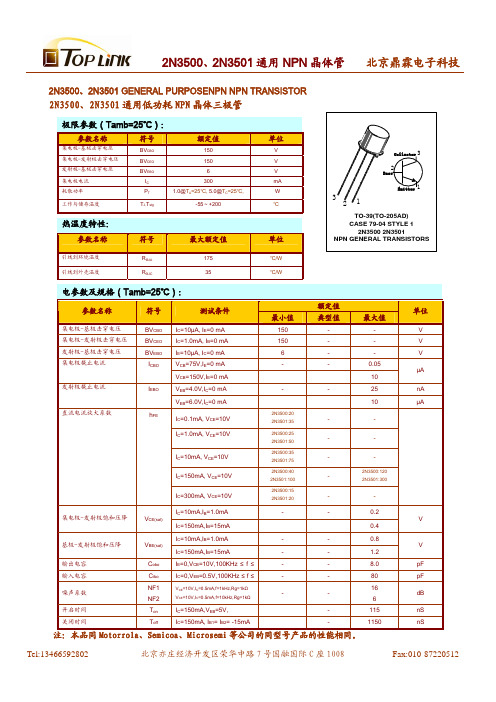
2N3500、2N3501 GENERAL PURPOSENPN NPN TRANSISTOR
2N3500、2N3501 通用低功耗 NPN 晶体三极管
极限参数(Tamb=25℃):
参数名称
集电极-基极击穿电压 集电极-发射极击穿电压 发射极-基极击穿电压 集电极电流 耗散功率
-
NF2
VCE=10V,IC=0.5mA,f=10kHz,Rg=1kΩ
16 -
6
开启时间
Ton
IC=150mA,VEB=5V,
-
115
关闭时间
Toff
IC=150mA, IB1= IB2= -15mA
-
1150
注:本品同 Motorrola、Semicoa、Microsemi 等公司的同型号产品的性能相同。
2N3500:35
2N3501:75
-
-
2N3500:40
2N3500:120
2N3501:100
-
2N3501:300
2N3500:15
2N3501:20
-
-
集电极-发射极饱和压降
VCE(sat)
IC=10mA,IB=1.0mA IC=150mA,IB=15mA
-
-
0.2
0.4
基极-发射极饱和压降
VBE(sat)
IC=10mA,IB=1.0mA IC=150mA,IB=15mA
-
-
0.8
-
-
1.2
输出电容
Cobo
IE=0,VCB=10V,100KHz ≤ f ≤
-
-
2n3866参数

2n3866参数(实用版)目录1.2n3866 概述2.2n3866 的主要参数3.2n3866 参数的详细说明正文2n3866 是一款常见的电子元器件,广泛应用于各种电子设备中。
了解 2n3866 的参数对于选择和使用该元器件至关重要。
下面我们将详细介绍 2n3866 的主要参数及其含义。
首先,我们来了解一下 2n3866 的基本概述。
2n3866 是一种双极型晶体管,具有放大和开关等功能。
它主要由三个区域组成:n 型区、p 型区和 n 型区,其中两个 n 型区之间夹着一个 p 型区。
这种结构使得2n3866 具有很高的电流放大能力和良好的开关特性。
接下来,我们来看一下 2n3866 的主要参数。
在查阅相关资料时,我们通常会看到以下几个参数:1.集电极电流(IC):集电极电流是晶体管工作时流经集电极的电流。
它是晶体管的一个重要参数,决定了晶体管的电流放大能力。
2.集电极 - 发射极电压(VCE):集电极 - 发射极电压是指在晶体管工作时,集电极和发射极之间的电压。
这个参数影响了晶体管的输出特性。
3.发射极电流(IE):发射极电流是指在晶体管工作时流经发射极的电流。
发射极电流与集电极电流之间有一定的关系,通常用来评价晶体管的电流放大能力。
4.功耗(PD):功耗是指晶体管在工作过程中消耗的功率。
功耗与晶体管的电流和电压有关,对晶体管的可靠性和稳定性有重要影响。
在了解了 2n3866 的主要参数后,我们还需要对这些参数进行详细说明,以便更好地理解和应用这款元器件。
以下是 2n3866 参数的详细说明:1.集电极电流(IC):集电极电流是 2n3866 最重要的参数之一。
根据不同的使用场景,我们可以选择具有不同集电极电流的 2n3866。
通常情况下,集电极电流越大,晶体管的电流放大能力越强。
2.集电极 - 发射极电压(VCE):集电极 - 发射极电压决定了晶体管的开关速度。
在实际应用中,我们需要根据电路的要求选择合适的 VCE 值。
2n5401的管脚和参数
2n5401的管脚和参数
2N5401是一种PNP极性的晶体管,它有三个引脚,发射极(E),基极(B)和集电极(C)。
在引脚排列上,通常来说,从正
面看,引脚从左到右的排列顺序是,发射极、基极、集电极。
至于参数,2N5401的典型参数包括最大集电极-发射极电压(VCEO)为150V,最大集电极-基极电压(VCBO)为160V,最大发
射极-基极电压(VEBO)为5V。
最大集电极电流(IC)为600mA,最
大功率(Ptot)为625mW。
此外,它的直流增益(hFE)在100到
250之间。
这些参数对于设计电路和选择适当的工作条件非常重要。
除了这些基本参数之外,还有一些其他的参数,比如最大封装
温度(Tj),最大存储温度(Tstg)等等,这些参数对于在特定环
境条件下的应用也非常重要。
总的来说,了解2N5401的管脚和参数对于工程师在电路设计和
应用中起着至关重要的作用,因为它们直接影响着晶体管的工作性
能和可靠性。
希望这些信息能够帮助你更好地了解2N5401晶体管。
2n5416参数
2n5416参数
2n5416是一款双极型PNP晶体管,通常用于低功耗放大器、开关和线性稳压器等电路中。
它具有高电压容忍度和低噪声特性,适合用于需要高性能的电子设备。
在电子领域中,晶体管是一种重要的电子元件,广泛应用于各种电路中。
2n5416作为一款高性能的PNP晶体管,具有许多优点。
首先,它的封装结构紧凑,体积小巧,适合于空间有限的电路设计。
其次,2n5416具有较高的电压容忍度,能够承受较高的电压,保证电路的稳定性和可靠性。
此外,它还具有低噪声特性,适合用于对信号质量要求较高的电路中。
在低功耗放大器中,2n5416可以发挥其优良的放大特性。
通过合理设计电路,可以实现信号的放大和处理,保证信号的清晰度和稳定性。
在开关电路中,2n5416可以作为开关管使用,控制电路的通断,实现电路的开关功能。
此外,在线性稳压器中,2n5416可以帮助实现电压的稳定输出,保证电路的正常工作。
除了在以上应用中,2n5416还可以用于其他各种电子设备中,如功率放大器、振荡器、脉冲电路等。
由于其高性能和稳定性,2n5416受到广泛关注和应用。
总的来说,2n5416作为一款高性能的双极型PNP晶体管,在各种电子设备中都有着重要的应用。
其小巧的封装、高电压容忍度和低
噪声特性,使其成为电路设计中的重要组成部分。
通过合理选择和设计电路,可以充分发挥2n5416的优良特性,确保电子设备的性能和稳定性。
希望未来能够有更多的电子元件能够像2n5416一样,为电子技术的发展做出贡献。
2n3771 2n3772 高功率npn 硅功率晶体管 数据表.pdf说明书
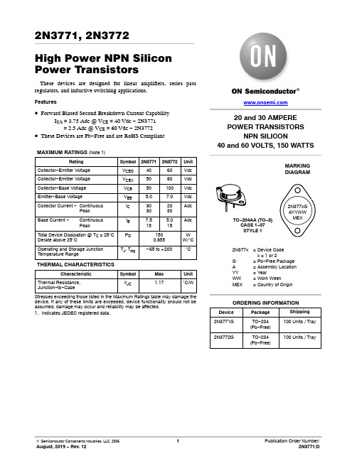
2N3771, 2N3772High Power NPN Silicon Power TransistorsThese devices are designed for linear amplifiers, series pass regulators, and inductive switching applications.Features•Forward Biased Second Breakdown Current CapabilityI S/b= 3.75 Adc @ V CE = 40 Vdc − 2N3771= 2.5 Adc @ V CE = 60 Vdc − 2N3772•These Devices are Pb−Free and are RoHS Compliant MAXIMUM RATINGS (Note 1)Rating Symbol2N37712N3772Unit Collector−Emitter Voltage V CEO4060Vdc Collector−Emitter Voltage V CEX5080Vdc Collector−Base Voltage V CB50100Vdc Emitter−Base Voltage V EB 5.07.0VdcCollector Current −ContinuousPeak I C30302030AdcBase Current −ContinuousPeak I B7.5155.015AdcT otal Device Dissipation @ T C = 25°C Derate above 25°C P D1500.855WW/°COperating and Storage JunctionTemperature RangeT J, T stg–65 to +200°C THERMAL CHARACTERISTICSCharacteristic Symbol Max Unit Thermal Resistance,Junction−to−Caseq JC 1.17°C/WStresses exceeding those listed in the Maximum Ratings table may damage the device. If any of these limits are exceeded, device functionality should not be assumed, damage may occur and reliability may be affected.1.Indicates JEDEC registered data.20 and 30 AMPEREPOWER TRANSISTORSNPN SILICON40 and 60 VOLTS, 150 WATTSMARKINGDIAGRAMTO−204AA (TO−3)CASE 1−07STYLE 12N377x=Device Codex = 1 or 2G=Pb−Free PackageA=Assembly LocationYY=YearWW=Work WeekMEX=Country of Origin2N377xGAYYWWMEX2N3772G TO−204(Pb−Free)100 Units / Tray Device Package Shipping2N3771G TO−204(Pb−Free)100 Units / Tray ORDERING INFORMATIONELECTRICAL CHARACTERISTICS (T C= 25_C unless otherwise noted)Characteristic Symbol Min Max Unit OFF CHARACTERISTICSCollector−Emitter Sustaining Voltage (Note 2 and 3)2N3771(I C = 0.2 Adc, I B = 0)2N3772V CEO(sus)4060−−VdcCollector−Emitter Sustaining Voltage2N3771(I C = 0.2 Adc, V EB(off) = 1.5 Vdc, R BE = 100 W)2N3772V CEX(sus)5080−−VdcCollector−Emitter Sustaining Voltage2N3771(I C = 0.2 Adc, R BE = 100 W)2N3772V CER(sus)4570−−VdcCollector Cutoff Current (Note 2)(V CE = 30 Vdc, I B = 0)2N3771 (V CE = 50 Vdc, I B = 0)2N3772 (V CE = 25 Vdc, I B = 0)I CEO−−1010mAdcCollector Cutoff Current (Note 2)(V CE = 50 Vdc, V EB(off) = 1.5 Vdc)2N3771 (V CE = 100 Vdc, V EB(off) = 1.5 Vdc)2N3772 (V CE = 45 Vdc, V EB(off) = 1.5 Vdc)2N6257 (V CE = 30 Vdc, V EB(off) = 1.5 Vdc, T C = 150_C)2N37712N3772 (V CE = 45 Vdc, V EB(off) = 1.5 Vdc, T C = 150_C)I CEV−−−−−2.05.04.01010mAdcCollector Cutoff Current (Note 2)(V CB = 50 Vdc, I E = 0)2N3771 (V CB = 100 Vdc, I E = 0)2N3772I CBO−−2.05.0mAdcEmitter Cutoff Current (Note 2)(V BE = 5.0 Vdc, I C = 0)2N3771 (V BE = 7.0 Vdc, I C = 0)2N3772I EBO−−5.05.0mAdcON CHARACTERISTICS (Note 2)DC Current Gain (Note 3)(I C = 15 Adc, V CE = 4.0 Vdc)2N3771(I C = 10 Adc, V CE = 4.0 Vdc)2N3772(I C = 8.0 Adc, V CE = 4.0 Vdc)(I C = 30 Adc, V CE = 4.0 Vdc)2N3771(I C = 20 Adc, V CE = 4.0 Vdc)2N3772h FE15155.05.06060−−−Collector−Emitter Saturation Voltage(I C = 15 Adc, I B = 1.5 Adc)2N3771(I C = 10 Adc, I B = 1.0 Adc)2N3772(I C = 30 Adc, I B = 6.0 Adc)2N3771(I C = 20 Adc, I B = 4.0 Adc)2N3772V CE(sat)−−−−2.01.44.04.0VdcBase−Emitter On Voltage(I C = 15 Adc, V CE = 4.0 Vdc)2N3771(I C = 10 Adc, V CE = 4.0 Vdc)2N3772(I C = 8.0 Adc, V CE = 4.0 Vdc)V BE(on)−−2.72.2Vdc*DYNAMIC CHARACTERISTICS (Note 2)Current−Gain — Bandwidth Product(I C = 1.0 Adc, V CE = 4.0 Vdc, f test = 50 kHz)f T0.2−MHzSmall−Signal Current Gain(I C = 1.0 Adc, V CE = 4.0 Vdc, f = 1.0 kHz)h fe40−−SECOND BREAKDOWNSecond Breakdown Energy with Base Forward Biased, t = 1.0 s (non−repetitive) (V CE = 40 Vdc)2N3771 (V CE = 60 Vdc)2N3772I S/b3.752.5−−Adc2.Indicates JEDEC registered data.3.Pulse Test: 300 m s, Rep. Rate 60 cps.20000255075100125150175200Figure 1. Power DeratingT C , CASE TEMPERATURE (°C)1501005025P D , P O W E R D I S S I P A T I O N (W A T T S )17512575Figure 2. Thermal Response — 2N3771, 2N3772t, TIME (ms)r (t ), E F F E C T I V E T R A N S I E N T T H E R M A L R E S I S T A N C E (N O R M A L I Z E D )40Figure 3. Active −Region Safe Operating Area— 2N3771, 2N3772V CE , COLLECTOR-EMITTER VOLTAGE (VOLTS)3020102.07.0I C , C O L L E C T O R C U R R E N T (A M P )5.03.0There are two limitations on the power handling ability of a transistor: average junction temperature and second breakdown. Safe operating area curves indicate I C − V CE limits of the transistor that must be observed for reliable operation: i.e., the transistor must not be subjected to greater dissipation than the curves indicate.Figure 3 is based on JEDEC registered Data. Second breakdown pulse limits are valid for duty cycles to 10%provided T J(pk) < 200_C. T J(pk) may be calculated from the data of Figure 2. Using data of Figure 2 and the pulse power limits of Figure 3, T J(pk) will be found to be less than T J(max)for pulse widths of 1 ms and less. When using ON Semiconductor transistors, it is permissible to increase the pulse power limits until limited by T J(max).Figure 4. Switching Time Test CircuitSCOPEV CC t r , t f ≤ 10 ns DUTY CYCLE = 1.0%D1 MUST BE FAST RECOVERY TYPE, e.g.: 1N5825 USED ABOVE I B ≈ 100 mA MSD6100 USED BELOW I B ≈ 100 mAR B AND R C ARE VARIED TO OBTAIN DESIRED CURRENT LEVELS10Figure 5. Turn −On TimeI C , COLLECTOR CURRENT (AMP)5.02.01.00.50.20.10.010.05t , T I M E ( s )μ0.02V C E , C O L L E C T O R -E M I T T E R V O L T A G E (V O L T S )Figure 6. Turn −Off TimeI C , COLLECTOR CURRENT (AMP)t , T I M E ( s )μ2000Figure 7. CapacitanceV R , REVERSE VOLTAGE (VOLTS)200C , C A P A C I T A N C E (p F )1000700500300500Figure 8. DC Current GainI C , COLLECTOR CURRENT (AMP)5.010********h F E , D C C U R R E N T G A I N3007030107.0Figure 9. Collector Saturation RegionI B , BASE CURRENT (AMP)MECHANICAL CASE OUTLINEPACKAGE DIMENSIONSSCALE 1:1CASE 1−07ISSUE Z DATE 05/18/1988 TO−204 (TO−3)NOTES:1.DIMENSIONING AND TOLERANCING PER ANSIY14.5M, 1982.2.CONTROLLING DIMENSION: INCH.3.ALL RULES AND NOTES ASSOCIATED WITHREFERENCED TO-204AA OUTLINE SHALL APPLY.STYLE 1:PIN 1.BASE2.EMITTER CASE:COLLECTOR STYLE 2:PIN 1.BASE2.COLLECTORCASE:EMITTERSTYLE 3:PIN 1.GATE2.SOURCECASE:DRAINSTYLE 4:PIN 1.GROUND2.INPUTCASE:OUTPUTSTYLE 5:PIN 1.CATHODE2.EXTERNAL TRIP/DELAYCASE:ANODESTYLE 6:PIN 1.GATE2.EMITTER CASE:COLLECTOR STYLE 7:PIN 1.ANODE2.OPENCASE:CATHODESTYLE 8:PIN 1.CATHODE #12.CATHODE #2CASE:ANODESTYLE 9:PIN 1.ANODE #12.ANODE #2CASE:CATHODEDIM MIN MAX MIN MAXMILLIMETERSINCHESA 1.550 REF39.37 REFB--- 1.050---26.67C0.2500.335 6.358.51D0.0380.0430.97 1.09E0.0550.070 1.40 1.77G0.430 BSC10.92 BSCH0.215 BSC 5.46 BSCK0.4400.48011.1812.19L0.665 BSC16.89 BSCN---0.830---21.08Q0.1510.165 3.84 4.19U 1.187 BSC30.15 BSCV0.1310.188 3.33 4.77ON Semiconductor and are trademarks of Semiconductor Components Industries, LLC (SCILLC). SCILLC reserves the right to make changes without further notice to any products herein. SCILLC makes no warranty, representation or guarantee regarding the suitability of its products for any particular purpose, nor does SCILLC assume any liability arising out of the application or use of any product or circuit, and specifically disclaims any and all liability, including without limitation special, consequential or incidental damages. “Typical” parameters which may be provided in SCILLC data sheets and/or specifications can and do vary in different applications and actual performance may vary over time. All operating parameters, including “Typicals” must be validated for each customer application by customer’s technical experts. SCILLC does not convey any license under its patent rights nor the rights of others. SCILLC products are not designed, intended, or authorized for use as components in systems intended for surgical implant into the body, or other applications intended to support or sustain life, or for any other application in which the failure of the SCILLC product could create a situation where personal injury or death may occur. Should Buyer purchase or use SCILLC products for any such unintended or unauthorized application, Buyer shall indemnify and hold SCILLC and its officers, employees, subsidiaries, affiliates, and distributors harmless against all claims, costs, damages, and expenses, and reasonable attorney fees arising out of, directly or indirectly, any claim of personal injury or death associated with such unintended or unauthorized use, even if such claim alleges that SCILLC was negligent regarding the design or manufacture of the part. SCILLC is an Equal Opportunity/Affirmative Action Employer.PUBLICATION ORDERING INFORMATIONTECHNICAL SUPPORTNorth American Technical Support:Voice Mail: 1 800−282−9855 Toll Free USA/Canada Phone: 011 421 33 790 2910LITERATURE FULFILLMENT :Email Requests to:*******************onsemi Website: Europe, Middle East and Africa Technical Support:Phone: 00421 33 790 2910For additional information, please contact your local Sales Representative。
2n5302高功率npn硅晶体管说明书

2N5302High−Power NPN Silicon TransistorHigh−power NPN silicon transistors are for use in power amplifier and switching circuits applications.Features•Low Collector−Emitter Saturation V oltage −V CE(sat) = 0.75 Vdc (Max) @ I C = 10 Adc •Pb−Free Package is Available*MAXIMUM RATINGS (Note 1) (T J = 25°C unless otherwise noted)RatingSymbol Value Unit Collector−Emitter Voltage V CEO 60Vdc Collector−Base VoltageV CB 60Vdc Collector Current − Continuous (Note 2)I C 30Adc Base CurrentI B7.5AdcTotal Device Dissipation @ T C = 25_C Derate above 25_CP D 2001.14WW/_C Operating and Storage Junction Temperature RangeT J , T stg–65 to +200_CTHERMAL CHARACTERISTICSCharacteristicSymbol Max Unit Thermal Resistance, Junction−to−Case q JC 0.875_C/W Thermal Resistance, Case−to−Ambientq CA34_C/WStresses exceeding Maximum Ratings may damage the device. MaximumRatings are stress ratings only. Functional operation above the Recommended Operating Conditions is not implied. Extended exposure to stresses above the Recommended Operating Conditions may affect device reliability.1.Indicates JEDEC Registered Data.2.Pulse Test: Pulse Width = 5 m s, Duty Cycle ≤ 10%.2000Figure 1. Power Temperature Derating CurveTEMPERATURE (°C)P D , P O W E R D I S S I P A T I O N (W A T T S )15010050T C 8.006.04.02.0T A *For additional information on our Pb−Free strategy and soldering details, please download the ON Semiconductor Soldering and Mounting Techniques Reference Manual, SOLDERRM/D.Device Package Shipping ORDERING INFORMATION2N5302TO−204100 Units/Tray 2N5302GTO−204(Pb−Free)100 Units/TrayELECTRICAL CHARACTERISTICS (T C = 25_C unless otherwise noted)CharacteristicSymbol Min MaxUnitOFF CHARACTERISTICS (Note 3)Collector−Emitter Sustaining Voltage (Note 4)(I C = 200 mAdc, I B = 0)V CEO(sus)60−VdcCollector Cutoff Current (V CE = 60 Vdc, I B = 0)I CEO − 5.0mAdcCollector Cutoff Current(V CE = 60 Vdc, VEB(off) = 1.5 Vdc)I CEX − 1.0mAdc Collector Cutoff Current(V CE = 60 Vdc, V EB(off) = 1.5 Vdc, T C = 150_C)I CEX−10mAdcCollector Cutoff Current (V CB = 80 Vdc, I E = 0)I CBO − 1.0mAdcEmitter Cutoff Current (V BE = 5.0 Vdc, I C = 0)I EBO −5.0mAdc ON CHARACTERISTICSDC Current Gain (Note 4)*(I C = 1.0 Adc, V CE = 2.0 Vdc)*(I C = 15 Adc, V CE = 2.0 Vdc)(I C = 30 Adc, V CE = 4.0 Vdc)h FE40155.0−60−−*Collector−Emitter Saturation Voltage (Note 4)(I C = 10 Adc, I B = 1.0 Adc)(I C = 20 Adc, I B = 2.0 Adc)2(I C = 30 Adc, I B = 6.0 Adc)V CE(sat)−−−0.752.03.0Vdc*Base Emitter Saturation Voltage (Note 4)(I C = 10 Adc, I B = 1.0 Adc)(I C = 15 Adc, I B = 1.5 Adc)(I C = 20 Adc, I B = 2.0 Adc)V BE(sat)−−− 1.71.82.5Vdc*Base−Emitter On Voltage (Note 4)(I C = 15 Adc, V CE = 2.0 Vdc)(I C = 30 Adc, V CE = 4.0 Vdc)V BE(on)−−1.73.0VdcDYNAMIC CHARACTERISTICS (Note 3)Current−Gain − Bandwidth Product (I C = 1.0 Adc, V CE = 10 Vdc, f = 1.0 MHz)f T2.0−MHz Small−Signal Current Gain (I C = 1.0 Adc, V CE = 10 Vdc, f = 1.0 kHz)h fe40−−SWITCHING CHARACTERISTICS (Note 3)Rise Time (V CC = 30 Vdc, I C = 10 Adc, I B1 = I B2 = 1.0 Adc)t r− 1.0m s Storage Time t s − 2.0m s Fall Timet f−1.0m s3.Indicates JEDEC Registered Data.4.Pulse Width v 300 m s, Duty Cycle v 2.0%.SWITCHING TIME EQUIVALENT TEST CIRCUITSFigure 2. Turn−On time+11 V− 2V TO Figure 3. Turn−Off time+11 V− 9V TO 0BBr (t ), N O R M A L I Z E D E F F E C T I V E T R A N S I E N T T H E R M A L R E S I S T A N C E100Figure 5. Active−Region Safe Operating Area V CE , COLLECTOR−EMITTER VOLTAGE (VOLTS)5020105.02.01.00.50.10.2I C , C O L L E C T O R C U R R E N T (A M P )Figure 6. Capacitance versus VoltageV R , REVERSE VOLTAGE (VOLTS)5.0I C , COLLECTOR CURRENT (AMP)3.02.00.70.50.30.10.050.07t , T I M E ( s )μFigure 7. Turn−On Time 1.00.2I C , COLLECTOR CURRENT (AMP)Figure 8. Turn−Off Time)R B E , E X T E R N A L B A S E −E M I T T E R R E S I S T A N C E (O H M S )300Figure 9. DC Current GainI C , COLLECTOR CURRENT (AMP)10100503020Figure 10. Collector Saturation RegionI B , BASE CURRENT (AMP)20070h F E , D C C U R R E N T G A I N108Figure 11. Effects of Base−Emitter Resistance T J , JUNCTION TEMPERATURE (°C)1061051041031021072.0I C , COLLECTOR CURRENT (AMP)1.60.80.60.40V , V O L T A G E (V O L T S )Figure 12. “On” Voltages1.81.41.21.00.2103− Figure 13. Collector Cut−Off Region V BE , BASE−EMITTER VOLTAGE (VOLTS)10210110010−1, C O L L E C T O R C U R R E N T ( A )μI C 10− 10− Figure 14. Temperature CoefficientsI C , COLLECTOR CURRENT (AMP)MECHANICAL CASE OUTLINEPACKAGE DIMENSIONSSCALE 1:1CASE 1−07ISSUE Z DATE 05/18/1988 TO−204 (TO−3)NOTES:1.DIMENSIONING AND TOLERANCING PER ANSIY14.5M, 1982.2.CONTROLLING DIMENSION: INCH.3.ALL RULES AND NOTES ASSOCIATED WITHREFERENCED TO-204AA OUTLINE SHALL APPLY.STYLE 1:PIN 1.BASE2.EMITTER CASE:COLLECTOR STYLE 2:PIN 1.BASE2.COLLECTORCASE:EMITTERSTYLE 3:PIN 1.GATE2.SOURCECASE:DRAINSTYLE 4:PIN 1.GROUND2.INPUTCASE:OUTPUTSTYLE 5:PIN 1.CATHODE2.EXTERNAL TRIP/DELAYCASE:ANODESTYLE 6:PIN 1.GATE2.EMITTER CASE:COLLECTOR STYLE 7:PIN 1.ANODE2.OPENCASE:CATHODESTYLE 8:PIN 1.CATHODE #12.CATHODE #2CASE:ANODESTYLE 9:PIN 1.ANODE #12.ANODE #2CASE:CATHODEDIM MIN MAX MIN MAXMILLIMETERSINCHESA 1.550 REF39.37 REFB--- 1.050---26.67C0.2500.335 6.358.51D0.0380.0430.97 1.09E0.0550.070 1.40 1.77G0.430 BSC10.92 BSCH0.215 BSC 5.46 BSCK0.4400.48011.1812.19L0.665 BSC16.89 BSCN---0.830---21.08Q0.1510.165 3.84 4.19U 1.187 BSC30.15 BSCV0.1310.188 3.33 4.77ON Semiconductor and are trademarks of Semiconductor Components Industries, LLC (SCILLC). SCILLC reserves the right to make changes without further notice to any products herein. SCILLC makes no warranty, representation or guarantee regarding the suitability of its products for any particular purpose, nor does SCILLC assume any liability arising out of the application or use of any product or circuit, and specifically disclaims any and all liability, including without limitation special, consequential or incidental damages. “Typical” parameters which may be provided in SCILLC data sheets and/or specifications can and do vary in different applications and actual performance may vary over time. All operating parameters, including “Typicals” must be validated for each customer application by customer’s technical experts. SCILLC does not convey any license under its patent rights nor the rights of others. SCILLC products are not designed, intended, or authorized for use as components in systems intended for surgical implant into the body, or other applications intended to support or sustain life, or for any other application in which the failure of the SCILLC product could create a situation where personal injury or death may occur. Should Buyer purchase or use SCILLC products for any such unintended or unauthorized application, Buyer shall indemnify and hold SCILLC and its officers, employees, subsidiaries, affiliates, and distributors harmless against all claims, costs, damages, and expenses, and reasonable attorney fees arising out of, directly or indirectly, any claim of personal injury or death associated with such unintended or unauthorized use, even if such claim alleges that SCILLC was negligent regarding the design or manufacture of the part. SCILLC is an Equal Opportunity/Affirmative Action Employer.PUBLICATION ORDERING INFORMATIONTECHNICAL SUPPORTNorth American Technical Support:Voice Mail: 1 800−282−9855 Toll Free USA/Canada Phone: 011 421 33 790 2910LITERATURE FULFILLMENT :Email Requests to:*******************onsemi Website: Europe, Middle East and Africa Technical Support:Phone: 00421 33 790 2910For additional information, please contact your local Sales Representative。
三极管参数型号范文
三极管参数型号范文三极管是一种常用的半导体器件,用于放大电路、开关电路以及作为电子元器件。
它由三个PN结组成,分别称为基极、发射极和集电极。
三极管的性能与参数型号直接相关,包括最大电流、最大电压、最大功率、放大倍数等。
以下是一些常见的三极管参数型号的介绍。
1.2N2222(NPN型)2N2222是一种经典的NPN型晶体管,常用于低功率放大和开关应用。
它的最大电流为600mA,最大电压为30V,具有中等放大倍数。
2.BC548(NPN型)BC548是一种常用的NPN型小功率晶体管,适用于低噪声放大、振荡电路等应用。
它的最大电流为100mA,最大电压为30V,放大倍数较高。
3.BC556(PNP型)BC556是一种常用的PNP型小功率晶体管,适用于低噪声放大、振荡电路等应用。
它的最大电流为100mA,最大电压为65V,放大倍数较高。
4.2N3055(NPN型功放晶体管)2N3055是一种大功率NPN型晶体管,适用于功率放大和开关电路等高功率应用。
它的最大电流为15A,最大电压为60V,可以提供较高的功率放大倍数。
5.TIP41C(NPN型功放晶体管)TIP41C是一种常用的NPN型功放晶体管,适用于中等功率放大和开关电路等应用。
它的最大电流为6A,最大电压为40V,能够提供适度的功率放大倍数。
6.TIP31C(NPN型功放晶体管)TIP31C是一种常用的NPN型功放晶体管,适用于中等功率放大和开关电路等应用。
它的最大电流为3A,最大电压为40V,具有较高的功率放大倍数。
8.BD140(PNP型功放晶体管)BD140是一种PNP型功放晶体管,适用于低功率放大和开关电路等应用。
它的最大电流为1.5A,最大电压为80V,具有中等放大倍数。
除了上述介绍的几种常见的三极管参数型号,还有其他多种型号的三极管可供选择。
不同的型号有不同的特性和应用范围,可以根据具体的电路需求选择合适的型号。
2n6040 2n6042 2n6043 2n6045 塑料中功率互补硅晶体管 数据表 smd to
PNP - 2N6040, 2N6042,NPN - 2N6043, 2N6045 Plastic Medium-Power Complementary Silicon TransistorsPlastic medium−power complementary silicon transistors are designed for general−purpose amplifier and low−speed switching applications.Features•High DC Current Gain − h FE = 2500 (Typ) @ I C = 4.0 Adc •Collector−Emitter Sustaining V oltage − @ 100 mAdc −V CEO(sus) = 60 Vdc (Min) − 2N6040, 2N6043= 100 Vdc (Min) − 2N6042, 2N6045•Low Collector−Emitter Saturation V oltage −V CE(sat) = 2.0 Vdc (Max) @ I C = 4.0 Adc − 2N6043,44= 2.0 Vdc (Max) @ I C = 3.0 Adc − 2N6042, 2N6045•Monolithic Construction with Built−In Base−Emitter Shunt Resistors •EpoxyMeetsUL94V−*********•ESD Ratings:Human Body Model, 3B > 8000 VMachine Model, C > 400 V•These Devices are Pb−Free and are RoHS Compliant*MAXIMUM RATINGS (Note 1)Rating Symbol Value UnitCollector−Emitter Voltage2N60402N60432N60422N6045V CEO60100VdcCollector−Base Voltage2N60402N60432N60422N6045V CB60100VdcEmitter−Base Voltage V EB 5.0VdcCollector Current ContinuousPeak I C8.016AdcBase Current I B120mAdcTotal Power Dissipation @ T C = 25°C Derate above 25°C P D750.60WW/°COperating and Storage JunctionTemperature RangeT J, T stg–65 to +150°CStresses exceeding those listed in the Maximum Ratings table may damage the device. If any of these limits are exceeded, device functionality should not be assumed, damage may occur and reliability may be affected.1.Indicates JEDEC Registered Data.*For additional information on our Pb−Free strategy and soldering details, please download the ON Semiconductor Soldering and Mounting Techniques Reference Manual, SOLDERRM/D.TO−220CASE 221ASTYLE 1MARKING DIAGRAM2N604x=Device Codex = 0, 2, 3, or 5A= Assembly LocationY= YearWW= Work WeekG= Pb−Free PackageDARLINGTON, 8 AMPERES COMPLEMENTARY SILICON POWER TRANSISTORS60 − 100 VOLTS, 75 WATTSSee detailed ordering and shipping information in the package dimensions section on page 5 of this data sheet.ORDERING INFORMATIONTHERMAL CHARACTERISTICSCharacteristic Symbol Max Unit Thermal Resistance, Junction−to−Case q JC 1.67°C/W Thermal Resistance, Junction−to−Ambient q JA57°C/W*ELECTRICAL CHARACTERISTICS (T C = 25°C unless otherwise noted)Characteristic Symbol Min Max Unit OFF CHARACTERISTICSCollector−Emitter Sustaining Voltage(I C = 100 mAdc, I B = 0)2N6040, 2N60432N6042, 2N6045V CEO(sus)60100−−VdcCollector Cutoff Current(V CE = 60 Vdc, I B = 0)2N6040, 2N6043 (V CE = 100 Vdc, I B = 0)2N6042, 2N6045I CEO−−2020m ACollector Cutoff Current(V CE = 60 Vdc, V BE(off) = 1.5 Vdc)2N6040, 2N6043 (V CE = 100 Vdc, V BE(off) = 1.5 Vdc)2N6042, 2N6045 (V CE = 60 Vdc, V BE(off) = 1.5 Vdc, T C = 150°C)2N6040, 2N6043 (V CE = 80 Vdc, V BE(off) = 1.5 Vdc, T C = 150°C)2N6041, 2N6044 (V CE = 100 Vdc, V BE(off) = 1.5 Vdc, T C = 150°C)2N6042, 2N6045I CEX−−−−−2020200200200m ACollector Cutoff Current(V CB = 60 Vdc, I E = 0)2N6040, 2N6043 (V CB = 100 Vdc, I E = 0)2N6042, 2N6045I CBO−−2020m AEmitter Cutoff Current (V BE = 5.0 Vdc, I C = 0)I EBO− 2.0mAdc ON CHARACTERISTICSDC Current Gain(I C = 4.0 Adc, V CE = 4.0 Vdc)2N6040, 2N6043,(I C = 3.0 Adc, V CE = 4.0 Vdc)2N6042, 2N6045(I C = 8.0 Adc, V CE = 4.0 Vdc)All Types h FE1000100010020.00020,000−−Collector−Emitter Saturation Voltage(I C = 4.0 Adc, I B = 16 mAdc)2N6040, 2N6043,(I C = 3.0 Adc, I B = 12 mAdc)2N6042, 2N6045(I C = 8.0 Adc, I B = 80 Adc)All Types V CE(sat)−−−2.02.04.0VdcBase−Emitter Saturation Voltage (I C = 8.0 Adc, I B = 80 mAdc)V BE(sat)− 4.5Vdc Base−Emitter On Voltage (I C = 4.0 Adc, V CE = 4.0 Vdc)V BE(on)− 2.8Vdc DYNAMIC CHARACTERISTICSSmall Signal Current Gain (I C = 3.0 Adc, V CE = 4.0 Vdc, f = 1.0 MHz)|h fe| 4.0−Output Capacitance2N6040/2N6042 (V CB = 10 Vdc, I E = 0, f = 0.1 MHz)2N6043/2N6045C ob−−300200pFSmall−Signal Current Gain (I C = 3.0 Adc, V CE = 4.0 Vdc, f = 1.0 kHz)h fe300−−Product parametric performance is indicated in the Electrical Characteristics for the listed test conditions, unless otherwise noted. Product performance may not be indicated by the Electrical Characteristics if operated under different conditions.*Indicates JEDEC Registered Data.800020406080100120160Figure 1. Power DeratingT, TEMPERATURE (°C)P D , P O W E R D I S S I P A T I O N (W A T T S )402060140T C 4.002.01.03.0T A T AT CFigure 2. Switching Times Equivalent Circuit 5.0Figure 3. Switching TimesI C , COLLECTOR CURRENT (AMP)t , T I M E ( s )μ 2.01.00.50.050.30.7V 2V 1t r , t f ≤ 10 nsDUTY CYCLE = 1.0%0V CC - 30 V for t d and t r , D 1 is disconnected and V 2 = 0For NPN test circuit reverse all polarities and D1.R B & R C VARIED TO OBTAIN DESIRED CURRENT LEVELS D 1 1N5825 USED ABOVE I B ≈ MSD6100 USED BELOW I B ≈ 3.00.20.10.07Figure 4. Thermal Responset, TIME OR PULSE WIDTH (ms)1.00.010.50.20.10.050.02r (t ), E F F E C T I V E T R A N S I E N T T H E R M A L R E S I S T A N C E (N O R M A L I Z E D )0.70.30.070.0320Figure 5. Active−Region Safe Operating AreaV CE , COLLECTOR-EMITTER VOLTAGE (VOLTS)105.02.01.00.02I C , C O L L E C T O R C U R R E N T (A M P )0.50.20.050.1There are two limitations on the power handling ability of a transistor: average junction temperature and second breakdown. Safe operating area curves indicate I C − V CE limits of the transistor that must be observed for reliable operation; i.e., the transistor must not be subjected to greater dissipation than the curves indicate.The data of Figure 5 is based on T J(pk) = 150°C; T C is variable depending on conditions. Second breakdown pulse limits are valid for duty cycles to 10% provided T J(pk)< 150°C. T J(pk) may be calculated from the data in Figure 4.At high case temperatures, thermal limitations will reduce the power that can be handled to values less than the limitations imposed by second breakdown.300Figure 6. Small−Signal Current Gain V R , REVERSE VOLTAGE (VOLTS)30C , C A P A C I T A N C E (p F )200705010010,000Figure 7. Capacitancef, FREQUENCY (kHz)10h f e , S M A L L -S I G N A L C U R R E N T G A I N5000300020001000500300200100503020Figure 8. DC Current GainI C , COLLECTOR CURRENT (AMP)h F E , D C C U R R E N T G A I NPNP2N6040, 2N6042NPN2N6043, 2N6045I C , COLLECTOR CURRENT (AMP)h F E , D C C U R R E N T G A I N20,00020010,00070005000300020001000700500300V C E , C O L L E C T O R -E M I T T E R V O L T A G E (V O L T S )V C E , C O L L E C T O R -E M I T T E R V O L T A G E (V O L T S )Figure 9. Collector Saturation Region3.0I B, BASE CURRENT (mA)1.01.82.22.61.4I B , BASE CURRENT (mA)3.0I C , COLLECTOR CURRENT (AMP)2.52.01.51.00.5V , V O L T A G E (V O L T S )I C , COLLECTOR CURRENT (AMP)V , V O L T A G E (V O L T S )Figure 10. “On” VoltagesORDERING INFORMATIONDevicePackage Shipping 2N6040G TO−220(Pb−Free)50 Units / Rail 2N6042G TO−220(Pb−Free)50 Units / Rail 2N6043G TO−220(Pb−Free)50 Units / Rail 2N6045GTO−220(Pb−Free)50 Units / RailTO −220CASE 221A ISSUE AKDATE 13 JAN 2022STYLE 1:PIN 1.BASE2.COLLECTOR3.EMITTER4.COLLECTORSTYLE 2:PIN 1.BASE 2.EMITTER 3.COLLECTOR 4.EMITTERSTYLE 3:PIN 1.CATHODE 2.ANODE 3.GATE 4.ANODESTYLE 4:PIN 1.MAIN TERMINAL 12.MAIN TERMINAL 23.GATE4.MAIN TERMINAL 2STYLE 7:PIN 1.CATHODE 2.ANODE 3.CATHODE 4.ANODE STYLE 10:PIN 1.GATE 2.SOURCE 3.DRAIN 4.SOURCE STYLE 5:PIN 1.GATE 2.DRAIN 3.SOURCE 4.DRAIN STYLE 8:PIN 1.CATHODE 2.ANODE3.EXTERNAL TRIP/DELAY4.ANODESTYLE 6:PIN 1.ANODE 2.CATHODE 3.ANODE 4.CATHODE STYLE 9:PIN 1.GATE2.COLLECTOR3.EMITTER4.COLLECTOR STYLE 11:PIN 1.DRAIN 2.SOURCE 3.GATE 4.SOURCE STYLE 12:PIN 1.MAIN TERMINAL 12.MAIN TERMINAL 23.GATE4.NOT CONNECTEDMECHANICAL CASE OUTLINEPACKAGE DIMENSIONSPUBLICATION ORDERING INFORMATIONTECHNICAL SUPPORTNorth American Technical Support:Voice Mail: 1 800−282−9855 Toll Free USA/Canada Phone: 011 421 33 790 2910LITERATURE FULFILLMENT :Email Requests to:*******************onsemi Website: Europe, Middle East and Africa Technical Support:Phone: 00421 33 790 2910For additional information, please contact your local Sales Representative。
2n5457参数
2n5457参数
2N5457是一种N沟道JFET晶体管,具有多种电子参数。
以下是一些关于2N5457晶体管的关键特性:
1.低噪声:典型的噪声水平为7 nV/√Hz,这使得它适合用于需要低噪声性能
的电路。
2.低输入电容:典型的输入电容(Ciss)为6pF,有利于高频应用。
3.RoHS兼容:符合限制使用某些有害物质的RoHS标准。
4.封装类型:提供SMT、TH和裸片封装,适用于不同的装配需求。
5.总设备功耗:在数据手册中通常会指定最大单位功耗,以确保晶体管在安全
的工作范围内。
此外,2N5457 JFET晶体管通常用于音频和一般用途的模拟电路。
由于其耗尽模式(Type A),它在零栅极电压时是开启的,这使得它在不需要偏置电压的情况下,电流可以从漏极流向源极。
为了更全面地了解2N5457的参数和应用,建议查阅具体的数据手册,以获取详细的电气特性、最大额定值、热特性、封装信息等。
这些信息对于设计和实现电路至关重要,可以确保晶体管在预期的应用中正常工作。
2n7000 (n沟道mosfet) 参数
2n7000 (n沟道mosfet) 参数摘要:1.2N7000 MOSFET 的基本参数2.2N7000 MOSFET 的性能特点3.2N7000 MOSFET 的应用领域4.2N7000 MOSFET 的选购建议正文:一、2N7000 MOSFET 的基本参数2N7000 是n 沟道增强型MOSFET(金属- 氧化物- 半导体场效应晶体管)的一种,具有极高的开关速度和低导通电阻。
其基本参数如下:1.型号:2N70002.结构:n 沟道增强型MOSFET3.导通电阻:典型值为70mΩ(最大值为100mΩ)4.断开电压:典型值为0.5V(最大值为1V)5.栅源电压:最大值为20V6.漏源电压:最大值为20V7.源极电流:最大值为1.5A二、2N7000 MOSFET 的性能特点2N7000 MOSFET 具有以下性能特点:1.优秀的导通电阻:2N7000 MOSFET 的导通电阻在典型条件下仅为70mΩ,具有很低的导通电阻,可降低能耗。
2.高开关速度:2N7000 MOSFET 具有很高的开关速度,可实现快速开关,提高电路的工作效率。
3.较低的栅源电压:2N7000 MOSFET 的栅源电压最大值为20V,可降低电路的复杂度。
4.较高的漏源电压:2N7000 MOSFET 的漏源电压最大值为20V,可提高电路的稳定性。
三、2N7000 MOSFET 的应用领域2N7000 MOSFET 广泛应用于各种电子设备和电路,如:1.负荷开关:2N7000 MOSFET 可用于实现负荷开关的功能,可控制电路的通断。
2.脉宽调制:2N7000 MOSFET 可用于实现脉宽调制,可调整信号的脉宽,实现对电路的控制。
3.电源开关:2N7000 MOSFET 可用于实现电源开关的功能,可控制电源的通断。
4.信号处理:2N7000 MOSFET 可用于实现信号处理功能,如信号放大、衰减等。
四、2N7000 MOSFET 的选购建议在选择2N7000 MOSFET 时,应注意以下几点:1.选择正规厂家生产的产品,保证产品的质量和性能。