MUR480E中文资料
MU404 4寸五单元全频专业扬声器 产品说明书

感谢您购买 产品!请仔细阅读本手册,它将帮助你妥善设置并运行您的系统,使其发挥卓越的性能。
并保留这些说明以供日后参照。
警告:为了降低火灾与电击的风险,请不要将产品暴露在雨中或潮湿环境中。
警告:为了降低电击的风险,非专业人士请勿擅自拆卸该系统。
仅供专业人士操作。
等边三角形中的闪电标记,用以警示用户该部件为非绝缘体,系统内部存在着电压危险,电压。
可能足以引起触电。
可能足以引起触电如系统标有带惊叹号的等边三角形,则是为提示用户严格遵守本用户指南中的操作与维护规定。
注意:请勿对系统或附件作擅自的改装。
未经授权擅自改装将造成安全隐患。
警告:燃不得将明火源(如点的蜡烛)放在器材上面。
1. 请先阅读本说明。
2. 保留这些说明以供日后参照。
3. 注意所有警告信息。
4. 遵守各项操作指示。
5. 不要在雨水中或潮湿环境中使用本产品。
6. 不要将产品靠近热源安装,例如暖气管、加热器、火炉或其它能产生热量的装置(包括功放机 )。
7. 不要破坏极性或接地插头的安全性设置。
如果提供的插头不能插入插座,则应当请专业人员更换插座。
8. 保护好电源线和信号线,不要在上面踩踏或拧在一起(尤其是插头插座及穿出机体以外的部分 )。
9. 使用厂商规定及符合当地安全标准的附件。
10.雷电或长时间不使用时请断电以防止损坏产品。
12. 不要让物体或液体落入产品内——它们可能引起火灾或触电。
13. 请注意产品外罩上的相关安全标志。
. 仅与厂商指定或与电器一同售出的推车、架子、三脚架、支架或桌子一起使用。
推动小车/电器时,应谨防翻倒。
11注意事项产品的安装调试须由专业人士操作。
在使用非本厂规定的吊装件时,要保证结构的强度并符合当地的安全规范。
警告:1扬声器及扬声器系统的产品有限保修期为自正式购买日起的3年。
由于用户不合理的应用而导致音圈烧毁或纸盆损坏等故障,不包含于产品保修项目。
产品吊附件(包括音箱装配五金件和吊挂配件)的有限保修期为自正式购买日起的1年。
MEMORY存储芯片MT29F4G08ABAEAWP-IT E中文规格书

Table 153: I DD, I PP, and I DDQ Current Limits; Die Rev. G (0° ื T Cื 85°C) (Continued)Notes: 1.Applicable for MR2 settings A7 = 0 and A6 = 0; manual mode with normal temperaturerange of operation (0–85°C).2.Applicable for MR2 settings A7 = 1 and A6 = 0; manual mode with extended tempera-ture range of operation (0–95°C).3.Applicable for MR2 settings A7 = 0 and A6 = 1; manual mode with reduced temperaturerange of operation (0–45°C).4.I DD6E, I DD6R, I DD6A values are verified by design and characterization, and may not besubject to production test.5.When additive latency is enabled for I DD0, current changes by approximately 0%.6.When additive latency is enabled for I DD1, current changes by approximately +5%(x4/x8),+4%(x16).7.When additive latency is enabled for I DD2N, current changes by approximately 0%.8.When DLL is disabled for I DD2N, current changes by approximately –23%.9.When CAL is enabled for I DD2N, current changes by approximately –25%.10.When gear-down is enabled for I DD2N, current changes by approximately 0%.11.When CA parity is enabled for I DD2N, current changes by approximately +7%.12.When additive latency is enabled for I DD3N, current changes by approximately +1%.13.When additive latency is enabled for I DD4R, current changes by approximately +5%.14.When read DBI is enabled for I DD4R, current changes by approximately 0%.15.When additive latency is enabled for I DD4W, current changes by approximately +3%(x4/x8), +4%(x16).16.When write DBI is enabled for I DD4W, current changes by approximately 0%.17.When write CRC is enabled for I DD4W, current changes by approximately +10%(x4/x8),+10%(x16).18.When CA parity is enabled for I DD4W, current changes by approximately +12% (x8),+12% (x16).19.When 2X REF is enabled for I DD5R, current changes by approximately –14%.20.When 4X REF is enabled for I DD5R, current changes by approximately –33%.21.I PP0 test and limit is applicable for I DD0 and I DD1 conditions.22.I PP3N test and limit is applicable for all I DD2x, I DD3x, I DD4x and I DD8 conditions; that is, test-ing I PP3N should satisfy the I PP s for the noted I DD tests.23.DDR4-1600 and DDR4-1866 use the same I DD limits as DDR4-2133.24.The I DD values must be derated (increased) when operated outside of the range 0°C ื T Cื 85°C:When T C < 0°C: I DD2P, and I DD3P must be derated by 6%; I DD4R and I DD4W must be deratedby 4%; I DD6, I DD6ET, and I DD7 must be derated by 11%.When T C > 85°C: I DD0, I DD1, I DD2N, I DD2NT, I DD2Q, I DD3N, I DD3P, I DD4R, I DD4W, and I DD5R mustbe derated by 3%; I DD2P must be derated by 40%. These values are verified by designand characterization, and may not be subject to production test.25.I PP6x is applicable to I DD6N, I DD6E, I DD6R and I DD6A conditions.Table 154: I DD, I PP, and I DDQ Current Limits; Die Rev. H (0° ื T Cื 85°C)Table 154: I DD , I PP , and I DDQ Current Limits; Die Rev. H (0° ื T C ื 85°C) (Continued)Notes:1.Applicable for MR2 settings A7 = 0 and A6 = 0; manual mode with normal temperaturerange of operation (0–85°C).2.Applicable for MR2 settings A7 = 1 and A6 = 0; manual mode with extended tempera-ture range of operation (0–95°C).3.Applicable for MR2 settings A7 = 0 and A6 = 1; manual mode with reduced temperaturerange of operation (0–45°C).4.I DD6E , I DD6R , I DD6A values are verified by design and characterization, and may not besubject to production test.5.When additive latency is enabled for I DD0, current changes by approximately 0%.6.When additive latency is enabled for I DD1, current changes by approximately +5%(x4/x8),+4%(x16).7.When additive latency is enabled for I DD2N , current changes by approximately 0%.8Gb: x4, x8, x16 DDR4 SDRAM Current Specifications – Limits。
MUR8100EG;MUR880EG;MUR880E;中文规格书,Datasheet资料

MUR8100E, MUR880EMUR8100E is a Preferred Device SWITCHMODE tPower RectifiersUltrafast “E’’ Series with High Reverse Energy CapabilityThe MUR8100 and MUR880E diodes are designed for use in switching power supplies, inverters and as free wheeling diodes. Features•20 mJ Avalanche Energy Guaranteed•Excellent Protection Against V oltage Transients in Switching Inductive Load Circuits•Ultrafast 75 Nanosecond Recovery Time•175°C Operating Junction Temperature•Popular TO−220 Package•Epoxy Meets UL 94 V−0 @ 0.125 in.•Low Forward V oltage•Low Leakage Current•High Temperature Glass Passivated Junction•Reverse V oltage to 1000 V•Pb−Free Packages are Available*Mechanical Characteristics:•Case: Epoxy, Molded•Weight: 1.9 Grams (Approximately)•Finish: All External Surfaces Corrosion Resistant and Terminal Leads are Readily Solderable•Lead Temperature for Soldering Purposes:260°C Max. for 10 Seconds*For additional information on our Pb−Free strategy and soldering details, please download the ON Semiconductor Soldering and Mounting Techniques Reference Manual, SOLDERRM/D.Device Package ShippingORDERING INFORMATIONMUR8100E TO−22050 Units / Rail ULTRAFAST RECTIFIERS8.0 A, 800 V − 1000 V50 Units / RailPreferred devices are recommended choices for future use and best overall value.134MUR8100EG TO−220(Pb−Free)50 Units / RailMUR880E TO−22050 Units / Rail MUR880EG TO−220(Pb−Free)TO−220ACCASE 221BMARKING DIAGRAMA=Assembly LocationY=YearWW=Work WeekG=Pb−Free PackageU8xxxE=Device Codexxx = 100 or 80KA=Diode PolarityMAXIMUM RATINGSRating Symbol Value UnitPeak Repetitive Reverse VoltageWorking Peak Reverse VoltageDC Blocking Voltage MUR880EMUR8100E V RRMV RWMV R8001000VAverage Rectified Forward Current(Rated V R, T C = 150°C) Total DeviceI F(AV)8.0APeak Repetitive Forward Current(Rated V R, Square Wave, 20 kHz, T C = 150°C)I FM16ANon−Repetitive Peak Surge Current(Surge Applied at Rated Load Conditions Halfwave, Single Phase, 60 Hz)I FSM100A Operating Junction and Storage Temperature Range T J, T stg−65 to +175°CStresses exceeding Maximum Ratings may damage the device. Maximum Ratings are stress ratings only. Functional operation above the Recommended Operating Conditions is not implied. Extended exposure to stresses above the Recommended Operating Conditions may affect device reliability.THERMAL CHARACTERISTICSCharacteristic Symbol Value Unit Maximum Thermal Resistance, Junction−to−Case R q JC 2.0°C/W ELECTRICAL CHARACTERISTICSCharacteristic Symbol Value UnitMaximum Instantaneous Forward Voltage (Note 1)(i F = 8.0 A, T C = 150°C)(i F = 8.0 A, T C = 25°C)v F1.51.8VMaximum Instantaneous Reverse Current (Note 1) (Rated DC Voltage, T C = 100°C)(Rated DC Voltage, T C = 25°C)i R50025m AMaximum Reverse Recovery Time(I F = 1.0 A, di/dt = 50 A/m s)(I F = 0.5 A, i R = 1.0 A, I REC = 0.25 A)t rr10075nsControlled Avalanche Energy(See Test Circuit in Figure 6)W AVAL20mJ 1.Pulse Test: Pulse Width = 300 m s, Duty Cycle ≤2.0%.Figure 1. Typical Forward Voltage Figure 2. Typical Reverse Current*Figure 3. Current Derating, CaseFigure 4. Current Derating, Ambient Figure 5. Power Dissipation1.80.4v F , INSTANTANEOUS VOLTAGE (VOLTS)100505.0103.0V R , REVERSE VOLTAGE (VOLTS)100.10.01T C , CASE TEMPERATURE (°C)150140103.02.01.002060T A , AMBIENT TEMPERATURE (°C)8.06.04.02.00I F(AV), AVERAGE FORWARD CURRENT (AMPS)1.014108.02.00 4.040i F , I N S T A N T A N E O U S F O R W A R D C U R R E N T (A M P S )I I 0.70.5 1.20.81.01.41.620040060080010001.010010,000170180, A V E R A G E F O R W A R D C U R R E N T (A M P S )I F (A V )8012010010 2.03.05.06.0P F (A V ), A V E R A G E P O W E R D I S S I P A T I O N (W A T T S )2.0200.10.37.01.030, R E V E R S E C U R R E N T ( A )R 160140160200180m , A V E R A G E F O R W A R D C U R R E N T (A M P S )F (A V )6.05.04.09.08.07.0 6.09.07.08.0107.05.03.01.09.0700.210004.0120.6t 0t 1t 2tV DDI DI LBV DUTFigure 6. Test Circuit Figure 7. Current −Voltage WaveformsThe unclamped inductive switching circuit shown in Figure 6 was used to demonstrate the controlled avalanche capability of the new “E’’ series Ultrafast rectifiers. A mercury switch was used instead of an electronic switch to simulate a noisy environment when the switch was being opened.When S 1 is closed at t 0 the current in the inductor I L ramps up linearly; and energy is stored in the coil. At t 1 the switch is opened and the voltage across the diode under test begins to rise rapidly, due to di/dt effects, when this induced voltage reaches the breakdown voltage of the diode, it is clamped at BV DUT and the diode begins to conduct the full load current which now starts to decay linearly through the diode, and goes to zero at t 2.By solving the loop equation at the point in time when S 1is opened; and calculating the energy that is transferred to the diode it can be shown that the total energy transferred is equal to the energy stored in the inductor plus a finite amount of energy from the V DDpower supply while the diode is inbreakdown (from t 1 to t 2) minus any losses due to finite component resistances. Assuming the component resistive elements are small Equation (1) approximates the total energy transferred to the diode. It can be seen from this equation that if the V DD voltage is low compared to the breakdown voltage of the device, the amount of energy contributed by the supply during breakdown is small and the total energy can be assumed to be nearly equal to the energy stored in the coil during the time when S 1 was closed,Equation (2).The oscilloscope picture in Figure 8, shows the MUR8100E in this test circuit conducting a peak current of one ampere at a breakdown voltage of 1300 V , and using Equation (2) the energy absorbed by the MUR8100E is approximately 20 mjoules.Although it is not recommended to design for this condition, the new “E’’ series provides added protection against those unforeseen transient viruses that can produce unexplained random failures in unfriendly environments.W AVAL [12LI 2LPKBV W AVAL [12LI 2LPK Figure 8. Current −Voltage WaveformsCHANNEL 2:I L0.5 AMPS/DIV.CHANNEL 1:V DUT500 VOLTS/DIV.TIME BASE:20 m s/DIV.EQUATION (1):EQUATION (2):t, TIME (ms)0.50.070.050.01V R , REVERSE VOLTAGE (VOLTS)101.010003001003010C , C A P A C I T A N C E (p F )0.30.71.0100r (t ), T R A N S I E N T T H E R M A L R E S I S T A N C E 0.20.10.030.02(N O R M A L I Z E D )Figure 9. Thermal ResponseFigure 10. Typical CapacitancePACKAGE DIMENSIONSTO −220 TWO −LEAD CASE 221B −04ISSUE EUDIM MIN MAX MIN MAX MILLIMETERSINCHES A 0.5950.62015.1115.75B 0.3800.4059.6510.29C 0.1600.190 4.06 4.82D 0.0250.0350.640.89F 0.1420.161 3.61 4.09G 0.1900.210 4.83 5.33H 0.1100.130 2.79 3.30J 0.0140.0250.360.64K 0.5000.56212.7014.27L 0.0450.060 1.14 1.52Q 0.1000.120 2.54 3.04R 0.0800.110 2.04 2.79S 0.0450.055 1.14 1.39T 0.2350.255 5.97 6.48U0.0000.0500.000 1.27NOTES:1.DIMENSIONING AND TOLERANCING PER ANSI Y14.5M, 1982.2.CONTROLLING DIMENSION: INCH.ON Semiconductor and are registered trademarks of Semiconductor Components Industries, LLC (SCILLC). SCILLC reserves the right to make changes without further noticeto any products herein. SCILLC makes no warranty, representation or guarantee regarding the suitability of its products for any particular purpose, nor does SCILLC assume any liability arising out of the application or use of any product or circuit, and specifically disclaims any and all liability, including without limitation special, consequential or incidental damages.“Typical” parameters which may be provided in SCILLC data sheets and/or specifications can and do vary in different applications and actual performance may vary over time. All operating parameters, including “Typicals” must be validated for each customer application by customer’s technical experts. SCILLC does not convey any license under its patent rights nor the rights of others. SCILLC products are not designed, intended, or authorized for use as components in systems intended for surgical implant into the body, or other applications intended to support or sustain life, or for any other application in which the failure of the SCILLC product could create a situation where personal injury or death may occur. Should Buyer purchase or use SCILLC products for any such unintended or unauthorized application, Buyer shall indemnify and hold SCILLC and its officers, employees, subsidiaries, affiliates,and distributors harmless against all claims, costs, damages, and expenses, and reasonable attorney fees arising out of, directly or indirectly, any claim of personal injury or death associated with such unintended or unauthorized use, even if such claim alleges that SCILLC was negligent regarding the design or manufacture of the part. SCILLC is an Equal Opportunity/Affirmative Action Employer. This literature is subject to all applicable copyright laws and is not for resale in any manner.SWITCHMODE is a trademark of Semiconductor Components Industries, LLC.PUBLICATION ORDERING INFORMATION分销商库存信息:ONSEMIMUR8100EG MUR880EG MUR880E。
MEMORY存储芯片MAX485EEPA+中文规格书
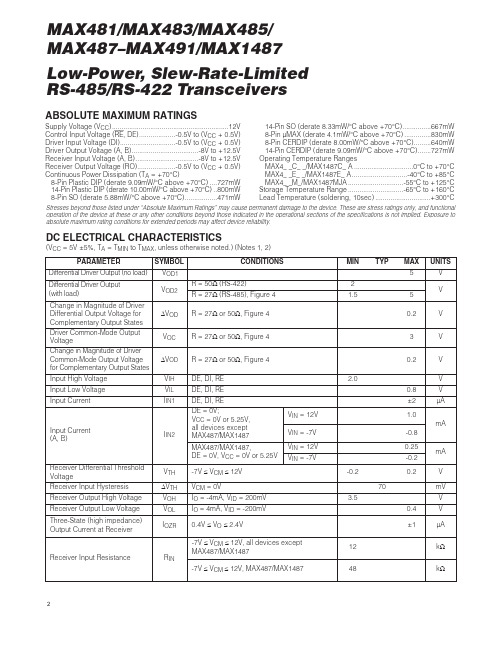
Low-Power, Slew-Rate-Limited RS-485/RS-422 Transceivers2MAX481/MAX483/MAX485/MAX487–MAX491/MAX1487ABSOLUTE MAXIMUM RATINGSSupply Voltage (V CC ) (12V)Control Input Voltage (RE , DE)...................-0.5V to (V CC + 0.5V)Driver Input Voltage (DI).............................-0.5V to (V CC + 0.5V)Driver Output Voltage (A, B)...................................-8V to +12.5VReceiver Input Voltage (A, B).................................-8V to +12.5VReceiver Output Voltage (RO)....................-0.5V to (V CC + 0.5V)Continuous Power Dissipation (T A = +70°C)8-Pin Plastic DIP (derate 9.09mW/°C above +70°C)....727mW14-Pin Plastic DIP (derate 10.00mW/°C above +70°C)..800mW8-Pin SO (derate 5.88mW/°C above +70°C).................471mW 14-Pin SO (derate 8.33mW/°C above +70°C)...............667mW 8-Pin µMAX (derate 4.1mW/°C above +70°C)..............830mW 8-Pin CERDIP (derate 8.00mW/°C above +70°C).........640mW 14-Pin CERDIP (derate 9.09mW/°C above +70°C).......727mW Operating Temperature Ranges MAX4_ _C_ _/MAX1487C_ A...............................0°C to +70°C MAX4__E_ _/MAX1487E_ A.............................-40°C to +85°C MAX4__M_/MAX1487MJA.............................-55°C to +125°C Storage Temperature Range.............................-65°C to +160°C Lead Temperature (soldering, 10sec).............................+300°C DC ELECTRICAL CHARACTERISTICS(V CC = 5V ±5%, T A = T MIN to T MAX , unless otherwise noted.) (Notes 1, 2)Stresses beyond those listed under “Absolute Maximum Ratings” may cause permanent damage to the device. These are stress ratings only, and functional operation of the device at these or any other conditions beyond those indicated in the operational sections of the specifications is not implied. Exposure to absolute maximum rating conditions for extended periods may affect device reliability.V V IN = -7V V IN = 12V V IN = -7V V IN = 12V Input Current (A, B)I IN2V TH k Ω48-7V ≤V CM ≤12V, MAX487/MAX1487R INReceiver Input Resistance -7V ≤V CM ≤12V, all devices exceptMAX487/MAX1487R = 27Ω(RS-485), Figure 40.4V ≤V O ≤2.4VR = 50Ω(RS-422)I O = 4mA, V ID = -200mV I O = -4mA, V ID = 200mV V CM = 0V -7V ≤V CM ≤12V DE, DI, REDE, DI, RE MAX487/MAX1487,DE = 0V, V CC = 0V or 5.25VDE, DI, RE R = 27Ωor 50Ω, Figure 4R = 27Ωor 50Ω, Figure 4R = 27Ωor 50Ω, Figure 4DE = 0V;V CC = 0V or 5.25V,all devices exceptMAX487/MAX1487CONDITIONS k Ω12µA ±1I OZR Three-State (high impedance)Output Current at Receiver V 0.4V OL Receiver Output Low Voltage3.5V OH Receiver Output High VoltagemV 70ΔV TH Receiver Input HysteresisV -0.20.2Receiver Differential ThresholdVoltage-0.2mA 0.25mA -0.81.01.55V OD2Differential Driver Output(with load)V 2V 5V OD1Differential Driver Output (no load)µA ±2I IN1Input Current V 0.8V IL Input Low VoltageV 2.0V IH Input High VoltageV 0.2ΔV OD Change in Magnitude of DriverCommon-Mode Output Voltagefor Complementary Output StatesV 0.2ΔV OD Change in Magnitude of DriverDifferential Output Voltage forComplementary Output StatesV 3V OC Driver Common-Mode OutputVoltageUNITS MIN TYP MAX SYMBOL PARAMETERLow-Power, Slew-Rate-Limited RS-485/RS-422 Transceivers7MAX481/MAX483/MAX485/MAX487–MAX491/MAX1487______________________________________________________________Pin DescriptionFigure 1. MAX481/MAX483/MAX485/MAX487/MAX1487 Pin Configuration and Typical Operating Circuit。
MEMORY存储芯片MT29F1G08ABAEAWP_E中文规格书

General DescriptionMicron NAND Flash devices include an asynchronous data interface for high-perform-ance I/O operations. These devices use a highly multiplexed 8-bit bus (I/Ox) to transfercommands, address, and data. There are five control signals used to implement theasynchronous data interface: CE#, CLE, ALE, WE#, and RE#. Additional signals controlhardware write protection and monitor device status (R/B#).This hardware interface creates a low pin-count device with a standard pinout that re-mains the same from one density to another, enabling future upgrades to higher densi-ties with no board redesign.A target is the unit of memory accessed by a chip enable signal. A target contains one ormore NAND Flash die. A NAND Flash die is the minimum unit that can independentlyexecute commands and report status. A NAND Flash die, in the ONFI specification, isreferred to as a logical unit (LUN). There is at least one NAND Flash die per chip enablesignal. For further details, see Device and Array Organization.Signal Descriptions and AssignmentsTable 1: Asynchronous Signal DefinitionsNotes: 1.See Device and Array Organization for detailed signal connections.2.See Asynchronous Interface Bus Operation for detailed asynchronous interface signaldescriptions.PROGRAM PAGE TWO-PLANE (80h-11h)The PROGRAM PAGE TWO-PLANE (80h-11h) command enables the host to input datato the addressed plane's cache register and queue the cache register to ultimately bemoved to the NAND Flash array. This command can be issued one or more times. Eachtime a new plane address is specified that plane is also queued for data transfer. To in-put data for the final plane and to begin the program operation for all previouslyqueued planes, issue either the PROGRAM PAGE (80h-10h) command or the PROGRAMPAGE CACHE (80h-15h) command. All of the queued planes will move the data to theNAND Flash array. This command is accepted by the die (LUN) when it is ready(RDY = 1).To input a page to the cache register and queue it to be moved to the NAND Flash arrayat the block and page address specified, write 80h to the command register. Unless thiscommand has been preceded by a PROGRAM PAGE TWO-PLANE (80h-11h) command,issuing the 80h to the command register clears all of the cache registers' contents on theselected target. Write five address cycles containing the column address and row ad-dress; data input cycles follow. Serial data is input beginning at the column addressspecified. At any time during the data input cycle, the RANDOM DATA INPUT (85h) andPROGRAM FOR INTERNAL DATA INPUT (85h) commands can be issued. When datainput is complete, write 11h to the command register. The selected die (LUN) will gobusy (RDY = 0, ARDY = 0) for t DBSY.To determine the progress of t DBSY, the host can monitor the target's R/B# signal or,alternatively, the status operations (70h, 78h) can be used. When the LUN's statusshows that it is ready (RDY = 1), additional PROGRAM PAGE TWO-PLANE (80h-11h)commands can be issued to queue additional planes for data transfer. Alternatively, thePROGRAM PAGE (80h-10h) or PROGRAM PAGE CACHE (80h-15h) commands can be is-sued.When the PROGRAM PAGE (80h-10h) command is used as the final command of a two-plane program operation, data is transferred from the cache registers to the NANDFlash array for all of the addressed planes during t PROG. When the die (LUN) is ready(RDY = 1, ARDY = 1), the host should check the status of the FAIL bit for each of theplanes to verify that programming completed successfully.When the PROGRAM PAGE CACHE (80h-15h) command is used as the final commandof a program cache two-plane operation, data is transferred from the cache registers tothe data registers after the previous array operations finish. The data is then movedfrom the data registers to the NAND Flash array for all of the addressed planes. This oc-curs during t CBSY. After t CBSY, the host should check the status of the FAILC bit foreach of the planes from the previous program cache operation, if any, to verify that pro-gramming completed successfully.For the PROGRAM PAGE TWO-PLANE (80h-11h), PROGRAM PAGE (80h-10h), and PRO-GRAM PAGE CACHE (80h-15h) commands, see Two-Plane Operations for two-plane ad-dressing requirements.Erase OperationsErase operations are used to clear the contents of a block in the NAND Flash array toprepare its pages for program operations.Erase OperationsThe ERASE BLOCK (60h-D0h) command, when not preceded by the ERASE BLOCKTWO-PLANE (60h-D1h) command, erases one block in the NAND Flash array. When thedie (LUN) is ready (RDY = 1, ARDY = 1), the host should check the FAIL bit to verify thatthis operation completed successfully.TWO-PLANE ERASE OperationsThe ERASE BLOCK TWO-PLANE (60h-D1h) command can be used to further systemperformance of erase operations by allowing more than one block to be erased in theNAND array. This is done by prepending one or more ERASE BLOCK TWO-PLANE (60h-D1h) commands in front of the ERASE BLOCK (60h-D0h) command. See Two-PlaneOperations for details.ERASE BLOCK (60h-D0h)The ERASE BLOCK (60h-D0h) command erases the specified block in the NAND Flasharray. This command is accepted by the die (LUN) when it is ready (RDY = 1, ARDY = 1).To erase a block, write 60h to the command register. Then write three address cyclescontaining the row address; the page address is ignored. Conclude by writing D0h to thecommand register. The selected die (LUN) will go busy (RDY = 0, ARDY = 0) for t BERSwhile the block is erased.To determine the progress of an ERASE operation, the host can monitor the target'sR/B# signal, or alternatively, the status operations (70h, 78h) can be used. When the die(LUN) is ready (RDY = 1, ARDY = 1) the host should check the status of the FAIL bit.In devices that have more than one die (LUN) per target, during and following inter-leaved die (multi-LUN) operations, the READ STATUS ENHANCED (78h) commandmust be used to select only one die (LUN) for status output. Use of the READ STATUS(70h) command could cause more than one die (LUN) to respond, resulting in bus con-tention.The ERASE BLOCK (60h-D0h) command is used as the final command of an erase two-plane operation. It is preceded by one or more ERASE BLOCK TWO-PLANE (60h-D1h)commands. All blocks in the addressed planes are erased. The host should check thestatus of the operation by using the status operations (70h, 78h). See Two-Plane Opera-tions for two-plane addressing requirements.Figure 46: ERASE BLOCK (60h-D0h) OperationI/O[7:0]RDYInternal Data Move OperationsInternal data move operations make it possible to transfer data within a device fromone page to another using the cache register. This is particularly useful for block man-agement and wear leveling. The INTERNAL DATA MOVE operation is restricted to onlywithin even blocks or only within odd blocks.The INTERNAL DATA MOVE operation is a two-step process consisting of a READ FORINTERNAL DATA MOVE (00h-35h) and a PROGRAM FOR INTERNAL DATA MOVE(85h-10h) command. To move data from one page to another, first issue the READ FORINTERNAL DATA MOVE (00h-35h) command. When the die (LUN) is ready (RDY = 1,ARDY = 1), the host can transfer the data to a new page by issuing the PROGRAM FORINTERNAL DATA MOVE (85h-10h) command. When the die (LUN) is again ready (RDY= 1, ARDY = 1), the host should check the FAIL bit to verify that this operation comple-ted successfully.To prevent bit errors from accumulating over multiple INTERNAL DATA MOVE opera-tions, it is recommended that the host read the data out of the cache register after theREAD FOR INTERNAL DATA MOVE (00h-35h) completes and prior to issuing the PRO-GRAM FOR INTERNAL DATA MOVE (85h-10h) command. The RANDOM DATA READ(05h-E0h) command can be used to change the column address. The host should checkthe data for ECC errors and correct them. When the PROGRAM FOR INTERNAL DATAMOVE (85h-10h) command is issued, any corrected data can be input. The PROGRAMFOR INTERNAL DATA INPUT (85h) command can be used to change the column ad-dress.Between the READ FOR INTERNAL DATA MOVE (00h-35h) and PROGRAM FOR INTER-NAL DATA MOVE (85h-10h) commands, the following commands are supported: statusoperation (70h) and column address operations (05h-E0h, 85h). The RESET operation(FFh) can be issued after READ FOR INTERNAL DATA MOVE (00h-35h), but the con-tents of the cache registers on the target are not valid.READ FOR INTERNAL DATA MOVE (00h-35h)The READ FOR INTERNAL DATA MOVE (00h-35h) command is functionally identical tothe READ PAGE (00h-30h) command, except that 35h is written to the command regis-ter instead of 30h.It is recommended that the host read the data out of the device to verify the data priorto issuing the PROGRAM FOR INTERNAL DATA MOVE (85h-10h) command to preventthe propagation of data errors.。
MUR2100EG;MUR2100ERLG;中文规格书,Datasheet资料

1.0E−07
25°C 1.0E−08
1000
0
200
400
600
800
VR, REVERSE VOLTAGE (V) Figure 4. Typical Reverse Current
1000
PF(AV), AVERAGE POWER DISSIPATION (A)
4.0 3.5 3.0 2.5 2.0 1.5 1.0 0.5
MUR2100E
NOTE 3. − AMBIENT MOUNTING DATA
Data shown for thermal resistance, junction−to−ambient
(RqJA) for the mountings shown is to be used as typical guideline values for preliminary engineering or in case the tie point temperature cannot be measured.
Unit
Maximum Thermal Resistance, Junction−to−Ambient
RqJA (Note 3) °C/W
Stresses exceeding Maximum Ratings may damage the device. Maximum Ratings are stress ratings only. Functional operation above the Recommended Operating Conditions is not implied. Extended exposure to stresses above the Recommended Operating Conditions may affect device reliability. 1. Pulse Test: Pulse Width = 300 ms, Duty Cycle ≤ 2.0%.
m3e飞行参数
温馨小提示:本文主要介绍的是关于m3e飞行参数的文章,文章是由本店铺通过查阅资料,经过精心整理撰写而成。
文章的内容不一定符合大家的期望需求,还请各位根据自己的需求进行下载。
本文档下载后可以根据自己的实际情况进行任意改写,从而已达到各位的需求。
愿本篇m3e飞行参数能真实确切的帮助各位。
本店铺将会继续努力、改进、创新,给大家提供更加优质符合大家需求的文档。
感谢支持!(Thank you for downloading and checking it out!)阅读本篇文章之前,本店铺提供大纲预览服务,我们可以先预览文章的大纲部分,快速了解本篇的主体内容,然后根据您的需求进行文档的查看与下载。
m3e飞行参数(大纲)一、M3E无人机概述1.1M3E无人机简介1.2M3E无人机的主要应用领域二、M3E飞行参数详解2.1飞行器参数2.1.1翼展2.1.2机长2.1.3最大起飞重量2.1.4最大载重2.1.5最大飞行速度2.1.6最大飞行高度2.1.7续航时间2.2动力系统参数2.2.1发动机类型2.2.2电池参数2.2.3驱动电机2.3导航与控制系统参数2.3.1飞行控制系统2.3.2导航系统2.3.3遥控器与地面站2.4传感器与载荷参数2.4.1摄像头2.4.2红外传感器2.4.3多光谱相机2.4.4激光雷达2.4.5其他传感器三、M3E飞行参数优化与调整3.1飞行参数调整方法3.1.1参数调整原则3.1.2参数调整步骤3.2常见飞行参数优化方法3.2.1速度优化3.2.2高度优化3.2.3续航优化3.2.4稳定性能优化四、M3E飞行参数在应用中的注意事项4.1飞行前检查4.1.1飞行器状态检查4.1.2飞行参数确认4.2飞行中监控4.2.1飞行参数实时监控4.2.2异常情况处理4.3飞行后数据分析4.3.1飞行数据记录4.3.2飞行参数分析五、M3E飞行参数在行业应用案例5.1农业植保5.1.1飞行参数设置5.1.2作业效果分析5.2环境监测5.2.1飞行参数设置5.2.2监测成果展示5.3搜索与救援5.3.1飞行参数设置5.3.2救援案例分析一、M3E无人机概述1.1 M3E无人机简介M3E无人机是一款由我国某知名无人机制造商研发的微型无人机。
MEMORY存储芯片MT29F2G08ABAEAWP-IT_E中文规格书

ArchitectureThese devices use NAND Flash electrical and command interfaces. Data, commands,and addresses are multiplexed onto the same pins and received by I/O control circuits.The commands received at the I/O control circuits are latched by a command register and are transferred to control logic circuits for generating internal signals to control de-vice operations. The addresses are latched by an address register and sent to a row de-coder to select a row address, or to a column decoder to select a column address.Data is transferred to or from the NAND Flash memory array, byte by byte (x8) or word by word (x16), through a data register and a cache register.The NAND Flash memory array is programmed and read using page-based operations and is erased using block-based operations. During normal page operations, the data and cache registers act as a single register. During cache operations, the data and cache registers operate independently to increase data throughput. The status register reports the status of die operations.Figure 8: NAND Flash Die (LUN) Functional Block DiagramLOCK Note:1.The LOCK pin is used on the 1.8V device.Figure 15: Asynchronous Data Output Cycles (EDO Mode)CE#RE#I/OxRDYWrite Protect#The write protect# (WP#) signal enables or disables PROGRAM and ERASE operationsto a target. When WP# is LOW, PROGRAM and ERASE operations are disabled. WhenWP# is HIGH, PROGRAM and ERASE operations are enabled.It is recommended that the host drive WP# LOW during power-on until V CC is stable toprevent inadvertent PROGRAM and ERASE operations (see Device Initialization for ad-ditional details).WP# must be transitioned only when the target is not busy and prior to beginning acommand sequence. After a command sequence is complete and the target is ready,WP# can be transitioned. After WP# is transitioned, the host must wait t WW before issu-ing a new command.The WP# signal is always an active input, even when CE# is HIGH. This signal shouldnot be multiplexed with other signals.Ready/Busy#The ready/busy# (R/B#) signal provides a hardware method of indicating whether a tar-get is ready or busy. A target is busy when one or more of its die (LUNs) are busy(RDY = 0). A target is ready when all of its die (LUNs) are ready (RDY = 1). Because eachdie (LUN) contains a status register, it is possible to determine the independent statusof each die (LUN) by polling its status register instead of using the R/B# signal (see Sta-tus Operations for details regarding die (LUN) status).This signal requires a pull-up resistor, Rp, for proper operation. R/B# is HIGH when thetarget is ready, and transitions LOW when the target is busy. The signal's open-draindriver enables multiple R/B# outputs to be OR-tied. Typically, R/B# is connected to an interrupt pin on the system controller.The combination of Rp and capacitive loading of the R/B# circuit determines the rise time of the R/B# signal. The actual value used for Rp depends on the system timing re-quirements. Large values of Rp cause R/B# to be delayed significantly. Between the 10% and 90% points on the R/B# waveform, the rise time is approximately two time con-stants (TC).T C = R × CWhere R = Rp (resistance of pull-up resistor), and C = total capacitive load.The fall time of the R/B# signal is determined mainly by the output impedance of theR/B# signal and the total load capacitance. Approximate Rp values using a circuit load of 100pF are provided in Figure 21 (page 27).The minimum value for Rp is determined by the output drive capability of the R/B# sig-nal, the output voltage swing, and V CC.Rp =V CC (MAX) - V OL (MAX)I OL + ΣILWhere ΣIL is the sum of the input currents of all devices tied to the R/B# pin. Figure 16: READ/BUSY# Open DrainCommand Definitions Table 5: Command SetTable 5: Command Set (Continued)Notes: 1.Busy means RDY = 0.。
- 1、下载文档前请自行甄别文档内容的完整性,平台不提供额外的编辑、内容补充、找答案等附加服务。
- 2、"仅部分预览"的文档,不可在线预览部分如存在完整性等问题,可反馈申请退款(可完整预览的文档不适用该条件!)。
- 3、如文档侵犯您的权益,请联系客服反馈,我们会尽快为您处理(人工客服工作时间:9:00-18:30)。
MUR480E, MUR4100E SWITCHMODE t Power RectifiersUltrafast “E’’ Series with High Reverse Energy CapabilityThese state−of−the−art devices are designed for use in switching power supplies, inverters and as free wheeling diodes.Features•20 mJ Avalanche Energy Guaranteed•Excellent Protection Against V oltage Transients in Switching Inductive Load Circuits•Ultrafast 75 Nanosecond Recovery Time •175°C Operating Junction Temperature •Low Forward V oltage •Low Leakage Current•High Temperature Glass Passivated Junction •Reverse V oltage to 1000 V •These are Pb−Free Devices*Mechanical Characteristics:•Case: Epoxy, Molded•Weight: 1.1 Gram (Approximately)•Finish: All External Surfaces Corrosion Resistant and Terminal Leads are Readily Solderable•Lead Temperature for Soldering Purposes:260°C Max. for 10 Seconds•Shipped in Plastic Bags, 5,000 per Bag•Available Tape and Reel, 1,500 per Reel, by Adding a “RL’’ Suffix to the Part Number•Polarity: Cathode indicated by Polarity BandMAXIMUM RATINGSRatingSymbol ValueUnit Peak Repetitive Reverse Voltage Working Peak Reverse Voltage DC Blocking VoltageMUR480EMUR4100EV RRM V RWM V R 8001000VAverage Rectified Forward Current(Square Wave; Mounting Method #3 Per Note 2)I F(AV) 4.0 @T A = 35°CA Non−Repetitive Peak Surge Current(Surge Applied at Rated Load Conditions Halfwave, Single Phase, 60 Hz)I FSM70AOperating Junction and Storage Temperature RangeT J , T stg−65 to +175°CStresses exceeding Maximum Ratings may damage the device. Maximum Ratings are stress ratings only. Functional operation above the Recommended Operating Conditions is not implied. Extended exposure to stresses above the Recommended Operating Conditions may affect device reliability.*For additional information on our Pb−Free strategy and soldering details, please download the ON Semiconductor Soldering and Mounting Techniques Reference Manual, SOLDERRM/D.ULTRAFAST RECTIFIER 4.0 AMPERES, 800−1000 VOLTSAXIAL LEAD CASE 267STYLE 1A = Assembly LocationMUR4xxx = Device Number (see page 2)YY = Year WW = Work Week G = Pb−Free PackageMARKING DIAGRAMA MUR 4xxx YYWW GG(Note: Microdot may be in either location)See detailed ordering and shipping information on page 2 of this data sheet.ORDERING INFORMATIONTHERMAL CHARACTERISTICSRating Symbol Value Unit Maximum Thermal Resistance, Junction−to−Ambient R q JA See Note 2°C/W ELECTRICAL CHARACTERISTICSCharacteristic Symbol Max UnitMaximum Instantaneous Forward Voltage (Note 1) (i F = 3.0 Amps, T J = 150°C)(i F = 3.0 Amps, T J = 25°C)(i F = 4.0 Amps, T J = 25°C)v F1.531.751.85VMaximum Instantaneous Reverse Current (Note 1) (Rated dc Voltage, T J = 150°C)(Rated dc Voltage, T J = 25°C)i R90025m AMaximum Reverse Recovery Time(I F = 1.0 Amp, di/dt = 50 Amp/m s)(I F = 0.5 Amp, i R = 1.0 Amp, I REC = 0.25 Amp)t rr10075nsMaximum Forward Recovery Time(I F = 1.0 Amp, di/dt = 100 Amp/m s, Recovery to 1.0 V)t fr75ns Controlled Avalanche Energy (See Test Circuit in Figure 6)W AVAL20mJ 1.Pulse Test: Pulse Width = 300 m s, Duty Cycle v2.0%.ORDERING INFORMATIONDevice Marking Package Shipping†MUR420EMUR420E Axial Lead*500 Units / BulkMUR420EG Axial Lead*500 Units / Bulk MUR420ERL Axial Lead*1500 / Tape & Reel MUR420ERLG Axial Lead*1500 / Tape & ReelMUR420ESMUR420ES Axial Lead*500 Units / BulkMUR420ESG Axial Lead*500 Units / BulkMUR4100EMUR4100E Axial Lead*500 Units / BulkMUR4100EG Axial Lead*500 Units / BulkMUR4100ERL Axial Lead*1500 / Tape & ReelMUR4100ERLG Axial Lead*1500 / Tape & Reel†For information on tape and reel specifications, including part orientation and tape sizes, please refer to our Tape and Reel Packaging Specifications Brochure, BRD8011/D.*This package is inherently Pb−Free.MUR480E, MUR4100E, I N S T A N T A N E O U S F O R W A R D C U R R E N T (A M P S )F Figure 4. Power Dissipation I F(AV), AVERAGE FORWARD CURRENT (AMPS)P F (A V )Figure 5. Typical Capacitance, A V E R A G E P O W E R D I S S I P A T I O N (W A T T S )i 10V R , REVERSE VOLTAGE (VOLTS)203050400Figure 6. Test Circuit Figure 7. Current−Voltage WaveformsThe unclamped inductive switching circuit shown in Figure 6 was used to demonstrate the controlled avalanche capability of the new “E’’ series Ultrafast rectifiers. A mercury switch was used instead of an electronic switch to simulate a noisy environment when the switch was being opened.When S1 is closed at t0 the current in the inductor I L ramps up linearly; and energy is stored in the coil. At t1 the switch is opened and the voltage across the diode under test begins to rise rapidly, due to di/dt effects, when this induced voltage reaches the breakdown voltage of the diode, it is clamped at BV DUT and the diode begins to conduct the full load current which now starts to decay linearly through the diode, and goes to zero at t2.By solving the loop equation at the point in time when S1 is opened; and calculating the energy that is transferred to the diode it can be shown that the total energy transferred is equal to the energy stored in the inductor plus a finite amount of energy from the V DD power supply while the diode is in breakdown (from t1 to t2) minus any losses due to finite component resistances. Assuming the component resistive elements are small Equation (1) approximates the total energy transferred to the diode. It can be seen from this equation that if the V DD voltage is low compared to the breakdown voltage of the device, the amount of energy contributed by the supply during breakdown is small and the total energy can be assumed to be nearly equal to the energy stored in the coil during the time when S1 was closed, Equation (2).The oscilloscope picture in Figure 8, shows the information obtained for the MUR8100E (similar die construction as the MUR4100E Series) in this test circuit conducting a peak current of one ampere at a breakdown voltage of 1300 V, and using Equation (2) the energy absorbed by the MUR8100E is approximately 20 mjoules. Although it is not recommended to design for this condition, the new “E’’ series provides added protection against those unforeseen transient viruses that can produce unexplained random failures in unfriendly environments.W AVAL[12LI 2LPKǒBV DUT BV DUT–V DDǓW AVAL[12LI 2LPKFigure 8. Current−Voltage WaveformsCHANNEL 2:I L0.5 AMPS/DIV.CHANNEL 1:V DUT500 VOLTS/DIV.TIME BASE:20 m s/DIV.EQUATION (1): EQUATION (2):NOTE 2 − AMBIENT MOUNTING DATAPACKAGE DIMENSIONSAXIAL LEAD CASE 267−05(DO−201AD)ISSUE GNOTES:1.DIMENSIONING AND TOLERANCING PER ANSI Y14.5M, 1982.2.CONTROLLING DIMENSION: INCH.STYLE 1:PIN 1.CATHODE (POLARITY BAND)2.ANODEDIM MIN MAX MIN MAX MILLIMETERSINCHES A 0.2870.3747.309.50B 0.1890.209 4.80 5.30D 0.0470.051 1.20 1.30K1.000−−−25.40−−−ON Semiconductor and are registered trademarks of Semiconductor Components Industries, LLC (SCILLC). SCILLC reserves the right to make changes without further notice to any products herein. SCILLC makes no warranty, representation or guarantee regarding the suitability of its products for any particular purpose, nor does SCILLC assume any liability arising out of the application or use of any product or circuit, and specifically disclaims any and all liability, including without limitation special, consequential or incidental damages.“Typical” parameters which may be provided in SCILLC data sheets and/or specifications can and do vary in different applications and actual performance may vary over time. All operating parameters, including “Typicals” must be validated for each customer application by customer’s technical experts. SCILLC does not convey any license under its patent rights nor the rights of others. SCILLC products are not designed, intended, or authorized for use as components in systems intended for surgical implant into the body, or other applications intended to support or sustain life, or for any other application in which the failure of the SCILLC product could create a situation where personal injury or death may occur. Should Buyer purchase or use SCILLC products for any such unintended or unauthorized application, Buyer shall indemnify and hold SCILLC and its officers, employees, subsidiaries, affiliates,and distributors harmless against all claims, costs, damages, and expenses, and reasonable attorney fees arising out of, directly or indirectly, any claim of personal injury or death associated with such unintended or unauthorized use, even if such claim alleges that SCILLC was negligent regarding the design or manufacture of the part. SCILLC is an Equal Opportunity/Affirmative Action Employer. This literature is subject to all applicable copyright laws and is not for resale in any manner.PUBLICATION ORDERING INFORMATIONSWITCHMODE is a trademark of Semiconductor Components Industries, LLC.。