chapter1-IC-Test
RTU560 数据表单:二进制输入 23BE40 文件号:1KGT 150 600 V005 1 1

RTU560Data Sheet Binary Input 23BE40Doc.-No.: 1KGT 150 600 V005 1 1Binary Input 23BE40ApplicationThe binary input board 23BE40 is used for the iso-lated input of up to 16 binary process signals. Scan-ning and processing of the inputs are executed with the high time resolution of 1 ms.The board is available in two versions (rubrics):∙ 23BE40 R0011 for 110…125 V DC ∙23BE40 R0012 for 220…250 V DCThe allocation of an input signal to the processing functions can be done according to the rules of con-figuration. The 23BE40 can process the following types of signals:∙ 16 single indications with time stamp ∙ 8 double indications with time stamp∙ 2 step position information each with 8 bit ∙ 8/16 bit digital measured value(s) ∙ 8/16 bit String Information∙16 pulse counters (max. 25Hz)Power supply 560PSU40/ 41 is needed to feed this modules.CharacteristicsAll inputs are potentially isolated by means of opto-couplers. If a common return is necessary, it can be realized by the external short circuit connectors in-cluded in the delivery.The inputs 1 ... 8 feature current sources for oxide film breaking. These current sources are active for 10 ms after applying an input signal. If the input signals change more often than every 30 seconds, then the on-time of the current sources will be re-duced.The input current of type 1.5 mA is chopped for thereduction of the power dissipation. Thus, the average input current is reduced to 0.4 mA. The average input current and the oxide film breaking current are kept constant over the input voltage range.The board has 16 light emitting diodes to indicate the signal-state. The LED’s are organized in two co l-umns. The LED’s follows directly the input.Figure 1:Block diagram 23BE40RTU560Data Sheet Binary Input 23BE402Doc.–No.: 1KGT 150 600 V005 1The binary input board 23BE40 can execute the following processing functions for the different types of signals:∙ Digital filtering to suppress contact bounce ∙ Suppression of technologically caused chat-tering signals∙ Intermediate position suppression and mon-itoring for double indications∙Consistency check for all binary input chan-nels allocated to digital measured valuesThe 23BE40 has a buffer which allows the temporary storage of 50 time-stamped event messages in chronological order designated for transmission to the communication unit.The board’s micro-controller processes all time-critical tasks of the parameterized processing func-tions. Moreover, it carries out the interactive commu-nication with the RTU560 system bus. All configura-tion data and processing parameters are loaded from the communication unit via the RTU560 bus.The board is equipped with a serial interface to the RTU560 system bus.During initialization and operation the board carries out a number of tests. If a fault occurs, it is reported to the communication unit. All fault conditions impair-ing the function of the board are displayed as com-mon fault signal with a light emitting diode (ST). A failure of the board is detected by the communication unit.RTU560Data Sheet Binary Input 23BE40Doc.-No. 1KGT 150 600 V005 1 3Technical DataIn addition to the RTU general technical data, the fol-lowing applies:Mechanical LayoutConnection TypeInsulationElectromagnetic CompatibilityRTU560Data Sheet Binary Input 23BE404Doc.–No.: 1KGT 150 600 V005 1InterferenceSafetyMechanical StressEnvironmental ConditionsOrdering informationNote:We reserve the right to make technical changes or modify the contents of this document without prior notice. With regard to purchase orders, the agreed particulars shall prevail. ABB AG does not accept any responsibility whatsoever for potential er-rors or possible lack of information in this document.We reserve all rights in this document and in the subject matter and illustrations contained therein. Any reproduction, disclosure to third parties or utilization of its contents - in whole or in parts - is forbidden without prior written consent of ABB AG.Copyright© 2012 ABB All rights reserved。
半导体制造技术
Semiconductor Manufacturing Technology半导体制造技术Instructor’s ManualMichael QuirkJulian SerdaCopyright Prentice HallTable of Contents目录OverviewI. Chapter1. Semiconductor industry overview2. Semiconductor materials3. Device technologies—IC families4. Silicon and wafer preparation5. Chemicals in the industry6. Contamination control7. Process metrology8. Process gas controls9. IC fabrication overview10. Oxidation11. Deposition12. Metallization13. Photoresist14. Exposure15. Develop16. Etch17. Ion implant18. Polish19. Test20. Assembly and packagingII. Answers to End-of-Chapter Review QuestionsIII. Test Bank (supplied on diskette)IV. Chapter illustrations, tables, bulleted lists and major topics (supplied on CD-ROM)Notes to Instructors:1)The chapter overview provides a concise summary of the main topics in each chapter.2)The correct answer for each test bank question is highlighted in bold. Test bankquestions are based on the end-of-chapter questions. If a student studies the end-of-chapter questions (which are linked to the italicized words in each chapter), then they will be successful on the test bank questions.2Chapter 1Introduction to the Semiconductor Industry Die:管芯 defective:有缺陷的Development of an Industry•The roots of the electronic industry are based on the vacuum tube and early use of silicon for signal transmission prior to World War II. The first electronic computer, the ENIAC, wasdeveloped at the University of Pennsylvania during World War II.•William Shockley, John Bardeen and Walter Brattain invented the solid-state transistor at Bell Telephone Laboratories on December 16, 1947. The semiconductor industry grew rapidly in the 1950s to commercialize the new transistor technology, with many early pioneers working inSilicon Valley in Northern California.Circuit Integration•The first integrated circuit, or IC, was independently co-invented by Jack Kilby at Texas Instruments and Robert Noyce at Fairchild Semiconductor in 1959. An IC integrates multiple electronic components on one substrate of silicon.•Circuit integration eras are: small scale integration (SSI) with 2 - 50 components, medium scale integration (MSI) with 50 – 5k components, large scale integration (LSI) with 5k to 100kcomponents, very large scale integration (VLSI) with 100k to 1M components, and ultra large scale integration (ULSI) with > 1M components.1IC Fabrication•Chips (or die) are fabricated on a thin slice of silicon, known as a wafer (or substrate). Wafers are fabricated in a facility known as a wafer fab, or simply fab.•The five stages of IC fabrication are:Wafer preparation: silicon is purified and prepared into wafers.Wafer fabrication: microchips are fabricated in a wafer fab by either a merchant chip supplier, captive chip producer, fabless company or foundry.Wafer test: Each individual die is probed and electrically tested to sort for good or bad chips.Assembly and packaging: Each individual die is assembled into its electronic package.Final test: Each packaged IC undergoes final electrical test.•Key semiconductor trends are:Increase in chip performance through reduced critical dimensions (CD), more components per chip (Moore’s law, which predicts the doubling of components every 18-24 months) andreduced power consumption.Increase in chip reliability during usage.Reduction in chip price, with an estimated price reduction of 100 million times for the 50 years prior to 1996.The Electronic Era•The 1950s saw the development of many different types of transistor technology, and lead to the development of the silicon age.•The 1960s were an era of process development to begin the integration of ICs, with many new chip-manufacturing companies.•The 1970s were the era of medium-scale integration and saw increased competition in the industry, the development of the microprocessor and the development of equipment technology. •The 1980s introduced automation into the wafer fab and improvements in manufacturing efficiency and product quality.•The 1990s were the ULSI integration era with the volume production of a wide range of ICs with sub-micron geometries.Career paths•There are a wide range of career paths in semiconductor manufacturing, including technician, engineer and management.2Chapter 2 Characteristics of Semiconductor MaterialsAtomic Structure•The atomic model has three types of particles: neutral neutrons(不带电的中子), positively charged protons(带正电的质子)in the nucleus and negatively charged electrons(带负电的核外电子) that orbit the nucleus. Outermost electrons are in the valence shell, and influence the chemical and physical properties of the atom. Ions form when an atom gains or loses one or more electrons.The Periodic Table•The periodic table lists all known elements. The group number of the periodic table represents the number of valence shell electrons of the element. We are primarily concerned with group numbers IA through VIIIA.•Ionic bonds are formed when valence shell electrons are transferred from the atoms of one element to another. Unstable atoms (e.g., group VIIIA atoms because they lack one electron) easily form ionic bonds.•Covalent bonds have atoms of different elements that share valence shell electrons.3Classifying Materials•There are three difference classes of materials:ConductorsInsulatorsSemiconductors•Conductor materials have low resistance to current flow, such as copper. Insulators have high resistance to current flow. Capacitance is the storage of electrical charge on two conductive plates separated by a dielectric material. The quality of the insulation material between the plates is the dielectric constant. Semiconductor materials can function as either a conductor or insulator.Silicon•Silicon is an elemental semiconductor material because of four valence shell electrons. It occurs in nature as silica and is refined and purified to make wafers.•Pure silicon is intrinsic silicon. The silicon atoms bond together in covalent bonds, which defines many of silicon’s properties. Silicon atoms bond together in set, repeatable patterns, referred to asa crystal.•Germanium was the first semiconductor material used to make chips, but it was soon replaced by silicon. The reasons for this change are:Abundance of siliconHigher melting temperature for wider processing rangeWide temperature range during semiconductor usageNatural growth of silicon dioxide•Silicon dioxide (SiO2) is a high quality, stable electrical insulator material that also serves as a good chemical barrier to protect silicon from external contaminants. The ability to grow stable, thin SiO2 is fundamental to the fabrication of Metal-Oxide-Semiconductor (MOS) devices. •Doping increases silicon conductivity by adding small amounts of other elements. Common dopant elements are from trivalent, p-type Group IIIA (boron) and pentavalent, n-type Group VA (phosphorus, arsenic and antimony).•It is the junction between the n-type and p-type doped regions (referred to as a pn junction) that permit silicon to function as a semiconductor.4Alternative Semiconductor Materials•The alternative semiconductor materials are primarily the compound semiconductors. They are formed from Group IIIA and Group VA (referred to as III-V compounds). An example is gallium arsenide (GaAs).•Some alternative semiconductors come from Group IIA and VIA, referred to as II-VI compounds. •GaAs is the most common III-V compound semiconductor material. GaAs ICs have greater electron mobility, and therefore are faster than ICs made with silicon. GaAs ICs also have higher radiation hardness than silicon, which is better for space and military applications. The primary disadvantage of GaAs is the lack of a natural oxide.5Chapter 3Device TechnologiesCircuit Types•There are two basic types of circuits: analog and digital. Analog circuits have electrical data that varies continuously over a range of voltage, current and power values. Digital circuits have operating signals that vary about two distinct voltage levels – a high and a low.Passive Component Structures•Passive components such as resistors and capacitors conduct electrical current regardless of how the component is connected. IC resistors are a passive component. They can have unwanted resistance known as parasitic resistance. IC capacitor structures can also have unintentional capacitanceActive Component Structures•Active components, such as diodes and transistors can be used to control the direction of current flow. PN junction diodes are formed when there is a region of n-type semiconductor adjacent to a region of p-type semiconductor. A difference in charge at the pn junction creates a depletion region that results in a barrier voltage that must be overcome before a diode can be operated. A bias voltage can be configured to have a reverse bias, with little or no conduction through the diode, or with a forward bias, which permits current flow.•The bipolar junction transistor (BJT) has three electrodes and two pn junctions. A BJT is configured as an npn or pnp transistor and biased for conduction mode. It is a current-amplifying device.6• A schottky diode is formed when metal is brought in contact with a lightly doped n-type semiconductor material. This diode is used in faster and more power efficient BJT circuits.•The field-effect transistor (FET), a voltage-amplifying device, is more compact and power efficient than BJT devices. A thin gate oxide located between the other two electrodes of the transistor insulates the gate on the MOSFET. There are two categories of MOSFETs, nMOS (n-channel) and pMOS (p-channel), each which is defined by its majority current carriers. There is a biasing scheme for operating each type of MOSFET in conduction mode.•For many years, nMOS transistors have been the choice of most IC manufacturers. CMOS, with both nMOS and pMOS transistors in the same IC, has been the most popular device technology since the early 1980s.•BiCMOS technology makes use of the best features of both CMOS and bipolar technology in the same IC device.•Another way to categorize FETs is in terms of enhancement mode and depletion mode. The major different is in the way the channels are doped: enhancement-mode channels are doped opposite in polarity to the source and drain regions, whereas depletion mode channels are doped the same as their respective source and drain regions.Latchup in CMOS Devices•Parasitic transistors can create a latchup condition(???????) in CMOS ICs that causes transistors to unintentionally(无心的) turn on. To control latchup, an epitaxial layer is grown on the wafer surface and an isolation barrier(隔离阻障)is placed between the transistors. An isolation layer can also be buried deep below the transistors.Integrated Circuit Productsz There are a wide range of semiconductor ICs found in electrical and electronic products. This includes the linear IC family, which operates primarily with anal3og circuit applications, and the digital IC family, which includes devices that operate with binary bits of data signals.7Chapter 4Silicon and Wafer Preparation8z Semiconductor-Grade Silicon•The highly refined silicon used for wafer fabrication is termed semiconductor-grade silicon (SGS), and sometimes referred to as electronic-grade silicon. The ultra-high purity of semiconductor-grade silicon is obtained from a multi-step process referred to as the Siemens process.Crystal Structure• A crystal is a solid material with an ordered, 3-dimensional pattern over a long range. This is different from an amorphous material that lacks a repetitive structure.•The unit cell is the most fundamental entity for the long-range order found in crystals. The silicon unit cell is a face-centered cubic diamond structure. Unit cells can be organized in a non-regular arrangement, known as a polycrystal. A monocrystal are neatly arranged unit cells.Crystal Orientation•The orientation of unit cells in a crystal is described by a set of numbers known as Miller indices.The most common crystal planes on a wafer are (100), (110), and (111). Wafers with a (100) crystal plane orientation are most common for MOS devices, whereas (111) is most common for bipolar devices.Monocrystal Silicon Growth•Silicon monocrystal ingots are grown with the Czochralski (CZ) method to achieve the correct crystal orientation and doping. A CZ crystal puller is used to grow the silicon ingots. Chunks of silicon are heated in a crucible in the furnace of the puller, while a perfect silicon crystal seed is used to start the new crystal structure.• A pull process serves to precisely replicate the seed structure. The main parameters during the ingot growth are pull rate and crystal rotation. More homogeneous crystals are achieved with a magnetic field around the silicon melt, known as magnetic CZ.•Dopant material is added to the melt to dope the silicon ingot to the desired electrical resistivity.Impurities are controlled during ingot growth. A float-zone crystal growth method is used toachieve high-purity silicon with lower oxygen content.•Large-diameter ingots are grown today, with a transition underway to produce 300-mm ingot diameters. There are cost benefits for larger diameter wafers, including more die produced on a single wafer.Crystal Defects in Silicon•Crystal defects are interruptions in the repetitive nature of the unit cell. Defect density is the number of defects per square centimeter of wafer surface.•Three general types of crystal defects are: 1) point defects, 2) dislocations, and 3) gross defects.Point defects are vacancies (or voids), interstitial (an atom located in a void) and Frenkel defects, where an atom leaves its lattice site and positions itself in a void. A form of dislocation is astacking fault, which is due to layer stacking errors. Oxygen-induced stacking faults are induced following thermal oxidation. Gross defects are related to the crystal structure (often occurring during crystal growth).Wafer Preparation•The cylindrical, single-crystal ingot undergoes a series of process steps to create wafers, including machining operations, chemical operations, surface polishing and quality checks.•The first wafer preparation steps are the shaping operations: end removal, diameter grinding, and wafer flat or notch. Once these are complete, the ingot undergoes wafer slicing, followed by wafer lapping to remove mechanical damage and an edge contour. Wafer etching is done to chemically remove damage and contamination, followed by polishing. The final steps are cleaning, wafer evaluation and packaging.Quality Measures•Wafer suppliers must produce wafers to stringent quality requirements, including: Physical dimensions: actual dimensions of the wafer (e.g., thickness, etc.).Flatness: linear thickness variation across the wafer.Microroughness: peaks and valleys found on the wafer surface.Oxygen content: excessive oxygen can affect mechanical and electrical properties.Crystal defects: must be minimized for optimum wafer quality.Particles: controlled to minimize yield loss during wafer fabrication.Bulk resistivity(电阻系数): uniform resistivity from doping during crystal growth is critical. Epitaxial Layer•An epitaxial layer (or epi layer) is grown on the wafer surface to achieve the same single crystal structure of the wafer with control over doping type of the epi layer. Epitaxy minimizes latch-up problems as device geometries continue to shrink.Chapter 5Chemicals in Semiconductor FabricationEquipment Service Chase Production BayChemical Supply Room Chemical Distribution Center Holding tank Chemical drumsProcess equipmentControl unit Pump Filter Raised and perforated floorElectronic control cablesSupply air ductDual-wall piping for leak confinement PumpFilterChemical control and leak detection Valve boxes for leak containment Exhaust air ductStates of Matter• Matter in the universe exists in 3 basic states (宇宙万物存在着三种基本形态): solid, liquid andgas. A fourth state is plasma.Properties of Materials• Material properties are the physical and chemical characteristics that describe its unique identity.• Different properties for chemicals in semiconductor manufacturing are: temperature, pressure andvacuum, condensation, vapor pressure, sublimation and deposition, density, surface tension, thermal expansion and stress.Temperature is a measure of how hot or cold a substance is relative to another substance. Pressure is the force exerted per unit area. Vacuum is the removal of gas molecules.Condensation is the process of changing a gas into a liquid. Vaporization is changing a liquidinto a gas.Vapor pressure is the pressure exerted by a vapor in a closed container at equilibrium.Sublimation is the process of changing a solid directly into a gas. Deposition is changing a gas into a solid.Density is the mass of a substance divided by its volume.Surface tension of a liquid is the energy required to increase the surface area of contact.Thermal expansion is the increase in an object’s dimension due to heating.Stress occurs when an object is exposed to a force.Process Chemicals•Semiconductor manufacturing requires extensive chemicals.• A chemical solution is a chemical mixture. The solvent is the component of the solution present in larger amount. The dissolved substances are the solutes.•Acids are solutions that contain hydrogen and dissociate in water to yield hydronium ions. A base is a substance that contains the OH chemical group and dissociates in water to yield the hydroxide ion, OH-.•The pH scale is used to assess the strength of a solution as an acid or base. The pH scale varies from 0 to 14, with 7 being the neutral point. Acids have pH below 7 and bases have pH values above 7.• A solvent is a substance capable of dissolving another substance to form a solution.• A bulk chemical distribution (BCD) system is often used to deliver liquid chemicals to the process tools. Some chemicals are not suitable for BCD and instead use point-of-use (POU) delivery, which means they are stored and used at the process station.•Gases are generally categorized as bulk gases or specialty gases. Bulk gases are the relatively simple gases to manufacture and are traditionally oxygen, nitrogen, hydrogen, helium and argon.The specialty gases, or process gases, are other important gases used in a wafer fab, and usually supplied in low volume.•Specialty gases are usually transported to the fab in metal cylinders.•The local gas distribution system requires a gas purge to flush out undesirable residual gas. Gas delivery systems have special piping and connections systems. A gas stick controls the incoming gas at the process tool.•Specialty gases may be classified as hydrides, fluorinated compounds or acid gases.Chapter 6Contamination Control in Wafer FabsIntroduction•Modern semiconductor manufacturing is performed in a cleanroom, isolated from the outside environment and contaminants.Types of contamination•Cleanroom contamination has five categories: particles, metallic impurities, organic contamination, native oxides and electrostatic discharge. Killer defects are those causes of failure where the chip fails during electrical test.Particles: objects that adhere to a wafer surface and cause yield loss. A particle is a killer defect if it is greater than one-half the minimum device feature size.Metallic impurities: the alkali metals found in common chemicals. Metallic ions are highly mobile and referred to as mobile ionic contaminants (MICs).Organic contamination: contains carbon, such as lubricants and bacteria.Native oxides: thin layer of oxide growth on the wafer surface due to exposure to air.Electrostatic discharge (ESD): uncontrolled transfer of static charge that can damage the microchip.Sources and Control of Contamination•The sources of contamination in a wafer fab are: air, humans, facility, water, process chemicals, process gases and production equipment.Air: class number designates the air quality inside a cleanroom by defining the particle size and density.Humans: a human is a particle generator. Humans wear a cleanroom garment and follow cleanroom protocol to minimize contamination.Facility: the layout is generally done as a ballroom (open space) or bay and chase design.Laminar airflow with air filtering is used to minimize particles. Electrostatic discharge iscontrolled by static-dissipative materials, grounding and air ionization.Ultrapure deiniozed (DI) water: Unacceptable contaminants are removed from DI water through filtration to maintain a resistivity of 18 megohm-cm. The zeta potential represents a charge on fine particles in water, which are trapped by a special filter. UV lamps are used for bacterial sterilization.Process chemicals: filtered to be free of contamination, either by particle filtration, microfiltration (membrane filter), ultrafiltration and reverse osmosis (or hyperfiltration).Process gases: filtered to achieve ultraclean gas.Production equipment: a significant source of particles in a fab.Workstation design: a common layout is bulkhead equipment, where the major equipment is located behind the production bay in the service chase. Wafer handling is done with robotic wafer handlers. A minienvironment is a localized environment where wafers are transferred on a pod and isolated from contamination.Wafer Wet Cleaning•The predominant wafer surface cleaning process is with wet chemistry. The industry standard wet-clean process is the RCA clean, consisting of standard clean 1 (SC-1) and standard clean 2 (SC-2).•SC-1 is a mixture of ammonium hydroxide, hydrogen peroxide and DI water and capable of removing particles and organic materials. For particles, removal is primarily through oxidation of the particle or electric repulsion.•SC-2 is a mixture of hydrochloric acid, hydrogen peroxide and DI water and used to remove metals from the wafer surface.•RCA clean has been modified with diluted cleaning chemistries. The piranha cleaning mixture combines sulfuric acid and hydrogen peroxide to remove organic and metallic impurities. Many cleaning steps include an HF last step to remove native oxide.•Megasonics(兆声清洗) is widely used for wet cleaning. It has ultrasonic energy with frequencies near 1 MHz. Spray cleaning will spray wet-cleaning chemicals onto the wafer. Scrubbing is an effective method for removing particles from the wafer surface.•Wafer rinse is done with overflow rinse, dump rinse and spray rinse. Wafer drying is done with spin dryer or IPA(异丙醇) vapor dry (isopropyl alcohol).•Some alternatives to RCA clean are dry cleaning, such as with plasma-based cleaning, ozone and cryogenic aerosol cleaning.Chapter 7Metrology and Defect InspectionIC Metrology•In a wafer fab, metrology refers to the techniques and procedures for determining physical and electrical properties of the wafer.•In-process data has traditionally been collected on monitor wafers. Measurement equipment is either stand-alone or integrated.•Yield is the percent of good parts produced out of the total group of parts started. It is an indicator of the health of the fabrication process.Quality Measures•Semiconductor quality measures define the requirements for specific aspects of wafer fabrication to ensure acceptable device performance.•Film thickness is generally divided into the measurement of opaque film or transparent film. Sheet resistance measured with a four-point probe is a common method of measuring opaque films (e.g., metal film). A contour map shows sheet resistance deviations across the wafer surface.•Ellipsometry is a nondestructive, noncontact measurement technique for transparent films. It works based on linearly polarized light that reflects off the sample and is elliptically polarized.•Reflectometry is used to measure a film thickness based on how light reflects off the top and bottom surface of the film layer. X-ray and photoacoustic technology are also used to measure film thickness.•Film stress is measured by analyzing changes in the radius of curvature of the wafer. Variations in the refractive index are used to highlight contamination in the film.•Dopant concentration is traditionally measured with a four-point probe. The latest technology is the thermal-wave system, which measures the lattice damage in the implanted wafer after ion implantation. Another method for measuring dopant concentration is spreading resistance probe. •Brightfield detection is the traditional light source for microscope equipment. An optical microscope uses light reflection to detect surface defects. Darkfield detection examines light scattered off defects on the wafer surface. Light scattering uses darkfield detection to detectsurface particles by illuminating the surface with laser light and then using optical imaging.•Critical dimensions (CDs) are measured to achieve precise control over feature size dimensions.The scanning electron microscope is often used to measure CDs.•Conformal step coverage is measured with a surface profiler that has a stylus tip.•Overlay registration measures the ability to accurately print photoresist patterns over a previously etched pattern.•Capacitance-voltage (C-V) test is used to verify acceptable charge conditions and cleanliness at the gate structure in a MOS device.Analytical Equipment•The secondary-ion mass spectrometry (SIMS) is a method of eroding a wafer surface with accelerated ions in a magnetic field to analyze the surface material composition.•The atomic force microscope (AFM) is a surface profiler that scans a small, counterbalanced tip probe over the wafer to create a 3-D surface map.•Auger electron spectroscopy (AES) measures composition on the wafer surface by measuring the energy of the auger electrons. It identifies elements to a depth of about 2 nm. Another instrument used to identify surface chemical species is X-ray photoelectron spectroscopy (XPS).•Transmission electron microscopy (TEM) uses a beam of electrons that is transmitted through a thin slice of the wafer. It is capable of quantifying very small features on a wafer, such as silicon crystal point defects.•Energy-dispersive spectrometer (EDX) is a widely used X-ray detection method for identifying elements. It is often used in conjunction with the SEM.• A focused ion beam (FIB) system is a destructive technique that focuses a beam of ions on the wafer to carve a thin cross section from any wafer area. This permits analysis of the wafermaterial.Chapter 8Gas Control in Process ChambersEtch process chambers••The process chamber is a controlled vacuum environment where intended chemical reactions take place under controlled conditions. Process chambers are often configured as a cluster tool. Vacuum•Vacuum ranges are low (rough) vacuum, medium vacuum, high vacuum and ultrahigh vacuum (UHV). When pressure is lowered in a vacuum, the mean free path(平均自由行程) increases, which is important for how gases flow through the system and for creating a plasma.Vacuum Pumps•Roughing pumps are used to achieve a low to medium vacuum and to exhaust a high vacuum pump. High vacuum pumps achieve a high to ultrahigh vacuum.•Roughing pumps are dry mechanical pumps or a blower pump (also referred to as a booster). Two common high vacuum pumps are a turbomolecular (turbo) pump and cryopump. The turbo pump is a reliable, clean pump that works on the principle of mechanical compression. The cryopump isa capture pump that removes gases from the process chamber by freezing them.。
IC test

目的:利用离子色谱仪来测定驱动器零件在生产过程中被污染的程度使用仪器:DX-120离子色谱仪1.0程序1.1 分析前准备1.1.1 开启Milli-Q,2~3分钟,慢流1.1.2 检查水质达到18.2MQ才可使用。
1.1.3 每天更换阴,阳离子洗脱液,详情如下:Anion:(2.7mM Na2CO3+ 0.3mM NaHCO3)加超纯水至1LCation: 20mM Methanesulfonic acid 加超纯水至1L以上试药需要在过滤装置上过滤。
1.1.3 用干凈的镊子取样品放在冲洗过的烧杯里,装DI水确保充分浸泡,(vol/Area=1)在恒温水浴振荡器上800C±50C恒温1小时。
1.1.4 从电炉上移开然后直接用冲洗过的镊子取出零件,把盖子放回原处(盖上盖子)允许样品冷却到室温.1.1.5 用相同的容器装相同体积的水在同样在条件下加热,作为Blank.1.2 开机操作1.2.1 开启计算机,打开Chromeleon .1.2.2 开AS40自动取样器后面的电源开关1.2.3 十秒钟后开DX-120前面板左下角的电源开关1.2.4 打开IC机旁的氮气瓶,调出口压力为0.5Mpa.1.2.5 按IC机前面板的Eluent pressure,接着按Pump,1.2.6 拧松废液阀,按SRS键。
1.2.7 选择所需的Column,调节IC机箱内侧压力传感器旋扭(即调节泵的流速)。
1.3 分析操作程序1.3.1 运行样品1.3.1 当泵运行30分钟以后观察DX_120_Column_mode_As40.pan窗口基线是否平衡,如果未平衡就要继续运行。
1.3.2 稳定后,装浸泡的溶液到自动取样瓶。
1.3.3 装三个标准液,一个空白,样品1.3.4 准备好后,按AS40前面板上的RUN.1.3.5 再在DX_120_Column_mode_As40.pan窗口中Bench下选择Start.然后在Add下选中建立的Sequence,最后按OK.1.4数据处理1.4.1 标准液校正1.4.1.1运行完后,观察分析结果是否与STD Solution相吻合,如果分析结果误差小于+10%,说明分析结果正确。
DC_TEST
F1
K1 K2 K3 optional
ST
Current Load
(Outputs)
F2
Voltage Receiver
(Outputs)
PMU Connection High Speed Current Comparators
Vout Comparators + Force Sense + -
+ -
Current Range
1 μA 8 μA 64μA 512μA 4mA 32mA 256mA
Current Accuracy
±(0.5%+5.12nΑ) ±(0.5%+6.40nΑ) ±(0.5%+12.8nΑ) ±(0.5%+65.5nΑ) ±(0.5%+512nΑ) ±(0.5%+4.09μΑ) ±(0.5%+32.7μΑ)
B a sic T e r m s
T e r m s th a t A p p ly to th e D U T (s ig n a l p in s )
S ig n a l P in s Inp u t, o u tp u t, T ri– S ta te ® a nd bi– d ire c tio na l p ins (p o w e r a nd g ro u nd p ins are no t inclu d e d in this d e finitio n). S ig nal p ins have a stru c tu re w hic h is d iffe re nt fro m p o w e r p ins. A d e vice p in that acts as a bu ffe r b e tw e e n e x te rna l sig na ls a n d the inte rna l lo g ic o f a d e v ic e . T he inp u t se n se s the v o lta g e a p p lie d to it a nd tra nsm its a lo g ic 0 o r lo g ic 1 le ve l to the inte rna l lo g ic o f the d e vic e . A d e v ic e p in tha t a c ts a s a b u ffe r b e tw e e n the inte rna l lo g ic o f a d e vice and the exte rnal enviro nm ent. A n o u tp u t p in p ro vid es the c o rre c t vo lta g e s to p ro d u c e a lo g ic 0 o r lo g ic 1 le ve l a nd a lso su p p lie s the IO L /IO H c u rre nt.
hypersensitivity.Detection 免疫学 超敏反应

Mold Spores 霉菌孢子 Animal Hair and Dander 动物毛及皮屑
(ii) Ab: IgE 1.Generation of IgE
Th1: IL-2,IFN-g,TNF-b, IL-12 Th2: IL-4,5,6,10,13 IL-4→B→IgE
(IFN-g inhibit IL-4) (IL-12 inhibit IgE)
输血反应
ABO blood groups and serum antibodies
blood group (phenotype)
genotype AA, AO
antigen A
serum antibody Anti-B
A
B
AB O
BB, BO
AB OO
B
A and B H
Anti-A
None Anti-A Anti-B
Type Ⅲ Hypersensitivity
(IC mediated, vasculitis type血管炎型)
一、Pathogenesis: (一) IC formation and deletion:
1.Size of IC:
①soluble Ag ②IgG(mainly) ③Ag Ab Ratio: Ag : Ab Ag>>Ab Ag = Ab Ag<<Ab Ag > Ab
Hypersensitivity 超敏反应
(Allergy, 变态反应) (Anaphylaxis, 过敏反应)
Chapter 20
Concept
• Allergen (Anaphylactogen) 过敏原 secondly enter sensitized host.
医学英语文献阅读一(1-8词汇)

A reading course IChapter1TextAprematurely 过早地diagnosis 诊断sub health 亚健康immune system 免疫系统respectively 分别地prevalent 普遍地spearhead 为…带头,为…先锋sustained 可持续的intellectual 知识分子transitional 过度的chronic 慢性的infectious传染的massage 按摩,推拿blood circulation 血液循环textBdefect 缺点,缺陷abnormality 畸形,异常cardiac 心脏的,心脏病的cardiac arrest 心搏停止screening test 筛选试验,屏蔽试验coroner 验尸官autopsy 验尸,尸体解剖ventricular 心室的,脑室的fibrillation 纤维性颤动ventricular fibrillation 心室纤维性颤动hypertrophic 肥厚的cardiomyopathy 心肌症hypertrophic cardiomyopathy 肥大型心肌病myocardium 心肌,心肌层coronary 冠状的artery 动脉compress 压缩,压紧syndrome 综合征inherit 继承,遗传chaotic 混乱的,无秩序的erratic 不稳定的,古怪的commotia cordis 心脏震动red flag 危险信号on the outlook 寻找,警惕着syncope 晕厥exertion 努力,用力seizures 癫痫,痉挛screening 筛选asthma 哮喘,气喘implantable 可移植的,可植入的cardioverter 心律转变器,复律器defibrillator 去纤颤器,电震发生器pacemaker 心律调整器,起搏器arrhythmia 心律不齐,心律失常electrocardiogram 心电图Vocabularysub health亚健康massage 按摩,推拿diagnosis 诊断suffernegativeaccelerateinfectioncirculationhealthcaredefectinheritcardiactriggerabnormalitysurgeryscreeningsignaldisordersyndromeprematurechapter2TextAdrug resistance耐药性Aids 艾滋病tuberculosis 肺结核malaria 疟疾scourge 灾祸,苦难的根源penicillin 盘尼西林antibiotic 抗菌素incentive 动机,刺激institution 公共机构,习俗leadership 领导能力,领导surveillance 监督,监视priority 优先,优先权,优先考虑的事hygience 卫生,卫生学lancet 小刀,柳叶刀haemorrhage 大出血tranexamic acid 氨甲环酸malnutrition 营养不良soaring 高耸的,猛增的depletion 消耗,放血stock 库存,血统textBallergy 过敏症,反感allergic 对…过敏/极讨厌的side effect 副作用sulfa 磺胺的,磺胺药剂的immune 免疫的offending 不愉快的medication 药物,药物治疗adverse 不利的,相反的itchy 发痒的,渴望的rash 皮疹hives 荨麻疹,假膜性喉头炎exposure 暴露,揭露anaphylaxis 过敏性,过敏性反应prescription 药方,指示symptom 征兆,症状wheeze 喘息serum 血清,浆液injection 注射,注射剂foreign 外国的,异质的medical facilities 医疗设施latex 乳胶,乳液application 应用,敷用amoxicillin 阿莫西林,氢氨苄青霉素ampicillin 氨苄西林,氨苄青霉素augmentin 安灭菌,奥格门汀carbenicillin 羧苄青霉素dicloxacillin 双氯西林,双氯青霉素cephalosporin 头孢菌素cefaclor 头孢克洛,氯氨苄青霉素cefadroxil 头孢氢氨苄cefepime 头孢吡肟cefprozil 头孢丙烯cephradine 头孢拉啶,先锋霉素cephalexin 头孢氨苄sulfasalazine 柳氮磺胺吡啶Bactrim 复方新诺明sulfate 硫酸盐insulin 胰岛素manifest 证明,表明iodine 碘,碘酒bloodstream 血液,血液的流动vessel 脉管,血管nausea 恶心,晕船,极端的憎恶vomit 呕吐,吐出dizziness 头晕,头昏眼花Vocabularysymptioninsulinsurveillancedizzinessimmuneallergicresistancemalariasulfaantibioticitchyforeignvomitbloodstreaminjectionhygieneprescriptionasthmahealthcareanaphylaxicchapter3textAhospice 临终关怀,临终关怀医院catch on 变得流行terminally 不治地,晚期地allusion 暗示,提及influential 有影响的decent 体面的,像样的prolong 延长,拖延existence 生存,生活intervention 干预,介入hostile 敌对的,怀敌意的dedicate 致力,献身explicit 明确的,清楚的intervene 干涉,插入palliative 缓和剂,暂时姑息outstrip 超过,胜过expectancy 期望,期待predictable 可预言的geriatrics 老年病学,老年病人succumb屈服,被压垮dementia 痴呆decay 衰败,衰退textBswallow 吞下,咽下stressful 紧张的,有压力的appreciate 欣赏,感激pursue 继续,从事alternative 选择,替换物available 可得到的,可利用的caregiver 照料者,护理者mission 使命,任务knowledgeable 知识渊博的,有见识的approach 接近expertise 专门知识,专家意见incredibly难以置信地distress 使悲痛,使贫困anticipate 预期,期望compassionate 慈悲的,富于同情心的participation 参与,分享excel 优于,胜过,擅长Vocabularyimmortalterminaldementiahospicedecentanxiousexpectancycaregiverpositiveapproachguidancepursuemissioninterventionemotionalalternativegrievefuneralphysicaltubechapter4textAface lift 面部拉皮手术deposit 沉积物cosmetic 美容的,化妆用的endoscopic 内窥镜的,用内窥镜检查的incision 切口,切割contour 轮廓,周线bandage 绷带wrinkle 皱纹crease 折痕,皱纹swelling 肿胀,增大restrict 限制,约束minimal 最小限度的,极小的invasive 侵略性的,攻击性的invasive surgery 侵入性外科手术anesthesia 麻醉sedation 镇静的,镇静剂visibe 明显的,看得见的temple 太阳穴textBlaser 激光remedy 补救,治疗hyperpigmentation 色素沉着过度discolor 使变色,使褪色discoloration 变色dermabrasion 磨去皮肤疤痕之手术,磨皮手术acne 痤疮,粉刺ablative 烧蚀的vaporize 汽化,使…蒸发downtime 停工期collagen 胶原,胶原蛋白pulse 脉冲,脉动rejuvenation 返老还童,恢复活动sagging 松垂的,下沉的vascular 血管的,淋巴管的lesion 病变,损伤antiviral 抗病毒物质antibacterial 抗菌剂,抗菌药yeast 酵母complication 并发症intravenous 静脉内的penetrate 渗透,穿透ointment 药膏,软膏petroleum jelly 凡士林,矿油temporary 暂时的,短暂的dormant 休眠的,静止的herpes 疱疹Vocabularyendoscopicmedicationcomplicationantiviralwrinkleanesthesiavascularswellingexposurehyperpigmentationscarinvasiveintravenouspeeldermabrasiondormantincisiondepositlesioncollagenchapter5textAgenetic 遗传的,基因的loom 可怕地出现,令人惊恐的隐现invade 侵入,侵略staple 主要的,常用的biotechnologist 生物工艺学家estimate 估计ingredient 材料,原料reveal 显示,透漏domesticated 家养的toxicity 毒性,毒性作用,毒性反应allergenicity 变应原性,过敏反应antibiotic 抗生的,抗菌的extinction 灭绝hazardous 有危险的,冒险的tangle 纠纷,混乱状态anomaly 异常,反常事物jurisdiction 管辖权haphazard 随便的,无计划的contaminate 污染,弄脏legislation 立法negligence 疏忽,忽视biotechnology 生物技术,生物工艺学textBaccess 使用权,接近或享用的机会temporarily 临时地affordable 负担得起的shortage 缺乏utilize 使用,利用household 家庭的,日常的intellectually 智力上,理智地resource 资源effective 有效的fertilizer 化肥productive 能生产的,多生产的deterioration 恶化undertake 承担,从事resistance 抵抗,反抗cultivate 培养,耕作cubic 立方体的,立方irrigation 灌溉salinisation 盐渍化consequently 因此,结果enhance 提高,加强invest 投资cyclone 旋风,气旋,飓风flee 逃走,消失,消失debris 碎片,残骸prioritise 给予…优先权,按优先顺序处理quarantine 检疫tariff 关税表,收费表subsidise 资助给…补助金deprive使丧失,剥夺Vocabularyorganismtanglecondimentfertilizershortagecontaminateanomalydebrisbacteriaregulateaccesstariffingredientprioritiseextinctiondeteriorationhaphazardirrigationpandemicutilizationchapter6textAwillpower 意志力,毅力illicit 违法的,非法的staggering令人惊讶的deleterious 有毒的,有害的disintegration 分解,瓦解chronic 慢性的,长期的relapse 旧病复发,故态复萌counteract 抵消,中和disruptive 破坏的,分裂性的psychiatric 精神病学的,精神病治疗的diabetes 糖尿病,多尿症reinstate 使恢复,使复原textBgay teen 同性恋青少年acute 严重的,急性的lesbian 女同性恋bisexual 双性恋的transgender 跨性别者,变性人heterosexual 异性的,异性恋的subgroup 子群straight teen 异性恋青少年,非同性恋青少年homophobia 对同性恋的恐惧,对同性恋的憎恶victimization 欺骗,侵害disparity 不同,不一致marginalize 排斥,使处于社会边缘nongovernmental 非政府的harassment 骚扰,烦恼marijuana 大麻,大麻毒品cocaine 可卡因methamphetamine 甲基苯丙胺,冰毒assault 攻击,袭击pseudonym 笔名,假名stigmatization 污辱adolescent 青少年prognosis 预后,预知grim 冷酷的,糟糕的homophobic害怕同性恋的imperative 必要的,紧急的confidential 表示信任的Vocabularyabsueaddictionillicitchronicdeleteriousstaggeringrelapsedisruptivedisintegrationhomophobiabisexualacutedisparityprognosispseudonymassaultimperativeasthmavictimizationchapter7textAeligibility 合格,资格dialysis 透析transplant 移植renal 肾的premium保费eligible 合格的,符合条件的coverage 承保范围labor 分娩,生产delivery 分娩textBbone mass 骨质osteoporosis 骨质疏松cardiovascular 心血管的cholesterol 胆固醇lipid 脂类triglyceride 三酸甘油酯colorectal 结肠直肠的fecal 粪便的,排泄物的occult 隐性的sigmoidoscopy 乙状结肠镜检查colonoscopy 结肠镜检查barium 钡enema 灌肠,灌肠剂dyslipidemia 血脂异常obesity 肥胖gestational 妊娠期的glaucoma 青光眼hepatitis肝炎pelvic 骨盆的cervical 子宫颈的vaginal 阴道的referral 转介,转诊pneumococcal 肺炎球菌的prostate 前列腺rectal 直肠的mammogram 乳房X线照片cessation 停止,休止chapter8textAspinal 脊髓的,脊柱的diverse 不同的,多种多样的gratifying 悦人的,令人满足的assume 承担rehabilitation 康复,修复physical rehabilitation 物理疗法,物理治疗accredited 公认的,经过认证的supervised fieldwork 实习pinpoint 精确地找到,查明per diem 每天,按日textBneurological 神经病学的substantiate 证实aphasia 失语症trigger 引发,引起innately 天赋的,与生俱来的attune to 习惯于bradykinesia 云动徐缓,动作迟缓initiate 开始,发起cadence 节奏,韵律organized 安排有秩序的,做事有条理的cofounder共同创始人synchronize 使同步,使合拍gait 步法,步态strike 大步,步幅moto control 运动控制improvisation 即兴创作,即席演奏cymbal 铙xylophone 木琴therapeutic 治疗的,有益于健康的overlap 重叠,重复retrieval 恢复,取回vouch 保证,证明devastating 毁灭性的neurotransmitter 神经传导物质norepinephrine 去甲肾上腺素,降肾上腺素melatonin 褪黑激素stress hormone 应激激素cortisol 皮质醇diazepam 安定advanced stage 晚期amygdala 杏仁核hippocampus 海马degenerative 退化的,变质的cortex 皮质hub 中心(注:可编辑下载,若有不当之处,请指正,谢谢!)。
Chapter_1(lecture_note)new

Chapter 1Into the Small RealmEdited by Prof. SangHu Park1.0 Introduction to Precision Engineering (Brief history of precision engineering)- Miniaturization science since its invention is still predominantly practiced by electrical and mechanical engineers, but, as applications are becoming more and more biological in nature. Presently, biologists, materials scientists, chemists, and physicists must work together with electrical and mechanical engineers to develop new miniaturization solutions. (sometimes called as "Fusion technology")(Bio-Chip examples)- Precision machining has been defined as machining in which the relative accuracy is 10-4 or less of a feature/part size. For comparison, a relative accuracy of 10-3 in the construction of a house is considered excellent. It is important to realize that, while silicon micromachining can achieve excellent absolute tolerance, but relative tolerance are rater poor compared with those achieved by more traditional techniques. (Absolute and Relative Tolerance)- "Precision machining," when used by mechanical engineers, has typically been reserved for removal processes only, whereas "micromachining," as used to describe IC-based fabrication technology, covers both removal and forming processes. Precision machining and Si micromachining are complementary; both strive to improve absolute and relative tolerances, with Si-based technology better at obtaining smaller features (absolute tolerance) and traditional methods better at obtaining tighter relative tolerance.- In the following figure, the application range of precision machining in terms of absolute and relative tolerances is illustrated. In traditional mechanicalprecision machining typically used to machine the biggest objects, however absolute tolerances of the dimensions dealt with in precision engineering are 10 μm or below, that is, with a relative tolerance of 10-4 (10μm/10cm) or below.- In general, to obtain the best possible accuracies with a given technique, materials such as wood or brick cannot be used; form-stable and workable materials such as aluminum, stainless steel, ceramics, or glasses must be employed. In other words, material and machining accuracy are intertwined.Fig. 1 Application field for precision machining in terms of absolute sizes and absolute and relative tolerances. (ref. Fundamentals of Microfabrication, CRC Press)Fig. 2 Progress of accuracy in machining. The development of achievable machining accuracy over the last 70 years in shown in this figure under the generalized classification of normal machining, precision machining, ultraprecision machining. (ref. Fundamentals of Microfabrication, CRC Press)- The birth of mechanical, more precise machining dates back to the invention of the lathe. (the below figure shows an Egyptian low relief about 300 B.C.)(ref. Fundamentals of Microfabrication, CRC Press)- Precision machining with a hand-operated lathe got a boost in the mid-1600s from demands for more precision in building better instruments for time measurement.- In the last 25 years, great progress has been made in building machines that can be operated and controlled automatically. Highly precise instruments suchas servomotors, feedback devices, and computers had been implemented by 1977, and many types of machine tools are now equipped for computer numerical control, commonly called CNC. In flexible manufacturing systems (FMSs), CNC workstations are linked by automatic workpiece transfer and handling.- Chemical and photochemical etching underlies what we know today as micro electromechnical systems (MEMS). About A.D. 1400, armor was etched with acid through a linseed-oil-based maskant, marking the first use of chemical milling in conjunction with some type of a mask. In 1822, Niepce developed the photoprocess and, five years later, Lemaitre performed the subsequent chemical milling of a Niepce photoplate-marking the first deliberate use of photolithograpy in combination with chemical milling. The IC revolution in the 1950s employed these same photolithographic techniques.- The use of x-ray lithography in combination with electroplating and molding (or LIGA), introduced by Ehrfeld in 192, demonstrated to the world that lithography may be merged with more traditional manufacturing processes to make master molds of unprecedented aspect ratios and tolerances so as to replica microstructures in ceramics, plastics, and metals.- Soft lithography, including the use of pattern transfer of self-assembed monolayers (SAMs) by elastomeric stamping, was introduced by Whitesides in 1997. This technique forms a bridge between top-down and bottom-up machining; a master mold is made based on "traditional" lithography, and the stamp generated from tis master can be linked with SAMs to print(stamp) substrates with nanosized patterns.- Presently, many promising techniques have been continuously developing for effective fabrication of nano and microscale structures; such as NIL, AFM-lithography, etc.1.1 Size Effect on Weight and Surface Adhesion- When the size of an object decreases, the effect of weight is disregardable, however the effect of adhesion is rapidly increased. (see Fig. 3)- Because an object is divided into small particles, the ratio of volume to surface is dramatically increased.Fig. 3 (left) Scaling of weight and molecular adhesion based on empirical observation and (right) trapped ant inside of a droplet of water due to scaling effect1.2 Scaling Effect1.2.1 Scaling effect on mechanical properties of thin sheet material- By the trend of manufacturing small products, the needs of scaling down of the conventional sheet metal forming process is necessary.- With the ongoing miniaturization in electronics, there is a growing demand for the development of accurate forming processes for very thin sheets (10-40 μm). - Milli-components are classified as a component group for which the size is between macro- and micro-scales: i.e., less than about 10 mm and larger than 10 μm.Fig. 4 Portable electronics; many mill-, micro-scale components are inside of them- However, it is very difficult to describe material properties and characteristics of very small workpiece used in milli-forming.- Previous research reports show that the flow stress decreases with increasing miniaturization. (ref. Engel, U.; Geiger, M.; Eckstein, R.: Proc. Of the 7th Internat. Conf. on Sheet Metal-SheMet ’'99, Univ. Erlangen-Nürnberg, Erlangen, Sep. 27-28, 1999, 529-536)- Also, The ratio of grain size to sheet thickness is a great role to determine material properties. (Kals, R. T. A.; Fundermentals on the Miniaturization of Sheet metal working Processes Bamberg,: Meisenbach, 1999)- Let's think how to design the hardware equipment for the micro and milli-tensile test. The main goal of this study is to find out important parameters to perform mini-tensile test successful. (In detail, to know the reason why the insert set should be used in milli-tensile test.)Fig. 5 A schematic diagram of the inserting set- In the preliminary experiment, with conventional clamp set, it is difficult to get uniform deformation (see Fig. 6). These unexpected wrinkling and failure are caused by big eccentricity.Fig. 6 Wrinkling and failure at conventional tension test of thin sheet(thickness 0.1 mm)- Therefore, an insert set was developed to minimize the eccentricity to the tensile direction.- The material (steel, 18Cr9Ni) investigated with the ranging from 0.025 mm to0.2 mm. By recrystallization the grain size was changed from 10 to 50 μm(2.5h, 650℃). As shown in Fig. 7 and Fig 8, the decrease of the thicknessleads to a decrease of elongation, yield stress and tensile strength.Fig. 7 Elongation by the variation of sheet thicknessFig. 8 Behavior of tensile strength and yield stress by sheet thickness- In summary, it is found out that the most important parameter for the test equipment in micro-tensile test is not a scale down of machine size but minimizing the eccentricity in the tensile test.- Therefore, the insert set was manufactured for making the specimen straight to the tensile direction. In addition, tensile test with accurate measuring equipment is necessary, for example, an optical measurement system or laser extensometer to find out the strain localization of the tensile specimen simultaneously.Mechanical properties dependency on grain size- As the sheet thickness decreases to the same order of magnitude as the grain size, the mechanical properties of the individual grains will dominate the properties of the sheet.- Another effect of the reduction of sheet thickness is the influence of free surface, which was pointed out by Kals et al. (R. Kals, et al., Proceedings of the fourth international conference on sheet metal, vol. II, pp. 65-75, 1996)- In the presence of a free surface, a grain is less constrained and able to deform at a substantially lower apparent flow stress than in the bulk. With a reduction of the absolute sheet thickness, the surface zone becomes relatively more important, leading to a stronger decrease in process forces than may be expected on grounds of geometric similarity.Fig. 9 Variation of tensile stress across a plane of polycrystalline metal specimen subjected to tension. Note that the strength exhibited by each grain depends on its orientation.- However, Kals et al. also showed that the free surface effect is not observed if the grain size is increased to 110 μm. In this case, the process forces were found to increase with decreasing sheet thickness.- To clarify this observation, L.V. Raulea et al. (J. Materials Processing Technology, vol. 115, pp. 44-48, 2001) studied the occurrence of these size effects in two ways: firstly, the effect of a thickness reduction at a constantgrain size is studied in uniaxial extension; secondly, the effect of grain size variation at a constant specimen thickness is studied in three-point bending.- Uniaxial tensile test (material; Aluminum 99.5% 1/2H): the effect of varying thickness at constant grain size (0.016 mm2), shows that it is clear that both the yield and tensile strength decrease with decreasing sheet thickness. (see Fig. 10)Fig. 10 Variation of tensile and yield strength with sheet thickness(constant grain size 0.016 mm2)- Bending experiments: the effect of grain size at constant thickness (1 mm); The results of bending experiments on specimens of 1 mm thickness with various grain size are shown in Fig. 11. In the case of multiple grains over the thickness, the yield strength is observed to increase with decreasing grain size. This effect of grain size is well known and usually referred to as grain-size strengthening or the Hall-Petch effect.Fig. 11 Variation of maximum load and force at yield point for bendingexperiments (constant specimen thickness of 1 mm)- The right side of Fig. 11 is full agreement with the results of Kals; in case of the size of a grain is larger than the sheet thickness (the same condition of single grain over thickness), yield stress and tensile stress are increased proportionally with an increase of the grain size.- If the grain size becomes lager than the specimen thickness, the yield strength tends to increase with grain size due to only a few grains are loaded; moreover, the behavior of each grain differs strongly due to variation in orientation.1.2.2 Scaling effect on microscale friction- An important issue in microtribological studies is the factors affecting friction behavior. Friction and wear are significantly affected by surface films. For example, in the case of silicon, it is known that a few monolayers (1.5~2 nm) of native oxide is formed on even freshly cleaved silicon which gradually grows to a thickness of about 4 nm. The layer of native oxide alters the true friction behavior of silicon at low loads.- Several studies have reported that the coefficient of friction on a macroscale is higher than that on a microscale. The difference may arise from the difference in the normal forces (contact stress) and contact sizes used in the macro and micro measurements. (ref. B. Bhushan, Handbook of Micro/nanotribology, CRC Press, Boca Raton, FL, 1995., B. Bhushan, J.N. Israelachvili and U. Landman, Narure, vol. 374,pp. 607, 1995)- For measurement of friction force and coefficient, FFM (friction force microscope) is used.- Microscale friction data are compared with macroscale friction data shown in the below table.- Macroscale values are higher than those of microscale values at lower contact stresses. When measured for the small apparent area of contact and very low loads used in the microscale measurement, the indentation hardness and modulus of elasticity are higher than that at macroscale. This reduces the degree of wear in microscale measurements. In addition, a small apparent area of contact reduces the number of trapped particles at the interface (between a measuring tip and the surface of a specimen), and thus minimizes the ploughing contribution to the friction force. (see Fig. 12)Fig. 12 Friction force as a function of normal force for virgin Si(111), SiO2 coating and polished natural diamond. Measurements were made on a fresh 1×1 μm scan areas using a diamond tip with a maximum force to 1300 nN. (ref. B. Bhushan et al., Thin Solid Films, vol. 278, pp.49-56, 1996)1.2.3 Scaling effect on microscale liquid flow in microtubes- Miniaturization has recently become the key word in many advanced technologies and the miniaturized systems are being progressively applied in a number of commercial sectors. As those areas continue to grow, it becomes increasingly important to understand the influence of various micro effects,such as entrance effect, wall rough, nanobubles on the wall surface, etc., on the flow characteristics in micro-channels.- Gao et al. investigated experimentally the heat transfer and flow characteristics of dematerialized water flowing through micro-channels with Dh = 0.1~1 mm. The friction factor was in good agreement with conventional theoretical results for channels but the experimental data of Nusselt number are much lower than the conventional theoretical results for small values of Dh. (ref. Gao P, et al., Twelfth international heat transfer conf., pp. 183-188, 2002)- Z. Liu, et al. have conducted an experimental study using IR camera to measure temperature rise resulted from the microscale effects in microtubes, and also the corresponding presusre drop and flux are measured. (ref. Heat Mass Transfer, vol. 45, pp. 297-304, 2009)Fig. 13 Schematic of the experimental test loop- Fig. 14 shows the parts of photos of microtubes with inner diameters of 19.6 and 44.2 μm taken by the IR camera. As shown, the wall temperature gradually increase along axial direction of microtube due to deioned water in microtube heated by the various heat.Fig. 14 Surface temperature distribution photos at the extremity of microtube with inner diameter of 19.6(left-side) and 44.2(right-side) μm at different Reynolds numbers.- As a rule, the flow velocity in microtube is considerable high at lower Re due to small hydraulic diameter (for example, the flow velocity can reach 25.6 m/s for microtube with inner diameter of 19.6 μm when Re is equal to 500), moreover, the distance from the center of the flow to the wall is very small and it is equal to the radius of microtube. Therefore, there is a very high velocity gradient at radial direction of microtube, which leads to an apparent temperature rise due to the effect of the viscous dissipation, as indicated in Fig. 14.- The velocity gradient is different along the radial direction, and the maximal is at the microtube wall and consequent the temperature rise resulted from the viscous dissipation is the highest at microtube wall. However, physical properties of the working fluid contacted with the wall influence the flow characteristic and they are in dependence on the temperature, therefore, the viscous dissipation has a strongly influence on the flow in the case of microflow.。
pa_eng
Section 1 General considerations
steroid skeleton type、classification
Section 2Identification
2.2 Test for free hydrazine in Isoniazide
2.3 Assay: Alkalimetric and acidimetric、Redox titration and Colorimetric method
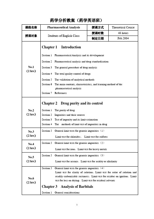
课程名称
授课方式
Theoretical Course
授课对象
3.2 test of related substances in chlorpromazine
3.3 assay
alkalimeteic and non-aqueous alkalimetric、
UV-spetrophotometric、redox titration、colorimetry、
electrochemical and chromatography method
No.6
(2 hrs)
Section 5 General limit tests for generic impurities(4)
Limit test for clarity of solution、Limit test for color of solution and readily carbonizable sustances、Limit test for residue on ignition、Limit test for loss on drying、Limit test for residual solvents
- 1、下载文档前请自行甄别文档内容的完整性,平台不提供额外的编辑、内容补充、找答案等附加服务。
- 2、"仅部分预览"的文档,不可在线预览部分如存在完整性等问题,可反馈申请退款(可完整预览的文档不适用该条件!)。
- 3、如文档侵犯您的权益,请联系客服反馈,我们会尽快为您处理(人工客服工作时间:9:00-18:30)。
44
测试程序的生成
2011-9-5
45
DFT
2011-9-5
46
可测性设计
2011-9-5
47
测试经济学
2011-9-5
48
2000年VLSI电路生产测试成本计算:
如果一个数字IC的测试时间是6秒,则测试费用是27美分,由于 坏芯片不能出售,它们的测试费用只能分摊到好芯片上。假设产品 的良率为65%,则一个好芯片的售价中,测试部分为27/0.65=41.5美 分。
2011-9-5
上海电力学院电子科学与技术系
33
功能测试的类型
测试涉及到测试生成,测试施加和测试分析几个 过程,因此功能测试也按这些过程来分类:
2011-9-5
上海电力学院电子科学与技术系
34
测试方法分类标准 测试实施时间 测试激励源的位置 测试的目的 l l l l l l l l l
测试方法特征 测试实施时电路运行在正常工作条件下 测试施加时与电路运行不同时进行 嵌于电路内部 由外部测试设备提供 设计错误 制造错误 制造缺陷 早期物理失效 物理失效
总结1
本章系统介绍本书的内容和章节结构,并阐述 VLSI测试和可测性设计常用的术语。VLSI测试可分 为三类:一类是验证测试、特征测试或设计诊断, 一类是生产测试,也叫产品测试,第三类是可接受 测试。生产测试又可分为参数测试和功能测试,其 中参数测试的目的是确定制造的产品的逻辑电压值、 电流和延迟等参数是否满足设计参数要求,而功能 测试的目的则是确定制造的产品的逻辑电路/模拟
术语 在线测试 离线测试 自测试 外部测试 设计验证测试 可接受测试 老化 质量保证测试 现场测试 维护测试
被测对象的物理实体
l l l l l l l l l l l l l
IC 板级 系统级 存取 测试过程中生成
器件级测试 板级测试 系统级测试 存储的测试图形测试 算法测试 比较测试 适应测试
激励和理想响应的产生方法
2011-9-5
上海电力学院电子科学与技术系
29
功能测试(封装后)
2011-9-5
上海电力学院电子科学与技术系
30
错误(error)和故障(fault)
2011-9-5
上海电力学院电子科学与技术系
31
建模和模拟
模拟分为逻辑模拟和故障模拟: 逻辑模拟-用计算机模拟计算给定的电路在给定的 输入向量下电路中各引线的稳定逻辑值; 故障模拟-指对给定的输入向量用计算机模拟计算 电路中存在给定故障时各引线的稳定状态,判断所 给向量是否是给定故障的测试码。
9
4,设计挑战
2011-9-5
上海电力学院电子科学与技术系
10
5,Time-to-Market
2011-9-5
上海电力学院电子科学与技术系
11
6,测试设备和测试开发的成本增加
2011-9-5
上海电力学院电子科学与技术系
12
2011-9-5
13
二、测试技术的发展
2011-9-5
上海电力学院电子科学与技术系
2011-9-5
上海电力学院电子科学与技术系
20
特性测试
2011-9-5
上海电力学院电子科学与技术系
21
Shmoo图:VCC-t曲线
2011-9-5
上海电力学院电子科学与技术系
22
生产测试
2011-9-5
上海电力学院电子科学与技术系
23
裸片测试
2011-9-5
上海电力学院电子科学与技术系
24
4
第一章 概述
2011-9-5
5
2011-9-5
上海电力学院电子科学与技术系
6
1,设计与测试紧密相关
2011-9-5
上海电力学院电子科学与技术系
7
2,电路速度、功能和性能不断提高
2011-9-5
上海电力学院电子科学与技术系
8
3,器件复杂程度的提高
2011-9-5
上海电力学院电子科学与技术系
封装后测试
2011-9-5
上海电力学院电子科学与技术系
25
接触测试(封装后)
2011-9-5
上海电力学院电子科学与技术系
26
老化测试(封装后)
2011-9-5
上海电力学院电子科学与技术系
27
老化测试方法
2011-9-5
上海电力学院电子科学与技术系
28
电参数测试(封装后)
有些电路虽然通过了功能测试,但无驱动能力,因此仍是有缺 陷的,此时要进行电参数测试,电参数测试用于确定电路引脚的电 压/电流/延迟时间是否在可接受的范围。
■测试透明度TT=1-T 表示未检测到故障的比率 (T为故障覆盖率)
2011-9-5 51
缺陷等级、测试透明度和良率之间的关系
要保证较低的缺陷等级,就必须降低测试透明度,也就是必须提高故障覆盖率!
2011-9-5 52
DFT对测试经济因素的影响
+表示成本增加,-表示成本减少。
2011-9-5
53
2011-9-5 56
作业
n
P18页 1,5
2011-9-5
57
2011-9-5
上海电力学院电子科学与技术系
3
内容提要:
n n n n n n n
测试与验证的基本术语; 故障模型; 逻辑模拟和故障模拟; 组合电路测试生成方法; 专用可测性设计; 扫描设计,边界扫描设计,内建自测试; IDDQ测试原理; Memory测试; SOC测试。
2011-9-5
上海电力学院电子科学与技术系
激励的施加方法 测试激励施加的快慢
预先确定的顺序 按照当时得到的结果 比正常操作速度慢得多 正常操作速度 所有的输出图形 (部分)特征输出图形 仅IC的I/O IC的I/O或内部I/O
DC(静态)测试,AC测试,高 速测试 压缩测试 引脚测试 探针测试 Bed-of-nails测试 电子显微镜测试/光离子检测/电子 束测试 电路内测试 电路内仿真 自测试/自检查 35 外部测试
测试结果观察方法 测试存取I/O
2011-9-5
测试结果检查者
l l
被测对象本身 外部测试设备
测试施加
2011-9-5
36
在线测试和离线测试
2011-9-5
37
片上测试和片外测试
2011-9-5
38
自动测试设备(ATE)
2011-9-5
39
ATE主要组成部分
2011-9-5
40
ADVANTEST Model T6682 ATE ADVANTEST Model T6682 ATE
2011-9-5
41
Advantest T6682 ATE 的管脚电路
每一个通道都有一个比较器(DUT输出)管脚和常规的驱动器/比较器管脚
2011-9-5
42
LTX FUSION HF ATE-测试SOC LTX FUSION HF ATE-测试SOC
2011-9-5
43
ATPG
2011-9-5
14
可测性设计的发展
2011-9-5
上海电力学院电子科学与技术系
15
三,基本术语
2011-9-5
上海电力学院电子科学与技术系
16
测试(Testing)
2011-9-5
上海电力学院电子科学与技术系
17
测试原理
2011-9-5
18
测试分类
2011-9-5
上海电力学院电子科学与技术系
19
验证测试
2011-9-5
上海电力学院电子科学与技术系
32
测试效率-故障覆盖率 (Fault Coverage,FC)
对于给定的故障模型, FC=测试图形所能检测到该类型故障的数目/电路 中可能存在的所有该故障类型数目*100%
若一测试图形的故障覆盖率为100%,则称该测试 图形为完全测试集; 注意:100%的故障覆盖率并不能保证电路无故障 (因为测试只是对所采用的故障模型所表达的失效 做检验,对其他失效并未检测)
2011-9-5 49
测试经济学
2011-9-5
50
两个概念:良率和缺陷等级
■良率:Y=G/(G+B) G为通过所有测试的芯片数目,B为 未通过部分测试的芯片数目。 ■缺陷等级DL:每百万个芯片中有缺陷的芯 片的个数(DPM:defect per million)
缺陷等级0.1%与1000DPM是同一意思
究的主要内容。
2011-9-5
电路行为是否正确,功能测试方法是本书研
上海电力学院电子科学与技术系
54
总结2
l功能测试按测试生成、测试施加和测试分析
几个过程有多种分类方法,过程一般是先电路 建模,然后测试图形生成,再测试施加,测试 响应分析,最后得出CUT测试通过与否。
2011-9-5
55
总结3
测试必须考虑故障覆盖率、测试时间、 测试必须考虑 测试设备的能力等因素,需要在电路的 建模、验证、测试图形生成和测试施加 诸方面所用的工具、设备和方法研究方 面进行大量的投资,如何在保证产品可 靠性高和上市时间短的情况下才尽可能 降低测试成本,这就是测试经济学要研 究的内容,DFT设计对测试经济因素的 影响也是必须研究的内容。
超大规模集成电路测试
2011-9-5
1
考查方式
ü 平时成绩30% n
包括:考勤,作业等
ü 试卷70%(开卷)
2011-9-5
2
参考书目: 1,《超大规模集成电路测试-数字、存储器和 混合信号系统》 Michael L. Bushnell著 电 子工业出版社 相关网站: 1, 2, 3, 4, 5, 6,