接口软件说明书clock
iclock server使用指南

iClock Server使用指南版本:1.0日期:2008年10月适用机型:iClock300、iClock360、iClock660、iClock2500、iClock2800等机型。
内容介绍本文档主要介绍了iClock Server 系列产品的使用说明,包括软件的安装与卸载,iClock Server的适用。
重要申明首先感谢您选择本系列产品。
在使用前,请您仔细阅读本产品的说明书。
以避免设备受到不必要的损害!本公司提醒您正确使用,将得到良好的使用效果和验证速度。
非经ZKSoftware书面同意,任何单位和个人不得擅自摘抄、复制本手册内容的部分或全部,并不得以任何形式传播。
本手册中描述的产品中,可能包含ZKSoftware及其可能存在的许可人享有版权的软件,除非获得相关权利人的许可,否则,任何人不能以任何形式对前述软件进行复制、分发、修改、摘录、反编译、反汇编、解密、反向工程、出租、转让、分许可以及其他侵权软件版权的行为,但是适用法禁止此类限制的除外。
目录1. iClock Server安装与卸载 (1)1.1 软件的安装 (1)1.2 软件的卸载 (5)2. 登录iClock Server (6)2.1 iClock Server管理 (6)2.2 系统登录及注销 (7)2.3 语言选择 (8)2.4 密码修改 (8)3. iClock Server的使用 (10)3.1 快速使用 (10)3.2 设备管理 (10)3.2.1 设备维护与管理 (10)3.2.2 设备操作日志 (15)3.2.3 实时记录监控 (16)3.3 数据维护 (17)3.3.1 部门管理 (17)3.3.2 人员管理 (19)3.3.3 考勤记录 (24)3.4 系统日志 (27)3.4.1 设备上传数据日志 (27)3.4.2 服务器下发命令日志 (28)3.4.3 管理员操作日志 (30)3.4.4 系统管理员维护 (31)附录 (35)附录1 如何将终端设备连入网络 (35)附录2 常用操作 (37)1. iClock Server安装与卸载1.1 软件的安装1、将安装光盘放入光驱,安装程序会自动运行。
AT32F403A 407时钟配置入门指南说明书

AN0082入门指南AT32F403A/407时钟配置前言本应用入门指南主要介绍两部分内容:1、基于雅特力提供的V2.x.x的板级支持包来进行时钟源码的配置及修改2、如何使用配套的时钟配置工具来进行时钟路径及参数的设定,生成相应的时钟流程代码并使用。
支持型号列表:AT32F403Axx支持型号AT32F407xx目录1简介 (6)2时钟树 (7)3代码配置解析 (9)3.1函数接口 (9)3.2时钟配置流程 (10)3.2.1复位(CRM Reset) (10)3.2.2时钟源配置(Clock Source Configuration) (10)3.2.3PLL配置(PLL Configuration) (11)3.2.4总线分频(Set Bus Frequency Division) (11)3.2.5切换系统时钟(Switch System Clock) (11)3.2.6更新核心频率(Update Core Frequency) (12)3.3时钟配置示例 (13)4时钟工具 (14)4.1环境要求 (14)4.2安装 (14)4.3功能介绍 (14)4.4菜单栏 (15)4.5新建配置项目 (15)4.6配置界面的使用 (16)4.7生成代码 (18)5注意事项 (19)5.1外部时钟源(HEXT)修改 (19)5.2工具使用 (19)6案例系统时钟切换 (20)6.1功能简介 (20)6.2资源准备 (20)6.3软件设计 (20)6.4实验效果 (22)7案例时钟失效检测 (23)7.1功能简介 (23)7.2资源准备 (23)7.3软件设计 (23)7.4实验效果 (24)8文档版本历史 (25)表1. 文档版本历史 (25)图1. 时钟框图 (7)图2. 时钟配置流程图 (10)图3. 启动界面 (14)图4. 配置界面 (15)图5. 菜单栏 (15)图6. MCU选择界面 (16)图7. 配置界面框架 (16)图8. 时钟配置框 (17)1 简介时钟是芯片正确高效运行的基础,正确的时钟配置是芯片能正确运行的必要条件,其重要性不言而喻。
Matrox Solios eCL XCL摄像头接口应用说明书

Photonfocus MV-D1024-28-CL-10 October 5, 2006 Basics about thecameraCamera DescriptionsEffective resolution: 1024 × 1024 × 10-bit @ 27 fps.Camera Link BASE interface (10-bit, single tap).Progressive scan.Internal sync.Internal exposure control.28 MHz pixel clock rate.Mode of operations as per Matrox Imaging (in parentheses as per camera manufacturer)Interface ModeContinuous (Free Running) Pseudo-continuous (Trigger) Asynchronous reset (Trigger)Basics about theinterface modesCamera Interface BriefsMode 1: Continuous1024 × 1024 × 10-bit @ 27 fps.Camera Link BASE interface (10-bit, single tap).Matrox Solios eCL/XCL receiving LVAL, FVAL, PIXEL CLOCK (CLK @28 MHz) and video from camera.DCF used: MVD102428CL10_1024x1024_10bitCon.DCFMode 2: Pseudo-continuous1024 × 1024 × 10-bit.Camera Link BASE interface (10-bit, single tap).Matrox Solios eCL/XCL sending EXPOSURE1 (CC1) signal to camera toinitiate and control the exposure.Matrox Solios eCL/XCL receiving LVAL, FVAL, PIXEL CLOCK (CLK @28 MHz) and video from camera.DCF used: MVD102428CL10_1024x1024_10bitPcon.DCFContinued…Photonfocus MV-D1024-28-CL-10 October 5, 2006 Basics about theCamera Interface Briefs (cont.)interface modesMode 2: Pseudo-continuousMode 3: Asynchronous reset1024 × 1024 × 10-bit.Camera Link BASE interface (10-bit, single tap).Matrox Solios eCL/XCL receiving external trigger signal.Matrox Solios eCL/XCL sending EXPOSURE1 (CC1) signal to camera toinitiate and control the exposure.Matrox Solios eCL/XCL receiving LVAL, FVAL, PIXEL CLOCK (CLK @28 MHz) and video from camera.DCF used: MVD102428CL10_1024x1024_10bitAsync.DCFPhotonfocus MV-D1024-28-CL-10 October 5, 2006 Specifics about theCamera Interface Detailsinterface modesMode 1: ContinuousFrame rate: Matrox Solios eCL/XCL receives the continuous video fromthe camera at 27 frames per second. To increase the frame rate, reduceexposure time in the PhotonFocus PFRemote Camera Configurationutility (PFRemote.EXE).Exposure time: Exposure time is determined by the Exposure TimeField setting in the PFRemote utility. Refer to the camera manual formore information.Camera settings: The camera mode is set to the following setting in thePFRemote utility. Refer to the camera manual for more information.Mode SettingTrigger Free RunningOutput 10-bitConstant Frame Rate uncheckedMode 2: Pseudo-continuousFrame rate: The frame rate is determined by the frequency of theEXPOSURE1 (CC1) signal.Exposure time: The EXPOSURE1 (CC1) signal active duration (high tolow) initiates and controls the camera’s internal exposure time. To modifythe exposure time, in Matrox Intellicam change the Timer 1 value in theDCF or use the MIL MdigControl function. Refer to the MIL on-line Helpfor more information.Camera settings: The camera mode is set to the following setting in thePFRemote utility. Refer to the camera manual for more information.Mode SettingTrigger External TriggerOutput 10-bitSYNC Pulse Active High checkedCombined trigger/exposure checkedConstant Frame Rate uncheckedPhotonfocus MV-D1024-28-CL-10 October 5, 2006 Specifics about theCamera Interface Details (cont.)interface modesMode 3: Asynchronous Reset▪Frame rate: The frame rate is determined by the frequency of theexternal trigger signal. The period between the external trigger signalsmust be larger than the frame readout period and the exposure time.▪Exposure time: Refer to Mode 2: Pseudo-continuous.▪Camera settings: Refer to Mode 2: Pseudo-continuous.Cabling details for theCabling Requirementsinterface modesMode 1 and 2: Continuous and Pseudo-continuous▪Cable and Connection: Standard Camera Link cable.Mode 2: Asynchronous reset▪Cable and Connection: Standard Camera Link.▪External trigger: External trigger should be connected to the OPTOTRIG input of the 9-pin connector (pins 7 and 2) on the Expanded I/Oadapter bracket.EXPANDED I/O BRACKET(9-pin connector) External Trigger SourceOPTOTRIG + 07 ←SIGNAL --OPTOTRIG - 02 ←GROUND --The DCFs mentioned in this application note are also attached (embedded) to this PDF file – use the Adobe Reader’s View File Attachment to access the DCF files. The information furnished by Matrox Electronics System, Ltd. is believed to be accurate and reliable. Please verify all interface connections with camera documentation or manual. Contact your local sales representative or Matrox Sales office or Matrox Imaging Applications at 514-822-6061 for assistance. © Matrox Electronic Systems Ltd, 2006-2011.Matrox Electronic Systems Ltd.1055 St. Regis Blvd.Dorval, Quebec H9P 2T4CanadaTel: (514) 685-2630Fax: (514) 822-6273。
Aurora接口使用说明

在AMC-2C667X平台上使用FPGA的Aurora接口说明声明:本文档仅面向初学者。
1、针对平台用的V6芯片型号新建一个ISE工程,工程中加入Aurora IP核,IP核的设置如下(当然也可以选择其他设置,以下均是针对本测试设置而言)图1主要参数:lanes-通道数,即使用的GTX收发器个数Lane width:aurora 核与用户接口的数据位宽(一般可选2B或者4B)Lane rate:Aurora核的对外通信速率,由于采用8B/10B编码,实际有效速率要乘以0.8。
GT REFCLK:GTX参考时钟频率采用全双工,流水通信模式。
详细请参考Aurora的UG。
好了,最后一页了,这IP核设置够简单吧!!!(一共才两页好伐…),让你选择GTX位置平台上的V6片子一共有6组GTX QUAD,每个QUAD有4个GTX,选择一个GTX与平台的SFP+ F2相连,平台说明书写清楚了,是MGT_113_1,就是它了。
生成了这个核以后,核的文件夹下会多出一堆文件,这就是XILINX给你的一个示例工程-example design.图3接下来就可以仿真啦。
仿真:你可以直接使用它提供的testbench仿真,没问题。
但是有更简单的方法,其实你仿真只是为了看看它的时序,看看你加的东西对不对,因为只要你加对了,仿真一定通过。
那么简单的方法呢?打开modelsim,不要告诉我你没装,或者装了没有关联ISE仿真库,那你得先把这个问题解决了再说。
好了之后,新建一个modelsim工程(file-new…)在你之前那堆文件的/simulation/functional文件夹下,看图说话~下一个界面叫你create new files啥的直接close。
然后你就在modelsim命令窗口轻轻地敲了一行命令:do simulate_mti.do这个simulate_mti.do就是人家已经仿真好的仿真文件,就在那个文件夹里,意思就是我仿好了,你拿去用吧,看看就好,没什么技术含量。
ICS557-01 Datasheet说明书

PCI-EXPRESS CLOCK SOURCEDescriptionThe ICS557-01 is a clock chip designed for use inPCI-Express Cards as a clock source. It provides a pair of differential outputs at 100 MHz in a small 8-pin SOIC package.Using IDT’s patented Phase-Locked Loop (PLL) techniques, the device takes a 25 MHz crystal input and produces HCSL (Host Clock Signal Level) differential outputs at 100 MHz clock frequency. LVDS signal levels can also be supported via an alternative termination scheme.Features•Supports PCI-Express TM HCSL Outputs0.7 V current mode differential pair •Supports LVDS Output Levels•Packaged in 8-pin SOIC•RoHS 5 (green ) or RoHS 6 (green and lead free) compliant packaging•Operating voltage of 3.3 V•Low power consumption•Input frequency of 25 MHz•Short term jitter 100 ps (peak-to-peak)•Output Enable via pin selection•Industrial temperature range availableBlock DiagramPin Assignment Pin DescriptionsPin NumberPinNamePinTypePin Description1OE Input Output Enable signal(H = outputs are enabled, L = outputs are disabled/tristated).Internal pull-up resistor.2X1Input Crystal or clock input. Connect to a 25 MHz crystal or single ended clock. 3X2XO Crystal Connection. Connect to a parallel mode crystal.Leave floating if clock input.4GND Power Connect to ground.5IREF Output A 475Ω precision resistor connected between this pin and groundestablishes the external reference current.6CLK Output HCSL differential complementary clock output.7CLK Output HCSL differential clock output.8VDD Power Connect to +3.3 V.Applications Information External ComponentsA minimum number of external components are required for proper operation.Decoupling CapacitorsDecoupling capacitors of 0.01 μF should be connected between VDD and the ground plane (pin 4) as close to the VDD pin as possible. Do not share ground vias between components. Route power from power source through the capacitor pad and then into IDT pin.CrystalA 25 MHz fundamental mode parallel resonant crystal with C L = 16 pF should be used. This crystal must have less than 300 ppm of error across temperature in order for theICS557-01 to meet PCI Express specifications.Crystal CapacitorsCrystal capacitors are connected from pins X1 to ground and X2 to ground to optimize the accuracy of the output frequency.C L= Crystal’s load capacitance in pFCrystal Capacitors (pF) = (C L- 8) * 2For example, for a crystal with a 16 pF load cap, each external crystal cap would be 16 pF. (16-8)*2=16.Current Source (Iref) Reference Resistor - R RIf board target trace impedance (Z) is 50Ω, then R R = 475Ω(1%), providing IREF of 2.32 mA. The output current (I OH) is equal to 6*IREF.Output TerminationThe PCI-Express differential clock outputs of the ICS557-01 are open source drivers and require an external series resistor and a resistor to ground. These resistor values and their allowable locations are shown in detail in thePCI-Express Layout Guidelines section.The ICS557-01can also be configured for LVDS compatible voltage levels. See the LVDS Compatible Layout Guidelines sectionGeneral PCB Layout RecommendationsFor optimum device performance and lowest output phase noise, the following guidelines should be observed.1. Each 0.01µF decoupling capacitor should be mounted on the component side of the board as close to the VDD pin as possible.2. No vias should be used between decoupling capacitor and VDD pin.3. The PCB trace to VDD pin should be kept as short as possible, as should the PCB trace to the ground via. Distance of the ferrite bead and bulk decoupling from the device is less critical.4. An optimum layout is one with all components on the same side of the board, minimizing vias through other signal layers (any ferrite beads and bulk decoupling capacitors can be mounted on the back). Other signal traces should be routed away from the ICS557-01.This includes signal traces just underneath the device, or on layers adjacent to the ground plane layer used by the device.PCI-Express Layout GuidelinesFigure 1: PCI-Express Device RoutingTypical PCI-Express (HCSL) WaveformLVDS Compatible Layout GuidelinesFigure: LVDS Device RoutingTypical LVDS WaveformAbsolute Maximum RatingsStresses above the ratings listed below can cause permanent damage to the ICS557-01. These ratings are stress ratings only. Functional operation of the device at these or any other conditions above those indicated in the operational sections of the specifications is not implied. Exposure to absolute maximum rating conditions for extended periods can affect product reliability. Electrical parameters are guaranteed only over the recommended operating temperature range.DC Electrical CharacteristicsUnless stated otherwise, VDD = 3.3 V ±5%, Ambient Temperature -40 to +85°C1 Single edge is monotonic when transitioning through region.2 Inputs with pull-ups/-downs are not included.ItemRatingSupply Voltage, VDD, VDDA 5.5 VAll Inputs and Outputs-0.5 V to VDD+0.5 V Ambient Operating Temperature (commercial)0 to +70°C Ambient Operating Temperature (industrial)-40 to +85°C Storage Temperature -65 to +150°C Junction Temperature 125°C Soldering Temperature 260°CESD Protection (Input)2000 V min. (HBM)ParameterSymbolConditions Min.Typ.Max.UnitsSupply Voltage V 3.135 3.465Input High Voltage 1V IH 2.0VDD +0.3V Input Low Voltage 1V IL VSS-0.30.8V Input Leakage Current 2I IL 0 < Vin < VDD-55μA Operating Supply Current I DD With 50Ω and 2 pF load 55mA I DDOE OE =Low35mA Input Capacitance C IN Input pin capacitance 7pF Output Capacitance C OUT Output pin capacitance 6pF Pin Inductance L PIN 5nH Output Resistance Rout CLK outputs 3.0k ΩPull-up ResistorR PUPOE60k ΩAC Electrical Characteristics - CLK/CLKUnless stated otherwise, VDD=3.3 V ±5%, Ambient Temperature -40 to +85°C1 Test setup is R L =50 ohms with2 pF , R R = 475Ω (1%).2 Measurement taken from a single-ended waveform.3 Measurement taken from a differential waveform.4Measured at the crossing point where instantaneous voltages of both CLKOUT and CLKOUT are equal.5 CLKOUT pins are tri-stated when OE is low asserted. CLKOUT is driven differential when OE is high.Thermal Characteristics (8-pin SOIC)ParameterSymbolConditions Min.Typ.Max.UnitsInput Frequency 25MHz Output Frequency 100MHzOutput High Voltage 1,2V OH 660700850mV Output Low Voltage 1,2V OL-150027mV Crossing Point Voltage 1,2Absolute250350550mV Crossing Point Voltage 1,2,4Variation over all edges140mV Jitter, Cycle-to-Cycle 1,380ps Rise Time 1,2t OR From 0.175 V to 0.525 V 175332700ps Fall Time 1,2t OFFrom 0.525 V to 0.175 V175344700ps Rise/Fall Time Variation 1,2125ps Duty Cycle 1,34555%Output Enable Time 5All outputs 30µs Output Disable Time 5All outputs30µs Stabilization Time t STABLEFrom power-up VDD=3.3 V3.0ms Spread Change Timet SPREAD Settling period after spread change3.0msParameterSymbolConditionsMin.Typ.Max.UnitsThermal Resistance Junction to AmbientθJA Still air150°C/W θJA 1 m/s air flow 140°C/W θJA 3 m/s air flow120°C/W Thermal Resistance Junction to CaseθJC40°C/WMarking Diagram (ICS557M-01LF) Marking Diagram (ICS557MI-01LF)Notes:1. ###### is the lot code.2. YYWW is the last two digits of the year, and the week number that the part was assembled.3. “L ” designates Pb (lead) free packaging.4. “I” denotes industrial temperature.5. Bottom marking: (orgin). Origin = country of origin if not USA.Package Outline and Package Dimensions (8-pin SOIC, 150 Mil. Narrow Body) Package dimensions are kept current with JEDEC Publication No. 95Ordering InformationPart / Order Number Marking Shipping Packaging Package Temperature 557M-01LF See Page 8Tubes8-pin SOIC0 to +70° C557M-01LFT Tape and Reel8-pin SOIC0 to +70° C557MI-01LF Tubes8-pin SOIC-40 to +85° C557MI-01LFT Tape and Reel8-pin SOIC-40 to +85° C"LF" suffix to the part number are the Pb-Free configuration and are RoHS compliant.While the information presented herein has been checked for both accuracy and reliability, Integrated Device Technology (IDT) assumes no responsibility for either its use or for the infringement of any patents or other rights of third parties, which would result from its use. No other circuits, patents, or licenses are implied. This product is intended for use in normal commercial applications. Any other applications such as those requiring extended temperature range, high reliability, or other extraordinary environmental requirements are not recommended without additional processing by IDT. IDT reserves the right to change any circuitry or specifications without notice. IDT does not authorize or warrant any IDT product for use in life support devices or critical medical instruments.Corporate HeadquartersIntegrated Device Technology, For Sales800-345-7015408-284-8200Fax: 408-284-2775For Tech Support/go/clockhelpInnovate with IDT and accelerate your future networks. Contact:www.IDT .com。
RME MADIface XT音频接口用户手册说明书
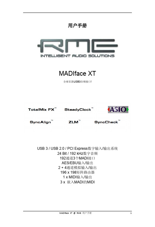
用户手册MADIface XT全球首款USB3音频接口!USB 3 / USB 2.0 / PCI Express数字输入/输出系统24 Bit / 192 kHz数字音频192通道3个MADI接口AES/EBU输入/输出2 + 4通道模拟输入/输出196 x 198矩阵路由器1 x MIDI输入/输出3 x 嵌入MADI的MIDI重要的安全说明 (6)概述 (7)1. 简介 (8)2. 包装清单 (8)3. 系统要求 (8)4. 简介及主要特点 (8)5. 首次使用——快速上手 (9)5.1 接口、控制与显示 (9)5.2 快速上手 (10)安装与操作——Windows (11)6. 硬件、驱动和固件安装 (12)6.1 驱动安装 (12)6.2 驱动卸载 (12)6.3 固件升级 (12)7. 设置MADIface XT (13)7.1 Settings(设置)对话框—主标签 (13)7.2 WDM Devices(WDM设备)选项 (16)7.3 Global选项卡(PCI Express模式) (18)7.4 Pitch(仅E-PCIe支持) (19)7.5 时钟模式–同步 (20)8. 操作和使用 (21)8.1 播放 (21)8.2 播放DVD (AC-3/DTS) (22)8.3 多客户端操作 (23)8.4 数字录音 (23)8.5 模拟录音 (23)9. ASIO下的操作 (24)9.1 概述 (24)9.2 已知问题 (24)10. 使用多个MADIface XT (25)11. DIGICheck Windows (26)12. 热线–故障处理 (27)安装与操作——Mac OS X (28)13.驱动和Flash更新 (29)13.1 驱动安装 (29)13.2 驱动卸载 (29)13.3 固件升级 (30)14. 设置MADIface XT (31)14.1 Settings(设置)对话框 (31)14.2 时钟模式–同步 (33)15. Mac OS X FAQ (34)15.1 MIDI不工作 (34)15.2 修复磁盘权限 (34)15.3 支持的采样率 (34)15.4 各种信息 (34)16. 使用多个MADIface XT (35)17. DIGICheck Mac (35)18. 热线–故障处理 (36)19. 前面板操作 (38)19.1 概述 (38)19.2 Encoders(旋钮) (38)19.3 Menu(菜单)键— MIC/GAIN(话筒/增益)和METERS(电平表) (39)19.4 Channel(通道)菜单 (39)19.5 Setup(设置)菜单 (41)19.5.1 Options(选项)菜单 (41)19.5.2 Setups(设置)菜单 (42)19.6 Clock(时钟) (43)输入和输出 (44)20. 模拟输入/输出 (45)20.1 Mic / Line In (话筒/线路输入,XLR/TRS) (45)20.2 幻象供电 (45)20.3 AutoSet(自动设置) (45)20.4 Balanced Line Outputs(平衡线路输出) (46)20.5 Line – Headphones(线路-耳机) (46)21. 数字输入和输出 (47)21.1 MADI输入/输出 (47)21.2 AES/EBU (47)21.3 MIDI (47)21.4 D-sub针脚 (48)22. 字时钟 (49)22.1 字时钟输入和输出 (49)22.2 技术描述和使用 (50)22.3 布线和终止 (51)独立工作模式 (52)23. 操作和使用 (53)23.1 概述 (53)23.2 在设备上设置 (53)24. 实例 (54)24.1 2/4通道AD/DA转换器 (54)24.2 2通道话筒放大器 (54)24.3 194通道监听混音器 (54)24.4 模拟和数字插入器 (54)24.5 带有监听的3端口MADI路由器 (54)TotalMix FX (55)25. TotalMix:路由和监听 (56)25.1 概述 (56)25.2 用户界面 (58)25.3 通道 (59)25.3.1 设置 (61)25.3.2 均衡器 (62)25.3.3 动态 (64)25.4 控制室栏 (65)25.5 控制条 (66)25.5.1 视图选项 (67)25.5.2 快照-组 (68)25.5.3 通道布局-布局预设 (68)25.5.4 滚动位置标记 (70)25.7 首选项 (74)25.7.1 为当前所有用户保存(Windows) (75)25.8 设置 (76)25.8.1 混音器页面 (76)25.8.2 MIDI 页面 (77)25.8.3 OSC页面 (78)25.8.4 辅助设备 (79)25.9 热键与使用 (80)25.10 菜单选项 (80)25.11 菜单窗口 (82)26. 矩阵 (82)26.1 概述 (82)26.2 矩阵视图元素 (82)26.3 操作 (82)27. 操作技巧 (83)27.1 ASIO直接监听(Windows) (83)27.2 复制子混音 (83)27.3 复制一个输出信号(镜像) (83)27.4 删除子混音 (83)27.5 任意复制和粘贴 (84)27.6 录制子混音–回路 (84)27.7 MS 处理 (85)28. MIDI 远程控制 (86)28.1 概述 (86)28.2 规划 (86)28.3 设置 (87)28.4 操作 (87)28.5 MIDI控制 (88)28.6 回路检测 (89)28.7 OSC (89)技术参考资料 (90)29. 技术指标 (91)29.1 模拟 (91)29.2 数字输入 (92)29.3 数字输出 (92)29.4 数字 (93)29.5 MIDI (93)29.6 通用 (93)30. 技术背景 (94)30.1 MADI基础 (94)30.2 锁定(Lock)与SyncCheck(同步检查) (95)30.3 延时(Latency)与监听(Monitoring) (95)30.4 USB音频 (97)30.5 External PCI Express (98)30.6 DS –双倍速 (99)30.7 QS –四倍速 (99)30.8 SteadyClock(稳定时钟) (100)30.9 WDM的注意事项 (101)30.10 术语 (102)其他 (103)31. 配件 (104)32. 产品保证 (104)33. 附录 (105)34. 符合性声明 (105)重要的安全说明注意! 不要打开底盘,以防触电。
时钟(AnalogClock和DigitalClock)的功能与用法

时钟(AnalogClock和DigitalClock)的功能与⽤法时钟UI组件是两个⾮常简单的组件,DigitalClock本⾝就继承了TextView——也就是说它本⾝就是⽂本框,只是它⾥⾯显⽰的内容总是当前时间。
与TextView不同的是为DigitalClock设置android:text属性没什么作⽤。
AnalogClock则继承了View组件,他重写了View的OnDraw⽅法,它会在View上绘制模拟时钟。
表2.16显⽰了AnalogClock所⽀持的XML属性的说明。
表2.16 AnalogClock⽀持的XML属性的说明XML属性说明android:dial设置该模拟时钟的表盘使⽤的图⽚android:hand_hour设置该模拟时钟的时针表盘使⽤的图⽚android:hand_minute设置该模拟时钟的分针使⽤的图⽚DigitalClock和AnalogClock都会显⽰当前时间。
不同的是,DigitalClock显⽰数字时钟,可以显⽰当前的秒数;AnalogClock显⽰模拟时钟,不会显⽰当前秒数。
通过下⾯的实例来⽰范AnalogClock和DigitalClock的⽤法。
实例:⼿机⾥的“劳⼒⼠”由于我们可以通过图⽚定制AnalogClock模拟指针的表盘、时针、分针,因此只要使⽤合适的图⽚,就可以对AnalogClock进⾏任意定制。
下⾯的实例将会使⽤“劳⼒⼠”图⽚来定义模拟时钟,从⽽开发⼿机⾥⾯的“劳⼒⼠”。
下⾯是本实例的布局⽂件。
<LinearLayout xmlns:android="/apk/res/android"android:orientation="vertical"android:layout_width="fill_parent"android:layout_height="fill_parent"android:gravity="center_horizontal"><!-- 定义模拟时钟 --><AnalogClock android:layout_width="wrap_content"android:layout_height="wrap_content"/><!-- 定义数字时钟 --><DigitalClockandroid:layout_width="wrap_content"android:layout_height="wrap_content"android:textSize="14pt"android:textColor="#f0f"android:drawableRight="@drawable/ic_launcher"/><!-- 定义模拟时钟,并使⽤⾃定义表盘,时针图⽚ --><AnalogClock android:layout_width="wrap_content"android:layout_height="wrap_content"android:dial="@drawable/watch"android:hand_minute="@drawable/hand" /></LinearLayout>使⽤Activity显⽰上⾯的界⾯布局,将会看到2.27所⽰的界⾯。
simulink clock模块用法

simulink clock模块用法
SimulinkClock模块是一种用于模拟时钟信号的模块,可以用于控制模型中的事件发生时间和时序。
在使用Simulink Clock模块时,可以设置时钟的周期、启动时间、停止时间、时钟类型等参数。
具体用法如下:
1. 打开Simulink Library Browser,选择Sources库,找到Clock 模块,将其拖放到工作区中。
2. 双击Clock模块,弹出Clock参数对话框。
在该对话框中,可以设置时钟的周期、启动时间、停止时间、时钟类型等参数。
3. 设置时钟周期:在Clock参数对话框中,将Period选项设置为所需的周期,单位为秒。
4. 设置启动时间和停止时间:在Clock参数对话框中,将Start time选项设置为所需的启动时间,将Stop time选项设置为所需的停止时间,单位均为秒。
5. 设置时钟类型:在Clock参数对话框中,将Clock type选项设置为所需的时钟类型,例如Discrete、Continuous、Fixed-step 等。
6. 将Clock模块输出连接到其他模块的输入端口:在模型中使用Clock模块时,将其输出连接到其他模块的输入端口。
通过以上步骤,就可以使用Simulink Clock模块来模拟时钟信号,控制模型中的事件发生时间和时序。
- 1 -。
- 1、下载文档前请自行甄别文档内容的完整性,平台不提供额外的编辑、内容补充、找答案等附加服务。
- 2、"仅部分预览"的文档,不可在线预览部分如存在完整性等问题,可反馈申请退款(可完整预览的文档不适用该条件!)。
- 3、如文档侵犯您的权益,请联系客服反馈,我们会尽快为您处理(人工客服工作时间:9:00-18:30)。
目录第一章卡钟管理 (2)1. 添加设备 (2)2. 基本操作 (4)2.1、读取数据 (4)2.2、设置管理卡 (5)2.3、更改机号 (5)2.4 工作模式 (5)2.5、校正时间 (7)2.6、设置密码 (8)2.7、修改波特率 (8)2.8、实时监控 (8)2.9、取回时间 (9)2.10、机具状态 (10)2.11、清除数据 (10)2.12 在线检测 (11)3. 参数设置 (11)3.1 刷卡间隔 (11)4.显示控制 (12)4.1 自定义显示 (12)5.时段设置 (13)5.1 考勤时段设置 (13)5.2打铃时段设置 (14)6. 考勤名单管理 (14)7. 分组设置和IC卡操作 (16)第二章文件设置 (19)1. 定时间采集 (19)2. 定义文件格式 (19)第三章系统设置 (20)1. 界面风格设置 (20)2. 数据库接口定义 (20)第四章设机器密码 (21)第五章升级机具 (23)第六章IC卡加密 (26)第一章卡钟管理1. 添加设备在进入考勤管理界面后,让我们先看看考勤界面的设备列表中有哪些功能,在列表中右键就会弹出这些功能,都是对机具进行设置的,添加,修改,删除这些也就不用我不介绍了。
主要是看看下面的几项:1、读取参数,就是对机具原有的,或者是已经设置好的参数进行读取,主要读的参数是刷卡间隔时间,重复间隔,外接设备的点亮时间等。
2、下载字库,这项功能是为了适合所有客户的需求,专门下载繁体字库的。
我们的软件也同样配套有繁体版本。
3、参数初始化,是对机具的所有参数进行出厂值的恢复。
4、机具初始化是把机具进行所有设置的初始化,包括存储的纪录,名单等都会被变成“零”。
5、升级模式,是对机具进行升级的程序,可以点击升级模式进入升级界面对机具进行升级处理。
并且我们的软件还支持在线升级,所以在任何时候都可以对机具进行最新版本的轻松升级处理。
在这个操作的流程中要注意很多问题。
1、首先你要将考勤机连接到电脑上,就要选择用什么样的通讯方式?我们的软件提供了三种通讯方式:RS-232,RS-485,TCP/IP。
A、RS-232的特点是:安装布线简单,费用小,适合人少小型的办公区等工程使用,缺点:通讯距离很短,通讯速度满,一般在20M,不适合大型的工程安装。
B、RS-485的特点是:通讯距离远,适合人多流量大,门多的大型工程安装使用,通讯距离在1200M,通讯容量标准是30台机具同时通讯,最大可以连接400台机具,统一管理方便,培训简单,。
缺点:安装布线维护的难度大,所需费用较高。
C、TCP/IP除了集中以上所有的优点外,还有速度更快,安装更简单,联网数量更大,可以跨地域联网考勤,但是价格高,需要网络支持,同时要求使用这要懂基本的网络知识才行。
2、机号的填写,在填写的机号的时候一定要和考勤机上所显示的机号一致。
3、序列号的填写,每一个机具的后盖都有一个唯一的机具号码,所以在填写的时候必须按照后盖上的机具号填写。
4、机型的选择。
这是一个非常关键的选择,因为我们的考勤机机具分为三种系列:CO380,CT380,CU380。
其中CO380又分为:CO380C和CO380D两种机型,他们的区别就是所使用的卡的类型不一样,前者用的是IC卡,而后者用的是ID卡。
同样CT380也分IC和ID的两种卡类型。
CU就是U盘考勤机,可以不用和电脑连接,直接用U盘来存储考勤数据。
5、COM端口,什么是COM端口呢?就是通讯线和电脑连接的那个接口,就称为COM端口。
一般台式电脑有2~3个COM端口,从上到下依次是COM1,COM2…..。
你的通讯线接的是哪个端口就选择哪个端口。
6、波特率,就是通讯的速率。
RS-232的通讯速率在9600bps~~115200bps。
7、TCP/IP,因为在选择机具的时候,如果选择的机具是CT380系列的,我们就需要在这一行输入我们本机的IP地址这样才能使机具和电脑进行通讯。
如图以上每一个设置都会影响到设备和电脑是否能进行正常通讯,所以在选择的时候一定要保证设置正确。
如果设备和电脑进行正常通讯,那么检测设备在线的话。
就会出现绿色连接。
以下就是考勤管理的标准界面。
2. 基本操作在考勤设备的基本设置中包括了几个部分:读取数据,设置管理卡,更改机号,工作模式,校正时间,设置密码,修改波特率,实时监控,取回时间,机具状态,清楚数据,在线检测。
下面就一一介绍他们的功能以及注意事项。
2.1、读取数据就是在打卡考勤完了之后,对机具里面存储的数据读到电脑上来,进行部门和个人的上班考勤。
读取数据的方式是分页读取。
2.2、设置管理卡2.3、更改机号就是对现在在线的机具进行机号的更改。
因为初始化了的机具都是默认的1号机具。
所以在添加很多台机具的时候就需要更改机号才能添加。
2.4 工作模式2.4.1、应用模式应用模式是设备在读卡,纪录存储/名单检查,打卡响铃,外接设备的操作。
在应用模式中有功能用途类型,我们在选择用途类型的时候要知道我们的设备是做什么用的,是做为读卡器来发卡,还是做为考勤机来考勤用的。
实时监控模式的选择是选择打卡的时候是以什么方式来报告刷卡的结果。
选择刷卡处理结果报告查询就是在刷卡的时候显示是不是正常考勤,并且显示卡号和刷卡时间,机具号。
卡片的解析类型就是你要选择你用的卡片是什么类型的卡,如IC,ID的读的方式。
2.4.2 纪录存储/名单检查在工作模式中还有一项是很重要的就是纪录存储/名单检查,在这个界面中两个模块进行不同的设置,就会出现不同的结果,纪录存储模式中,可以同时纪录正常刷卡纪录和非法刷卡纪录,非允许时段刷卡操作时存储纪录等。
如果在前面打勾的话就选中,就会对所有的刷卡信息进行纪录。
在刷卡检查方式中,如果在前面打勾就会对用户的授权信息进行检查,如果不在授权范围内的话就不允许刷卡或者是无效卡。
2.4.3 操作响铃提示所以以上设置如果设置不同,就会出现不能打卡或者其他原因。
下面介绍操作响铃提示,就是你选择在什么情况下刷卡会响铃。
如:正常刷卡响铃,非法刷卡响铃,重复刷卡响铃等。
2.4.4外接设备设定外接设备设定,是除了考勤设备外还接有其他设备,如报警灯等就需要在这个界面中来设置。
如图:2.5、校正时间是对设备上显示的时间和电脑上的时间进行同步。
如果设备和电脑没有正常连接,就会出现校正时间失败,如图:2.6、设置密码就是对现在在线的设备进行密码的设置。
2.7、修改波特率前面已经提到我们的机具有几种波特率,前面已经很详细了,所以在这里就不多讲,就是对机具修改不同波特率进行通讯。
2.8、实时监控就是随时可以看见刷卡的信息,电脑和考勤机上的数据是同步的,监视的类型分为“刷卡结果处理报告查询”就是显示出刷卡的是否为正常刷卡,同时显示刷卡卡号,时间,机号,标识。
“监视刷卡卡号查询报告/允许PC端发送信息”就是只对卡号进行监视,确认卡是否是有效卡,如果是刷卡成功就会自动发送消息。
2.9、取回时间也是对通讯同步的检测,并且对机具的时间取出来进行显示。
2.10、机具状态是显示当前机具的存储状态。
可以看到石碑的序列号,允许存储的最大纪录数和已存储的打卡纪录数,允许存储的最大名单其中白名单数和黑名单数,门禁的通行名单数等。
这样在这里面就可以对机具的当前状态一目了然了。
2.11、清除数据就是只对机具上的打卡纪录进行清除,一般在打卡打满了已经采集完数据之后才进行数据的清除,如果在未采集数据就将数据清除是不能再恢复的,希望在操作时慎用这个功能。
2.12 在线检测是对设备是否与电脑正常连接,而进行的检测,可以检测到那些设备在线,如果检测成功就会出现100%。
并且连接显示绿色。
否则就会显示黄色。
3. 参数设置3.1 刷卡间隔刷卡间隔分为自由间隔和重复间隔。
自由间隔是指两次的刷卡时间之间的长短,我们可以设置的范围是:0~255,每个单位表示0.25秒。
我们通常都设置为“0”意思是不需要间隔,卡任何时候只要放在机具上就可以读取卡。
此外还有重复间隔,是为什么防止在一段时间,连续刷几次卡!外接设备的点亮时间,这个根据外接的设备来确定时间,一般是机具默认。
4.显示控制4.1 自定义显示显示控制分为自定义显示:就是可以根据客户的需要来显示开机信息,产品的型号,产品名称等都是可以由自己来设定。
如果空白就显示本公司的信息。
显示控制参数,可以对刷卡信息在机具上显示保留时间的长短设置,我们一般设置为3秒,卡号长度一般设置为8~10位。
在显示参数中,我们还增加了“高级设置”,可以选择使用的语言,时间显示的格式,日期,图标等;刷卡显示信息的控制,在进入页面后按照自己的需要设置就可以了。
设置简单易看懂,就不用一一介绍了。
5.时段设置5.1 考勤时段设置时段设置分为:考勤时段设置和打铃时段设置。
选择考勤时段,然后进行添加的,考勤时段的设置是设置在哪段时间范围内打卡才是有效的或者是才能打卡的,不在时段内是不能打卡的。
5.2打铃时段设置打铃时段的设置:比如设置在星期一到星期六下午17:30设置为下班打铃时段,持续时间10秒钟,就会设置的时间17:30开始打铃,提示下班时间。
6. 考勤名单管理考勤名单管理:是将所有考勤人员信息写入设备。
可以进行一个一个的添加名单,直接输入卡号确定,就会在列表中小时出现,然后再将名单写入到设备中,这样这个人的信息就存储在机具中了。
如图:为了节省时间和导入的数量,我们还增加了批量导入的方式。
直接先用文档建好名单,然后直接入到设备列表中去。
有人肯定要问了,那我怎么知道要什么样的格式才能导入进去呢?的确如果格式不对的话就不能导入成功,所以我们在建名单前,先用上面的添加名单,添加一个卡号和姓名到列表中去,然后再用软件上的导出功能将刚刚添加进去的名单导出来存储在指定的位置,这样不就有了格式了吗?我们可以进行白名单和黑名单的写入,在这里就只介绍白名单的导入,黑名单和白名单的导入操作都是一样的。
导入名单到列表中后不代表机具中有已经存在名单了,所以大家不要在这个时候就认为工作做完了,因为我们只是将名单导进列表,并没有写入设备,所以接来我们要将名单写入设备中去,如图:此外还增加了查询功能,就是查询某个员工的信息是否已经写入到设备中去了,输入卡号查询是否存在。
如果设备中已经有名单了,就会出现以下的提示,如图:“0001卡号机存在卡号=01,姓名=张三的白名单”。
7. 分组设置和IC卡操作IC卡存储区域:IC卡分为:16个存储扇区,密码存储在0扇区,其他扇区就可以对IC 卡的信息进行存储,这样选择扇区存储的好处在于一张卡可以同时在几中不同的机具上使用。
而每个机具又只会识别本机具存储进去的扇区信息,并且他们之间不会互相干扰,或者读取错误。
还可以对IC卡进行设置密码。
发卡方式,在这个接口软件中,我们软件也同样提供了两种发卡方式:单张和批量发卡。