材料物理化学 第三篇习题
鲁科版 高中化学 选修三 第3章 物质的聚集状态与物质性质 寒假复习题含答案
绝密★启用前鲁科版高中化学选修三第3章物质的聚集状态与物质性质寒假复习题本试卷分第Ⅰ卷和第Ⅱ卷两部分,共100分,考试时间90分钟。
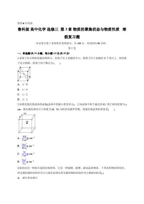
第Ⅰ卷一、单选题(共10小题,每小题4.0分,共40分)1.某离子化合物的晶胞如图所示。
阳离子位于晶胞的中心,阴离子位于晶胞的8个顶点上,则该离子化合物阴、阳离子的个数比为 ()A. 1∶8B. 1∶4C. 1∶2D. 1∶12.如图是氯化铯晶体的晶胞(晶体中的最小重复单元),已知晶体中两个最近的Cs+离子核间距离为a cm,氯化铯的相对分子质量为M,N A为阿伏加德罗常数,则氯化铯晶体的密度是()A.g·cm-3B.g·cm-3C.g·cm-3D.g·cm-33.氮化硅是一种新合成的结构材料,它是一种超硬、耐磨、耐高温的物质。
下列各组物质熔化时,所克服的微粒间的作用力与氮化硅熔化所克服的微粒间的作用力都相同的是( )A.硝石和金刚石B.晶体硅和水晶C.冰和干冰D.萘和蒽4.我国科学家研制出一种催化剂,能在室温下高效催化空气中甲醛的氧化,其反应如下:HCHO+O2CO2+H2O。
下列有关说法正确的是()A.该反应为吸热反应B. CO2分子晶体中的化学键为非极性键,C. HCHO分子中既含σ键又含π键D.每生成1.8 g H2O消耗2.24 L O25.为了确定SbCl3、SbCl5是否为离子化合物,以下分析正确的是()A.常温下,SbCl3、SbCl5均为液体,说明SbCl3和SbCl5都是离子化合物B. SbCl3、SbCl5的熔点依次为73.5 ℃、2.8 ℃。
说明SbCl3、SbCl5都不是离子化合物C.SbCl3、SbCl5溶液中,滴入酸化的AgNO3溶液,产生白色沉淀。
说明:SbCl3、SbCl5都是离子化合物D. SbCl3、SbCl5的水溶液都可以导电。
说明:SbCl3、SbCl5都是离子化合物6.钛酸钡的热稳定性好,介电常数高,在小型变压器、话筒和扩音器中都有应用.钛酸钡晶体的晶胞结构示意图如图所示,它的化学式是()A. BaTi8O12B. BaTi4O6C. BaTi2O4D. BaTiO37.四氯化硅的分子结构与四氯化碳类似,对其作出如下推测:①四氯化硅晶体是分子晶体②常温常压下四氯化硅是液体③四氯化硅分子是由极性键形成的分子④四氯化硅熔点高于四氯化碳。
第五版物理化学第三章习题答案-图文

第五版物理化学第三章习题答案-图文以下是为大家整理的第五版物理化学第三章习题答案-图文的相关范文,本文关键词为第五,物理化学,第三章,习题,答案,图文,第三章,热力学,第,您可以从右上方搜索框检索更多相关文章,如果您觉得有用,请继续关注我们并推荐给您的好友,您可以在综合文库中查看更多范文。
第三章热力学第二定律3.1卡诺热机在(1)热机效率;(2)当向环境作功。
解:卡诺热机的效率为时,系统从高温热源吸收的热及向低温热源放出的热的高温热源和的低温热源间工作。
求根据定义3.2卡诺热机在(1)热机效率;(2)当从高温热源吸热解:(1)由卡诺循环的热机效率得出时,系统对环境作的功的高温热源和的低温热源间工作,求:及向低温热源放出的热(2)3.3卡诺热机在(1)热机效率;(2)当向低温热源放热解:(1)时,系统从高温热源吸热及对环境所作的功。
的高温热源和的低温热源间工作,求1(2)3.4试说明:在高温热源和低温热源间工作的不可逆热机与卡诺机联合操作时,若令卡诺热机得到的功wr等于不可逆热机作出的功-w。
假设不可逆热机的热机效率大于卡诺热机效率证:(反证法)设ηir>ηr不可逆热机从高温热源吸热则,向低温热源放热,对环境作功,其结果必然是有热量从低温热源流向高温热源,而违反势热力学第二定律的克劳修斯说法。
逆向卡诺热机从环境得功则从低温热源吸热向高温热源放热若使逆向卡诺热机向高温热源放出的热不可逆热机从高温热源吸收的热相等,即总的结果是:得自单一低温热源的热,变成了环境作功,违背了热力学第二定律的开尔文说法,同样也就违背了克劳修斯说法。
23.5高温热源温度低温热源,求此过程。
,低温热源温度,今有120KJ的热直接从高温热源传给解:将热源看作无限大,因此,传热过程对热源来说是可逆过程3.6不同的热机中作于情况下,当热机从高温热源吸热(1)可逆热机效率(2)不可逆热机效率(3)不可逆热机效率解:设热机向低温热源放热。
物理化学习题解

物理化学习题解 -CAL-FENGHAI-(2020YEAR-YICAI)_JINGBIAN第三章 化学反应系统热力学 练 习 题3-4 在291~333K 温度范围内,下述各物质的C p,m /(JK -1mol -1)分别为 CH 4(g): 35.715; O 2(g): 29.36; CO 2(g): 37.13; H 2O(l): 75.30;在298.2K 时,反应 CH 4 (g) + 2O 2(g)==CO 2(g) + 2H 2O(l) 的恒压反应热效应为 -890.34kJmol -1。
.求 333K 时该反应的恒容反应热效应为多少解:(1) 求333K 时恒压反应热效应: ΔH (333K) =ΔH (298.2K)+⎰∆333298d TC p = -887.0 kJ mol -1(2) 求恒容反应热效应: ΔU (333K) =ΔH (333K) - ∑BB )(RT g ν= -881.6kJmol -13-5 由以下数据计算2,2,3,3四甲基丁烷的标准生成热。
已知:Om f H ∆[H(g)]=217.94 kJ mol -1,Omf H ∆[C(g)]=718.38 kJmol -1,εC-C =344 kJmol -1,εC-H = 414 kJmol -1。
解:Om f H ∆[CH 3C(CH 3)2 C(CH 3)2 CH 3 (g)]=18Om f H ∆[H(g)]+8Om f H ∆[C(g)]-7εC-C -18εC-H = -190 kJ mol -13-6 已知计算25解:CH 3OH(l)→CH 3OH(g) ,Om r G ∆=[-200.7-(-238.7)]-T [239.7-127.0]×10-3= 4.4 kJ mol -1 O m r G ∆=O ln K RT -, O K =p */O p , p *=1.7×10⁴Pa3-8 已知反应C(石墨)+H 2O(g)→CO(g)+H 2(g) 的 Om r H ∆(298.15 K) =133 kJ mol -1,计算该反应在125℃时的 Om r H ∆(398.15K)。
物理化学3答案资料
物理化学试卷班级 姓名 分数一、选择题 ( 共 8题 15分 ) 1. 2 分 (5553) 55531-1 级对峙反应 12AB k k 由纯 A 开始反应,当进行到 A 和 B 浓度相等的时间为: (正、逆向反应速率常数分别为 k 1 ,k 2) ( ) (A) t = ln12k k (B) t =11221ln kk k k -(C) t =1121212ln k k k k k +-(D) 112121ln k t k k k k =+-2. 2 分 (9109) 9108吉布斯自由能判据可以写作: ( ) (A )(d G )T, p, W =0 ≤0 (B )(d G )f,,0T p W=≤0(C )(d G )T, p, W =0 ≥0 (D )(d G )f,,0T p W=≥03. 2 分 (2184) 2184在310 K,纯H 2O(l)的蒸气压为6.275 kPa,现有1 mol 不挥发物质B(s)溶于4 mol H 2O(l)形成溶液,若溶液中水的活度为0.41(以纯水为标准态),则溶解过程中1 mol H 2O(l)的Gibbs 自由能变化为:( ) (A) -557 J ⋅mol -1 (B) -2298 J ⋅mol -1 (C) -4148 J ⋅mol -1 (D) 4148 J ⋅mol -14. 2 分(0186)0186一定量的理想气体从同一始态出发,分别经(1) 等温压缩,(2) 绝热压缩到具有相同压力的终态,以H1,H2分别表示两个终态的焓值,则有:( )(A) H1> H2(B) H1= H2(C) H1< H2(D) H1 H25. 2 分(0847)0847101.325 kPa,-5℃时,H2O(s)−−→H2O(l),其体系熵变:( )(A) Δfus S体系>0(B) Δfus S体系<0(C) Δfus S体系≤0(D) Δfus S体系=06. 2 分(1704)1704有关化学势与物质流动方向的关系中下述哪种说法是不正确的。
高师《物理化学》第三版习题全解
答:(1)ΔUA→B=-100+50=-50J Q=ΔUA→B-W=-50-(-80)=30J
(2)ΔUB→A=-ΔUA→B=50J Q=ΔUB→A-W=50-50=0
体系不吸热也放热
7.已知体系的状态方程式F(T,P,V)=0,由U=f(T,V)写出当压力不变时气体的内
所作功W(不)=-Q(不)=-P2(V2-V1),再经过可逆压缩回到始态,
可逆压缩
B(P2,V2,T1)———=-RTln(V1/V2)(因为可逆压缩环境消耗的功最小)
整个循环过程:
W=W(不)+W'=-P2(V2-V1)-RTln(V1/V2)=-Q
9.“因ΔH=QP,所以只有等压过程才有ΔH。”这句话是否正确?
答:不正确。H是状态函数,H=U+PV,凡是体系状态发生变化,不管经过什么过程,
体系的焓值都可能变化,即ΔH有可能不等于零。
10.因为“ΔH=QP,所以QP也具有状态函数的性质”对吗?为什么?
答:不对,ΔH=QP,只说明QP等于状态函数H的变化值ΔH,仅是数值上相等,并
QV,m=QP,m-∑νB(g)RT=-177.9×10⁻³-8.314×298=-180.37 KJ·mol-1
QP,m>QV,m
16.“稳定单值的焓值等于零”;“化合物摩尔生成热就是1mol该物质所具有的焓值”
对吗?为什么?
答:不对。稳定单质的焓值并不等于零。但可以说标准状态下稳定单质的规定焓值等
等于0,不一定吸热。例如,绝热容器中H2与O2燃烧,ΔHm>0,但Q=0,
不吸热。
19.“可逆过程一定是循还过程,循还过程一定是可逆过程”这种说法对吗?为什么?
答:不对。可逆过程不一定为循环过程。因为只要体系由A态在无摩擦等消耗效应存在
万洪文《物理化学》教材习题解答
第一篇化学热力学第一章热力学基本定律.1-1 0.1kg C6H6(l)在,沸点353.35K下蒸发,已知(C6H6) =30.80 kJ mol-1。
试计算此过程Q,W,ΔU和ΔH值。
解:等温等压相变。
n/mol =100/78 , ΔH = Q = n = 39.5 kJ , W= - nRT = -3.77 kJ ,ΔU =Q+W=35.7 kJ1-2 设一礼堂的体积是1000m3,室温是290K,气压为,今欲将温度升至300K,需吸收热量多少?(若将空气视为理想气体,并已知其C p,m为29.29 J K-1·mol-1。
)解:理想气体等压升温(n变)。
Q=nC p,m△T=(1000)/(8.314×290)×C p,m△T=1.2×10⁷J1-3 2 mol单原子理想气体,由600K,1.0MPa对抗恒外压绝热膨胀到。
计算该过程的Q、W、ΔU和ΔH。
(Cp ,m=2.5 R)解:理想气体绝热不可逆膨胀Q=0 。
ΔU=W ,即 nC V,m(T2-T1)= - p2 (V2-V1),因V2= nRT2/ p2 , V1= nRT1/ p1,求出T2=384K。
ΔU=W=nCV,m(T2-T1)=-5.39kJ ,ΔH=nC p,m(T2-T1)=-8.98 kJ1-4 在298.15K,6×101.3kPa压力下,1 mol单原子理想气体进行绝热膨胀,最后压力为,若为;(1)可逆膨胀(2)对抗恒外压膨胀,求上述二绝热膨胀过程的气体的最终温度;气体对外界所作的功;气体的热力学能变化及焓变。
(已知C p,m=2.5 R)。
解:(1)绝热可逆膨胀:γ=5/3 , 过程方程 p11-γT1γ= p21-γT2γ, T2=145.6 K ,ΔU=W=nC V,m(T2-T1)=-1.9 kJ , ΔH=nC p,m(T2-T1)=-3.17kJ(2)对抗恒外压膨胀 ,利用ΔU=W ,即 nC V,m(T2-T1)= - p2 (V2-V1) ,求出T2=198.8K。
物理化学第四版课后习题答案

物理化学第四版课后习题答案【篇一:物理化学第四版上册课后答案天津大学第三章】>3.1卡诺热机在(1)热机效率;的高温热源和的低温热源间工作。
求(2)当向环境作功源放出的热。
时,系统从高温热源吸收的热及向低温热解:卡诺热机的效率为根据定义3.5高温热源温度,低温热源。
今有120 kj的热直接从高温热源传给低温热源,龟此过程的解:将热源看作无限大,因此,传热过程对热源来说是可逆过程3.6 不同的热机中作于的高温热源及的低温热源之时,两热源的总熵变间。
求下列三种情况下,当热机从高温热源吸热。
(1)可逆热机效率(2)不可逆热机效率(3)不可逆热机效率。
解:设热机向低温热源放热,根据热机效率的定义因此,上面三种过程的总熵变分别为。
3.7 已知水的比定压热容下列三种不同过程加热成100 ?c的水,求过程的(1)系统与100 ?c的热源接触。
今有1 kg,10 ?c的水经。
(2)系统先与55 ?c的热源接触至热平衡,再与100 ?c的热源接触。
(3)系统先与40 ?c,70 ?c的热源接触至热平衡,再与100 ?c的热源接触。
解:熵为状态函数,在三种情况下系统的熵变相同在过程中系统所得到的热为热源所放出的热,因此3.8 已知氮(n2, g)的摩尔定压热容与温度的函数关系为将始态为300 k,100 kpa下1 mol的n2(g)置于1000 k的热源中,求下列过程(1)经恒压过程;(2)经恒容过程达到平衡态时的解:在恒压的情况下。
在恒容情况下,将氮(n2, g)看作理想气体将代替上面各式中的,即可求得所需各量3.9始态为同途径变化到,,的某双原子理想气体1 mol,经下列不的末态。
求各步骤及途径的。
(1)恒温可逆膨胀;(2)先恒容冷却至使压力降至100 kpa,再恒压加热至;(3)先绝热可逆膨胀到使压力降至100 kpa,再恒压加热至。
解:(1)对理想气体恒温可逆膨胀,?u = 0,因此(2)先计算恒容冷却至使压力降至100 kpa,系统的温度t:(3)同理,先绝热可逆膨胀到使压力降至100 kpa时系统的温度t:根据理想气体绝热过程状态方程,各热力学量计算如下【篇二:物理化学第四章课后答案傅献彩第五版】lass=txt>第七章电化学7.1 用铂电极电解能析出多少质量的解:电极反应为溶液。
物理化学第三章习题和答案
第三章 化学反应系统热力学 (习题答案) 2007-6-6§3.1 标准热化学数据 练习1 所有单质的 Om f G ∆ (T )皆为零?为什么?试举例说明?答:所有处于标准状态的稳定单质的O m f G ∆ (T )(因为生成稳定单质,稳定单质的状态未发生改变);如单质碳有石墨和金刚石两种,O m f G ∆ (298.15K ,石墨,)=0kJmol -1.而O m f G ∆ (298.15K ,金刚石,)=2.9kJmol -1, (课本522页),石墨到金刚石状态要发生改变,即要发生相变,所以O m f G ∆ (298.15K ,金刚石,)=2.9kJmol -1,不等于零。
2 化合物的标准生成热(焓)定义成:“由稳定单质在298.15K 和100KPaPa 下反应生成1mol 化合物的反应热”是否准确?为什么?答:单独处于各自标准态下,温度为T 的稳定单质生成单独处于标准态下、温度为T 的1mol 化合物B 过程的焓变。
此定义中(1)强调压力为一个标准大气压,而不强调温度;(2)变化前后都单独处于标准态。
所以题中的定义不准确,3 一定温度、压力下,发生单位化学反应过程中系统与环境交换的热Q p 与化学反应摩尔焓变n r H ∆是否相同?为什么?答: 等压不作其他功时(W ’=0),数值上Q p =n r H ∆; Q p 是过程量,与具体的过程有关,而n r H ∆是状态函数与过程无关,对一定的化学反应有固定的数值;如将一个化学反应至于一个绝热系统中Q p 为零,但n r H ∆有确定的数值。
§3.2 化学反应热力学函数改变值的计算. 练习1 O m r G ∆(T ),m r G ∆(T ),Om f G ∆(B ,相态,T )各自的含义是什么?答:Om r G ∆(T ): 温度为T ,压力为P θ,发生单位反应的ΔG;m r G ∆(T ): 温度为T ,压力为P ,发生单位反应的ΔG;Omf G ∆(B ,相态,T ): 温度为T ,压力为P θ,由各自处于标准状态下的稳定单质,生成处于标准态1mol 化合物反应的ΔG;2 25℃时,H 2O(l)及H 2O(g)的标准摩尔生成焓分别为-285.838及-241.825kJ mol -1 。
- 1、下载文档前请自行甄别文档内容的完整性,平台不提供额外的编辑、内容补充、找答案等附加服务。
- 2、"仅部分预览"的文档,不可在线预览部分如存在完整性等问题,可反馈申请退款(可完整预览的文档不适用该条件!)。
- 3、如文档侵犯您的权益,请联系客服反馈,我们会尽快为您处理(人工客服工作时间:9:00-18:30)。
Chap 11、Semiconductors11.1 (a) For a semiconductor, show that np product obtained fromEq.(11.27) is proportional to exp(-βE g ) and thus is independent of the position of the chemical potential μ in the bandgap.Eq.(11.27):(b) The law of mass action in semiconductors for reaction creatingpairs of electrons and holes [e.g., Eq.(11.28)] has the form n(T)P(T)∝exp(-βE g ). Explain the significance of this law. (Hint: The law of mass action is described in Section 4.6)Eq.(11.28): (c) Evaluate the np product at T=300K for Si with E g =1.11ev andm eds ﹡=1.05m and m hds ﹡=0.58m.11.2 Using Eq.(11.30) and m eds ﹡=1.05m and m hds ﹡=0.58m for Si,calculate the change in the position of the chemical potential µ in the energy gap of intrinsic Si between T=0 and 300K.Eq.(11.30): 11.3 Calculate the values of N c and N v as defined in Eq.(11.27) for Siat T=300K. The appropriate of density-of-states effective masses for Si are m eds ﹡=1.05m and m hds ﹡=0.58m.11.4 Consider a semiconductor with a bulk energy gap E g =1.5ev andgE v c i i e T N T N T p T n β-=)()()()()()(2/32)()2(2)()(μβμβπ----*===c c E c E B eds i e T N e T k T n T n m )()(2/32)()2(2)()(v v E v E B h ds i e T N e T k T p T p m ----*===μβμβπ **+=eds hdsB g m m T k E T ln 432)(μwith m e﹡=m h﹡=0.1m. Calculate the increase in the energy gap ofthis semiconductor when it is incorporated into the followingstructures:(a) A quantum well (d=2) with L x=10nm.(b) A quantum wire (d=1) with L x=L y=10nm(c) A quantum dot (d=0) with L x=L y=L z=10nm11.5 A Hall effect measurement is carried out on a rectangular barof a semiconductor with dimensions L x=0.04m (the directionof current flow ) and L y=L z=0.002m. When a current I x=5mAflows in the +x direction and a magnetic field B z=0.2T isapplied in the +z direction, the following voltages aremeasured: V x=6V and V y=+0.3mV (i.e., increasing in the +ydirection). Determine the following properties of thesemiconductor bar from these data :(a) The sign of the dominant charge carriers.(b) The concentration of the dominant charge carriers.(c) The electrical conductivity σ.(d) The mobility µ of the dominant charge carriers.11.6Using Eq.(11.59), estimate the increase △n in the electronconcentration in an n-type semiconductor due to the uniformabsorption of light with α=105m-1, I0=1W/m2, and hω=1e V, aquantum efficiency η=1, and a minority-carrier lifetime ηp=10-3s.Eq.(11.59): 11.7 Using the definition of the Hall mobility µH =︱ζR H ︱and theexpression for R H for an intrinsic semiconductor given in Eq.(11.49), show that µH =︱µh -µe ︱.Eq.(11.49): 11.8 Consider the structural transformation of a binary crystal ABfrom the hexagonal wurtzite crystal structure to the cubic zincblende crystal structure in which the density of the atoms remains constant. Find the lattice constant of the resulting cubic crystal if the lattice constants of the initial wurtzite crystal are a =0.3400nm and c =0.5552nm.11.11 List all of the local tetrahedral bonding units, A-B 4, which arepresent in the ternary semiconducting compounds Cu 2SiTe 3, Cu 3PS 4, and CuSi 2P 3. Note that each tetrahedron must contain an average of four bonding electrons per atom.11.13 Derive the expression for the shift △E of the electron energybands from one side of a p-n junction to the other under zero bias as given in Eq.(11.93). Calculate the magnitdde of the built-in electric potential V B =△E/e for Si at T=300K for N d =N a =2×1024m -3. Using these same parameters, calculate the depletion width d and the maximum electric field Q/∈A for a Si p-n junction at T=300 K.ωτηατω pp L I G p n 0)(==∆=∆)(e h eh H ne R μμμμ+-=Eq.(11.93): .Chap 12、Metals and Alloys 12.1 Referring to Section 12.5, show that the condition for the tangencyof the Fermi sphere to the Brillouin zone boundary for the FCC lattice is N =1.36.12.2 Derive Eq.:12.3 Derive Eq.:Chap 13、Ceramics13.1 For the silicon oxynitride compound Si 2N 2O, assume that Si, N,and O atoms have their usual valences (4, 3, and 2) and that the N and O atoms do not form covalent bonds with each other. (a) Given a local bonding unit Si-N x O y for Si with x+y =4,determine x (and y ) for this crystal structure.(b) What are the local bonding units for N and O?13.2 For the Si x N y O z ternary phase diagram, locate the followingcompounds :SiO 2, Si 3N 4, Si 2N 2O, and Si 3N 2O 3.13.3 Find the average number of bridging oxygens, b, and nonbridgingoxygens, n, for the following glasses:(a)CaO•SiO 2, and(b) soda-lime(i.e., 2CaO•3Na 2O•15SiO 2) n ia d B v c a d B g N N T k N N N N T k E E 2ln ln =+=∆)163253(02222∈-=πF F k e m k N U )]1(356[82202ws c ws Coul r r r Nze U --∈=πChap 14、Polymers14.1 A polymer whose viscoelastic properties are described byEq.(14.40) (i.e., the Maxwell model) is subjected to a time-dependent stress σ=σ0exp(-i ωt). Find the steady-state strain. Compare this result to that of a polymer that obeys the Voigt model, given by Eq. (14.37).Eq.(14.40): Eq. (14.37): 14.2 Consider an elastomer consisting of monomers that are opticallyanisotropic [i.e., they have a polarizability α11(ω) for light parallel to the chain axis and α┴(ω) for light polarized perpendicular to the chain axis]. Assume that there are N chains per unit volume. Let )(ωn be the mean index of refraction of the material. The elastomer is stretched with a steching parameter s , as defined in Secti on 14.5. Show that the elastomer will have a birefringence given by)]()()[1()(]2)([452)()()(112211ωαωαωωπωωωδ⊥--⊥--+=-=s s n n N n n nObtain an expression for the stress optical coefficient. C≡δn(ω)/ζ, where ζ is the applied stress.Chap 15、Dielectric and Ferroelectric Materials∙∙=+εησσG ηστεε=+∙15.1 Given the Landau free-energy density for a ferroelectric of the form Where b>c. Let a=a 0(T-T C ) and assume that b and c are constant. Find P z and χ as a function of T for the state of thermal equilibrium. 15.2 Design a piezoelectric actuator that can be used to sweep anSTM head over the surface of a solid. What is the area that can practically be covered?15.3 Adapt Weiss molecular field theory (see Chapter 9) to describe aferroelectric. Assume that there are just two orientations for the electric-dipole moment of a unit cell and that NN cells interact via an exchange interaction. Obtain the hysteresis curve and values for the coercive field E c , saturation polarization P sat , and remanent polarization P rem .15.4 BaTiO 3 is a paraelectric for T>T C =130℃ and has a Curie constantC=76,000K.(a)If the lattice constant for the cubic unit cell of BaTiO 3 is a=0.401nm, calculate the electric-dipole moment µ of this unit cell. (b)What would the corresponding polarization P=µn be at T=0 K?Chap 16、Superconductors16.1 (a) Derive expression for the difference in entropy△S(T)=S n (T)-S s (T) and the difference in specific heatZ y x x z z y z y x o EP P P P P P P c P P P b P a g g -+++++++=)(2)(422222224442△C(T)=C n (T)-C s (T) between the normal and superconducting states in terms of the critical magnetic field H c (T) and its first derivative dH c /dT and second derivative d 2H c /dT 2. [Hint: Use Eq.(16.3) and standard thermodynamic relationships.](b) Evaluate these expressions for △S(T) and △C(T) for the case where H c (T) can be approximated by H c0[1-(T/T c )2] and show that : (ⅰ) △S(T c )=△S(0)=0(ⅱ) △S(T)>0 for 0<T<T c(ⅲ)△C(T c )=-4µ0H c02/T c . Calculate △C(T c ) from this expressionusing T c = 1.175 K and H c0 = 105 Oe = 8360 A/m for Al and compare with the measured result -225 Jm -3K -1 for Al.(ⅳ) △C=0 for T=T c /3 and T=0K.Eq.(16.3): 16.2 (a) Using Eq.(16.5), calculate the condensation energy in J/m 3 and ineV per electron at T=0K for the superconductor Pb for which H c0=6.39×10⁴A/m.(b) Compare your result from part (a) with the expression ε(0)(ε(0)/E F ) where the superconducting energy gap 2ε(0) = 2.6 meV for Pb. Here ε(0)/E F is the fraction of conduction elections whose energies are actually affected by the condensation .Eq.(16.5): 16.3 Consider the London penetration depth λL defined in Eq.(16.10).⎰+=-=H s s s s H T G dH H M T G T H G 02002),0()(),0(),(μμ2)(),0(),0(20T H T G T G c s n μ=-(a) Calculate λL (0K) for the superconducting Al, Pb, and Nb. (b) If a superconductor has a London penetration depth λL (0K)=200nm, what is the concentration n s of superconducting electrons at T=0.5T c .Eq.(16.10): 16.4 When transport current i flows through a superconducting wireof radius R, its path is confined to a region of thickness λ, the penetration depth, just inside the surface of the wire.(a) In this case show that the critical current density J c =i c /A eff is independent of R and can be expressed in terms of the critical field H c by J c =H c /λ. Here A eff is the effective area through which the current flows, with A eff <<πR 2.(b) Calculate J c for superconducting Pb at T=0K. [Note: H c0 = 803 Oe = 63919 A/m and λ(0) = 39 nm](c) Sketch J c (T)/J c (0) from T = 0 K to T c using the temperature dependencies of H c and λ given in Eqs.(16.6) and (16.11), respectively .Eq.(16.6):Eq.(16.11): 16.5 A type Ⅱ superconductor has T c =125k, ΘD =250K, and κ(T c )=50. Onthe basis of standard theories [free-electron model, Debye model, BCS theory, G-L theory, Pauli limit for H c2 given in Eq.(16.33)], 20)()(e T n mT s L μλ=)1()(220c c c T T H T H -=4)/(1)0()(c L L T T T -=λλestimate the following:(a)The superconducting energy gap 2ε(0).(b) The upper critical field H c2(0)=H p .(c)The co herence length ξ(0) and the penetration depth λ(0).(d)The thermodynamic critical field H c0=H c (0).(e)The coefficients γ and A of the electronic and phonon contributions to the specific heat , γT and AT 3, respectively.Eq.(16.33): 16.7 Use Eq.(16.20) to find the limiting values of λ(l ) and ξ(l ) (a) in theclean limit where the electron mean free path l >>ξ0, and (b) in the dirty limit where l <<ξ0.Eq.(16.20): and 16.8 (a) Calculate the density of vortices per unit area B/Φ0 for thefollowing values of B, the average flux density present in the mixed state of a superconductor. Take H c2=1.6MA/m.(i) B = μ0H c2/2. (ii) B ≈ B c2 = μ0H c2.(b)Calculate the average separation d between the vortices from your answers in part (a) and compare your answers with the conherence length ξ. [Hint: You can obtain ξ with the help of Eq.(16.22).]Eq.(16.22): 16.10 Calculate the number of holes N hole per Cu ion in the CuO 2copper-oxygen layers in the superconductor YBa 2Cu 3O 7-x for the Bp T T H μμε0)()(≈l l 11)(10+=ξξll ξλλ+∞=1)()()(2)(2002T T H c ξπμΦ=cases of x = 0, 0.25, and 0.5. Assume the following ionic charge states for the ions in this structure: Y 3+, Ba 2+, Cu 2+, and O 2-.16.11 For the compound with the chemical formula La 1.7Sr 0.3CuO 3.9:(a)what is the total number of electrons per formula unit outside closed shells?(b)How many electrons are contributed by each ion to the CuO 2 layers?(c)what is the average valence of the copper atoms?(d)Assuming that all copper ions have a charge of +2e, what is the number of holes per formula unit?16.12 Derive Eq.(16.33) for the Pauli limiting field H p by settingG n (H)=G s (H) at H=H p and using the Pauli paramagneticsusceptibility χp =µ0µB 2ρ(E F ) of the conduction electrons in thenormal state. [Hint: Use G n (H)-G n (0)=-µ0χp H 2/2, and the BCS resultG n (0)-G s (0)=ρ(E F )ε(0)2/2.]Eq.(16.33):Chap 17、Magnetic Materials17.1 Consider a single-domain uniaxial ferromagnetic particlemagnetized along its easy axis with M=M s in zero applied magnetic field. The magnetic anisotropy energy density is given by E a =K sin 2θ where K >0 and θ is the angle between the B p T T H μμε0)()(≈magnetization M and the easy axis. A magnetic field H is now applied at 90° to the easy axis.(a)Show that the sum of the anisotropy and magnetostatic energy densities for this particle is u(θ)=K sin 2θ-µ0MHsinθ.(b)Find the angle θ be tween M and the easy axis as a function of the magnitude of the field H by minimizing uwith respect to θ .(Note that it will be important to check for the stability of the solution by requiring that ∂2u/∂θ2>0.)(c) Show that the resulting magnetization curve (i.e., the plot of thecomponent of M in the direction of H versus the applied field H ) is a straight line (with slop χ=µ0M 2s /2K ) up to H =H k =2k/µ0M s , at which point the magnetization is saturated in the direction of H . Here H k is the effective magnetic anisotropy field in Eq.(17.14).Eq.(17.14): 17.4 Prove that when the shape anisotropy constant K s is <0 (i.e., whenN ⊥<N 11), the magnetization M for a ferromagnetic film will lie in the plane of the film .17.5 Calculate the radius at which a spherical Fe particle behavessuperparamagnetically at T =300K by setting K 1V=K B T , where K 1≈4.2×10⁴J/m 3 is the first-order magnetocrystalline anisotropy coefficient for Fe and V is the volume of the sphere.17.6 Calculate t he increase in temperature ΔT of a magnetic material withsK M KH 02μ=a square magnetization loop, with M s =1370KA/m and H c =1100kA/m, when the loop is traversed once, Assume that the material is thermally-isolated from its surroundings and that its specific heat is 4×10⁶J/m 3K.17.7 For a magnetically isotropic m aterial with magnetostriction λ, provethat B 2(C 11-C 12)=2B 1C 44. Show, in fact, that if the material is also elastically isotropic, then B 1=B 2. (Hint: See Section 10.8)17.8 Show that B (t) and M (t) both lag the applied magnetic fieldH(t )=H 0e -iωt by the same phas e angle δ when µ0H 0<<B 0cosδ. [Hint: Start by substituting the expressions for B (t) and M (t) from Eq.(17.33) into the expression B =µ0(H+M).]Eq.(17.33): andChap 18、Optical Materials18.1 Suppose that a quantum dot has the shape of a two-dimensionalcircular disk. A model that is often used to describe the potential of an electron confined in such a dot is V(r)=m ﹡ω02r 2/2. Suppose a magnetic induction B is imposed perpendicular to the plane of the dot. Show that the electron energy levels are given by the formula where n=0, 1, 2,…………and l=……, -2, -1, 0, 1, 2,……..18.2 Consider a Lorentz oscillator model for an electron moving in )(0)(δω+-=t i e B t B )(0)(φω+-=t i e M t M **-+++=m eB l m eB l n E l n 2)2()()12(220, ωone-dimensional anharmonic potential described by the Toda potential V(x)=Ae -ax +Bx, where A, a and B are constants. The equation of motion isDerive expressions for the linear polarization P , at frequency ω and the nonlinear polarization at frequency 2ω, P (2ω).18.3 Consider a particle of mass m moving in the anharmonicsymmetric potential V(x)=Acosh[a(x-x o )] subject to a damping force –γv and a driving force qE cosωt . Find the Fourier coefficients for the dipole moment at frequencies ω and 3ω. 18.4 Using Vegard′s law , derive an expression for the bandgap energyE g (x,y) of a layer of In 1-x Ga x As y P 1-y which is lattice matched to an InP substrate. Compare your expression with the experimental result given in Eq.(18.15) and comment on any differences.Eq.(18.15): E g =1.35-0.72y+0.12y 2 eVt qE e e aA dtdx dt x d m o ax ax ωγcos )()(22+-=+--。