nexys3教程
流水灯 microblaze
展开 clock_generator_0,在 CLKIN 一栏右击选择“New Connection”,并再次右击并选择“Make External”,如下:
然后再点击 External Ports 中,需要依次右击 CLK_N,CLK_P 并选择“Delete External Ports”便 可将其删除。结果如下:
return 0; }
接着右键单击 led_application 并选择 Builder Project 对该软件工程进行编译。接着配置产生 可在线烧录的.bit 文件,这个.bit 文件将包括硬件工程生成的.bit 文件和软件工程烧录文件.elf。 在 XPS 的菜单栏选择 Xilinx Tools--Program FPGA,Program FPGA 的配置如下图所示,Bitstream 中选择硬件生成的配置文件 cpu_sys_top.bit,一般就在工程目录下;BMM File 中选择硬件系 统文件 edkBmmFile_bd.bmm,也在工程目录 下;最后在 Software Configuration 下点击 ELF File to Initialize in Block RAM 的下拉条找到 example_application_0.elf 即软件工程的烧录文件。
点击“AddLeabharlann Device…”按钮后出现如下界面,由于是 led,故做如下选择:(分别设置“IO Interface Type”为“GPIO”、“Device”为“LEDS”,完成后点击“OK”。)
点击 OK。最后配置结果如下:
然后点击 finish。稍等一段时间,等待新系统生成。 然后出现如下界面:
接下来就可以用 C 编写代码。 (1) 新建一个工程:点击 Application Project。
3S皮肤材质01

3S快速皮肤材质教程由GAME798醉清风提供梦儿翻译醉清风整理感谢教程的原作者更多教程点击进入(游戏艺术工厂)/图示一This is just an example how one can go abouttexturing with the misss_fast_skin shader formental ray.I am by no means an expert whenusing this shader,but I found some interestingthings while working with it.我仅想通过这篇文章向大家介绍如何使用mental ray中的3S 快速皮肤材质,本人并非专家,而只是与大家分享使用它的一些心得。
One of the most crucial parts of working with this shader is to keep your layers in your.psd file and then just save out.jpg's or.tga's for your maps. Yeah,your psd file will end up being HUGE...mine was upwards of500megs(a bit much but I'm anal).It will pay off in the end because if youhave layers like for'veins'or'fatty blush patches' they can directly correspond to the different SSS attributes.Like for example the veins that showup in the ear...you are probably not going to want those to stick out very much unless it is backlit so I basically had them at100%opacity for the back scatter and then lowered the opacity considerably to like10%for subsequent maps.It's alsoprobably a good idea to put notes on your layers.使用3S最关键的是将图层保存为.psd,贴图另存为.jpg或.tga格式。
VRay的3S效果教程

VRay的3S效果教程(翻译国外教程)作者:liwenliu翻译的国外教程,,有兴趣可以直接去看有兴趣可以直接去看/stuff/MtlTutor ial/现在很多人谈论半透明的物体,这个教程一开始就给你一个想法去认识这种材质以及用VRay去表现它。
我们专门用VRay材质来表现,尽管绝大多数特效都能用VRay map来实现。
这个场景是这个教程用的最多场景。
注意这个茶壶并不是MAX里的标准茶壶。
因为MAX里的标准茶壶上有缝。
这是一个完全封闭的Mesh.(可以在这里下载这个场景/stuff/MtlTutorial/basicStart.zip)2006-8-6 12:04:55=>> 免费获得50个坛币100金币的方法/每天公布得到加分的名单火车头等级:见习设计文章:953积分:50坛币:347第1,折射最简单的次表面光效果就是折射。
在VRay里所有其他效果都是由这种简单的效果变成的。
把折射颜色改成除了黑色以外的任何颜色,例如灰色,效果就会变成这样2006-8-6 12:05:22=>> 免费获得50个坛币100金币的方法/每天公布得到加分的名单火车头第如果把折射率IOR(Index Of Rrefraction)改成1.0,就会得到一个折射的特例:透明物体(transpare ncy)。
2006-8-6 12:06:12=>> 如何成为钻石会员钻石会员积分增加15,坛币增加1200 点击查看更多优势火车头第我们应该注意到上面的图片由一个很重要的地方:小球欧没有投影!!这是因为茶壶的材质被默认成了双面。
事实上,当我们面对次表面级材质时,我们真正感兴趣的是它的外表面。
所以,把双面材质关掉先。
2006-8-6 12:06:38第折射的一个可供变的地方叫折射光泽度(又叫模糊折射或毛玻璃折射)。
它是由折射光在物体表面的散射造成的。
在VRay里散射量是由refraction Glossiness控制的,当值为1时完全折射,当为0时折射光完全由表面散射。
xilinx公司 NEXYS3手册
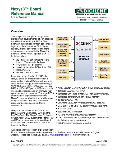
N e x y s3™B o a r d ArrayR e f e r e n c e M a n u a lRevision: July 26, 2011 1300 Henley Court | Pullman, WA 99163(509) 334 6306 Voice and FaxOverview Array The Nexys3 is a complete, ready-to-usedigital circuit development platform based onthe Xilinx Spartan-6 LX16 FPGA. TheSpartan-6 is optimized for high performancelogic, and offers more than 50% highercapacity, higher performance, and moreresources as compared to the Nexys2’sSpartan-3 500E FPGA. Spartan-6 LX16features include:•2,278 slices each containing four 6-input LUTs and eight flip-flops•576Kbits of fast block RAM•two clock tiles (four DCMs & two PLLs)•32 DSP slices•500MHz+ clock speedsIn addition to the Spartan-6 FPGA, theNexys3 offers an improved collection ofperipherals including 32Mbytes of Micron’slatest Phase Change nonvolatile memory, a10/100 Ethernet PHY, 16Mbytes of CellularRAM, a USB-UART port, a USB host port formice and keyboards, and an improved high-speed expansion connector. The large FPGAand broad set of peripherals make theNexys3 board an ideal host for a wide rangeof digital systems, including embeddedprocessor designs based on Xilinx’sMicroBlaze.Nexys3 is compatible with all Xilinx CADtools, including ChipScope, EDK, and thefree WebPack. The Nexys3 uses Digilent'snewest Adept USB2 system that offers FPGAand ROM programming, automated boardtests, virtual I/O, and simplified user-datatransfer facilities.A comprehensive collection of board supportIP and reference designs, and a large collection of add-on boards are available on the Digilentwebsite. Please see the Nexys3 page at for more information.ConfigurationAfter power-on, the Spartan-6 FPGA board must be configured (or programmed) before it can perform any functions. The FPGA can be configured in one of four ways: a PC can use the Adept "USB Prog" port to program the FPGA any time power is on; a configuration file stored in the non-volatile parallel PCM device can be transferred to the FPGA at power-on using the BPI-UP port; a file stored in the non-volatile serial (SPI) PCM device can be transferred to the FPGA using the SPI port; or a programming file can be transferred from a USB memory stick attached to the USB HID port. An on-board "mode" jumper (J8) selects between the programming modes as shown in the J8 Mode legend in the figure below.Programming files are stored in SRAM-based memory cells within the FPGA. This data defines the FPGA’s logic functions and circuit connections, and it remains valid until it is erased by removing board power, by pressing the reset button attached to the PROG input, or by writing a new configuration file using the JTAG port.FPGA configuration files transferred via the JTAG port use the .bin or .svf file types, files transferred from a USB stick use the .bit file type, and BPI or SPI programming files can use .bit, .bin, or .mcs types. The ISE/WebPack or EDK software from Xilinx can create bit, svf, bin, or mcs files from VHDL, Verilog, or schematic-based source files (EDK is used for MicroBlaze™ embedded processor-based designs). Digilent's Adept software or Xilinx's iMPACT software can be used to program the FPGA or ROMs using the Adept USB port.During JTAG programming, a .bit or .svf file is transferred from the PC to the FPGA using the Adept USB port. When programming a non-volatile PCM device, a .bit, .bin, or .mcs file is transferred to the in a two-step process. First, the FPGA is programmed with a circuit that can program PCM devices, and then data is transferred to the PCM device via the FPGA circuit (this complexity is hidden from the user – a simple “program ROM” interface is presented by the programming software. Note the PCM devices are next-generation Flash ROM devices, and they are often referred to as "Flash" or "ROM" memory). After the PCM device has been programmed, it can automatically configure the FPGA at a subsequent power-on or reset event as determined by the J8 jumper setting. Programming files stored in the PCM devices will remain until they are overwritten, regardless of power-cycle events.The FPGA can be programmed from a memory stick attached to the USB-HID port if the stickJTAG (both jumpers loaded), and board power is cycled. The FPGA will automatically reject any .bit files that are not built for the proper FPGA.After being successfully programmed, the FPGA will cause the "Done" LED to illuminate. Pressing the Reset button at any time will reset the configuration memory in the FPGA. After being reset, theFPGA will immediately attempt to reprogram itself from one of the PCM devices if the J8 Mode jumper is set to BPI or SPI mode.AdeptPowerSwitch Power JackPower Reset Power Select LEDs Slide switches Push buttons7-seg USB 10/100PmodVHDC ConncectorDigilent's Adept software offers a simplified programming interface and many additional features as described below. The Adept USB port is fully compatible with all Xilinx tools, including the iMPACT programming software. The Adept features are always available, regardless of how the FPGA was programmed.Adept SystemDigilent's Adept high-speed USB2 system can be used to program the FPGA and PCM devices, run automated board tests, add PC-based virtual I/O devices (like buttons, switches, and LEDs) to FPGA designs, and exchange register-based and file-based data with the FPGA. Adept automatically recognizes the Nexys3 board and presents a graphical interface with tabs for each of these applications. Adept also includes public APIs/DLLs so that users can write applications to exchange data with the Nexys3 board at up to 38Mbytes/sec. The Adept application, an SDK, and reference materials are freely downloadable from the Digilent website.To program the Nexys3 board using Adept, firstset up the board and initialize the software:•plug in and attach the power supply•plug in the USB cable to the PC and tothe USB port on the board•start the Adept software•turn ON Nexys3's power switch•wait for the FPGA to be recognized.Use the browse function to associate thedesired .bit file with the FPGA, and click on theProgram button. The configuration file will besent to the FPGA, and a dialog box will indicatewhether programming was successful. Theconfiguration “done” LED will light after theFPGA has been successfully configured.Before starting the programming sequence, Adept ensures that any selected configuration filecontains the correct FPGA ID code – this prevents incorrect .bit files from being sent to the FPGA.In addition to the navigation bar and browse and program buttons, the Config interface provides anInitialize Chain button, console window, and status bar. The Initialize Chain button is useful if USB communications with the board have been interrupted. The console window displays current status, and the status bar shows real-time progress when downloading a configuration file.Memory InterfaceThe Memory tab allows .bin, .bit, and .mcsconfiguration files to be transferred to the on-board BPI (parallel) or SPI (serial) PCM devicesfor subsequent FPGA programming, and allowsuser data files to be transferred to/from thePCM devices or RAM memories at user-specified addresses. The target memory isselected by clicking one of the three radiobuttons in the upper-right corner.All three memory devices (the PCM's and the cellular RAM) can be fully tested by clicking the Full Test button. They can also be completely erased by clicking the Erase button.The Read/Write tools allow data to beexchanged between files on the host PC and specified address ranges in the memory devices.Test Interface Array The test interface provides an easy way to verify many of the board's hardware circuits and interfaces. These are divided into two major categories: on-board memory (RAM and Flash) and peripherals. In both cases, the FPGA is configured with test and PC-communication circuits, overwriting any FPGA configuration that may have been present.Clicking the Run RAM/Flash Test button will identify the CellularRam, SPI Flash, and BPI Flash memory by reading out and verifying the IDCODE on each memory. The memory contents will not be modified. To run a full test on a particular memory device, refer to the Full Test in the Memory Tab.Clicking the Start Peripherals Test button will initialize GPIO and user I/O testing. Once the indicator near the Start Peripherals Test button turns green, all peripheral tests can be run.The Test Shorts feature checks all discreteI/O’s for shorts to Vdd, GND, and neighboring I/O pins. The switches and buttons graphicsshow the current states of those devices on theNexys3 board. Connect a VGA monitor and USB mouse to visually test the J2 VGA port and J4 USB port respectively.Register I/O Array The register I/O tab requires that a corresponding IP block, available in the Parallel Interface reference design (DpimRef.vhd) on the Adept page of the Digilent website, is included and active in the FPGA. This IP block provides an EPP-style interface, where an 8-bit address selects a register, and data read and write buttons transfer data to and from the selected address. Addresses entered into the address field must match the physical address included in the FPGA IP block.Register I/O provides an easy way to movesmall amounts of data into and out of specificregisters in a given design. This feature greatly simplifies passing control parameters into a design, or reading low-frequency status information out of a design.File I/O Array The File I/O tab can transfer files between the PC and the Nexys3 FPGA. A number of bytes (specified by the Length value) can be streamed into a specified register address from a file or out of a specified register address into a file. During upload and download, the file start location can be specified in terms of bytes.As with the Register I/O tab, File I/O alsorequires specific IP to be available in theFPGA. This IP can include a memory controller for writing files into the on-board Ram and Flash memories.The I/O Expand tab works with an IP block inthe FPGA to provide additional simple I/Obeyond the physical devices found on theNexys3 board. Virtual I/O devices include a 24-LED light bar, 16 slide switches, 16 pushbuttons, 8 discrete LEDs, a 32-bit register thatcan be sent to the FPGA, and a 32-bit registerthat can be read from the FPGA. The IP block,available in the Adept I/O Expansion referencedesign (AdeptIOExpansion.zip) on the Adeptpage of the Digilent website, provides a simpleinterface with well-defined signals. This IPblock can easily be included in, and accessedfrom, user-defined circuits.For more information, see the Adeptdocumentation available at the Digilentwebsite.Power SuppliesThe Nexys3 board can receive power from the Adept USB port or from an external power supply. Jumper JP1 (near the power jack) determines which source is used.The USB port can deliver enough power for the vast majority of designs. It is possible that a very demanding application, including an application that drives many peripheral boards, might require more power than can be delivered by the USB port. Some applications may also need to run without being connected to a PC’s USB port. In either case, an external power supply or battery pack can be used by setting JP1 to “Wall”.The main regulator on the Nexys3 can accommodate input voltages up to 15VDC. An external DC wall-plug supply should provide at least five watts of input power, and use a coax center-positive2.1mm internal-diameter plug. An external battery pack can also be used by connecting the battery’s terminal leads to connector J11 (J11 is in parallel with the wall-plug power jack, so if a battery pack is connected, a wall plug should not be). An external battery pack should be limited to 12VDC, and should be capable of delivering adequate power for the application.Voltage regulator circuits from Linear Technology create the required 3.3V, 2.5V, 1.8V, and 1.2V supplies from the main power input. The table below provides additional information (typical currents depend strongly on FPGA configuration and the values provided are typical of medium size/speed designs).The Nexys3 power supplies are enabled (or turned on) by a logic-level Power switch (SW8). A power-good LED (LD8), driven by the wired-OR of the “power good” outputs on the supplies, indicates that all supplies are operating within 10% of nominal.The VU output of the main power jumper (JP1) is available to the VHDC expansion connector ifjumper JP4 is loaded. Care must be taken to ensure the VUEXP delivered to any attached expansion board is the correct voltage – since VU is driven directly from an attached supply, this means a supply of the proper voltage must be used (e.g., 5V).MemoryThe Nexys3 board contains three external memories, all from Micron: a 128Mbit Cellular RAM(pseudo-static DRAM); a 128Mbit parallel non-volatile PCM (phase-change memory); and a 128Mbit serial PCM device. The Cellular RAM and parallel PCM device share a common bus, and the serial PCM is on a dedicated quad-mode (x4) SPI bus. The non-volatile PCM memories are byte and bit alterable without requiring a block erase, so they are faster and more versatile than conventional Flash in most applications. Reference designs available on the Digilent website show examples of using the Cellular RAM in asynchronous and synchronous modes, as well as examples of reading and writing both PCM devices.Nexys3 Power SuppliesSupply CircuitsDevice Amps (max/typ) 3.3V FPGA I/O, USB ports, Clocks, ROM & RAM I/O, Ethernet IC13: LTC3633 3A / 200mA 2.5V Optional voltage for Bank0 and VHDC connector IC14: LTC3619 800mA / 0mA 1.2V FPGA CoreIC13: LTC3633 3A / 0.2 to 1.0A 1.8V RAM and ROM coreIC14: LTC3619400mA / 0.1 to 0.3AThe 16Mbyte Cellular RAM (Micron part number M45W8MW16) has a 16-bit bus that supports 8 or 16 bit data access. It can operate as a typical asynchronous SRAM with read and write cycle times of70ns, or as a synchronous memory with an 80MHz bus. When operated as an asynchronous SRAM, the Cellular RAM automatically refreshes its internal DRAM arrays, allowing for a simplified memory controller (similar to any SRAM controller). When operated in synchronous mode, continuous transfers of up to 80MHz are possible.The parallel PCM device (Micron part number NP8P128A13T1760E) is organized as 8Mwords of16bits each. It contains 128 individually erasable 64K-blocks, one of which is subdivided into four 16K “parameter blocks” that can offer increased data protection. Normally, a device with a parameter block at the high end of the address space is loaded (a “top parameter” block device). The parallel PCM memory offers 115ns read cycle times, with 25ns page-mode reads within blocks. It has an internal 64-byte write buffer that can be written with 50ns cycle times, and the 64-byte buffer can be transferred to the Flash array in 120us (typical). The parallel PCM device also contains an SPI port for serial data transfer, but that function is not enabled on the Nexys3 board (the ADV and WAIT signals are connected between the FPGA and PCM, but they serve no functions).The Cellular RAM and parallel PCM share a common 16-bit data bus and 24-bit address bus. The Cellular RAM is byte addressable using the upper-byte and lower-byte signals (MT-UB and MT-LB), but the P8P PCM is configured for 16 byte operations only (it is not byte addressable). The output enable (OE) and write enable (WE) signals are shared by both devices, but each device has individual chip enable (CE) signals. Additionally, the Cellular RAM has clock (MT-CLK), wait (MT-WAIT), address valid (MT-ADV) and control register enable (MT_CRE) signals available to the FPGA for use with synchronous transfers, and the PCM device has Reset (RP#). With simple changes, the Nexys3 board can accommodate either the PCM device or the older “P33” Flash device. The signal names in the Nexys3 schematic reference the P33 device; the P33 ADV and WAIT signals are not used in by the PCM device.The 16Mbyte serial PCM device (Micron part number NP5Q128A13ESFC0E) is also bit alterable without requiring an erase cycle. It supports the legacy SPI protocol as well as the newer Quad I/O and Dual I/O protocols, at bus speeds up to 50MHz.FPGA configuration files can be written to both PCM devices, and mode settings are available to cause the FPGA to automatically read a configuration from one of these devices at power on. A Spartan-6 LX16 configuration file requires about 512Kbytes of memory, leaving about 97% of the PCM devices available for user data.Both PCM devices are loaded with configuration files at the factory. The SPI PCM device contains a file that configures the FPGA to test the Nexys3 memory devices during manufacturing, and this file isn’t needed after the board test is complete. The BPI PCM device contains a file that configures the Nexys3 with a basic user demonstration program, and it can be used to verify board functions. This same .bit file (and complete project) is available for download from the Digilent website. If Mode jumper J8 is set to BPI mode and power is applied, the user demo configuration will be loaded. The demo drives a counter on the 7-segment display, drives the user LEDs on and off when the user switches are toggled, turns off digits on the 7-segment display when user buttons are pressed, and drives an image out the VGA port. A USB mouse can be connected to J4 for a simple visual demonstration.Please refer to the manufacturer’s data sheets and the reference designs posted on Digilent’s website for more information about the memory devices.Ethernet PHYThe Nexys3 board includes an SMSC 10/100 Ethernet PHY (SMSC part number LAN8710) paired with an RJ-45 Ethernet jack with integrated magnetics. EDK-based designs can access the PHY using either the xps_ethernetlite IP core or the xps_ll_temac IP core. The Nexys3 Base System Builder (BSB) support package automatically generates a test application for the Ethernet MAC; this can be used as a reference for creating custom designs. ISE designs can use the IP Core Generator wizard to create an Ethernet MAC controller IP core. The SMSC PHY uses the MII interface and supports 10/100 Mb/s. At power-on reset, the PHY is set to the following defaults:•MII mode interface•100Base-TX with auto negotiation enabled, advertising half-duplex, with CRS active during receive•PHY address = 000Refer to the LAN8710A data sheet on the website for further information.SMSC LAN8710AOscillators/ClocksThe Nexys3 board includes a single 100MHz CMOS oscillator connected to pin V10 (V10 is the GCLK0 input in bank 2). The input clock can drive any or all of the four clock management tiles in theautomatically be rejected. Note the PIC24 reads the FPGA's mode, init, and done pins, and can drive the PROG pin as a part of the programming sequence.HID ControllerTo access the USB host controller, EDK designscan use the standard PS/2 core (non-EDK designscan use a simple state machine). Referencedesigns posted on the Digilent website show anexample of reading characters from a USBkeyboard connected to the USB host interface.Mice and keyboards that use the PS/2 protocoluse a two-wire serial bus (clock and data) tocommunicate with a host device. Both use 11-bitwords that include a start, stop, and odd parity bit,but the data packets are organized differently, andthe keyboard interface allows bi-directional data transfers (so the host device can illuminate state LEDs on the keyboard). Bus timings are shown in the figure. The clock and data signals are only driven when data transfers occur, and otherwise they are held in the idle state at logic ‘1’. The timings define signal requirements for mouse-to-host communications and bi-directional keyboard communications. A PS/2 interface circuit can be implemented in the FPGA to create a keyboard or mouse interface.KeyboardThe keyboard uses open-collector drivers so the keyboard, or an attached host device, can drive the two-wire bus (if the host device will not send data to the keyboard, then the host can use input-only ports).PS/2-style keyboards use scan codes to communicate key press data. Each key is assigned a code that is sent whenever the key is pressed. If the key is held down, the scan code will be sent repeatedly about once every 100ms. When a key is released, an F0 key-up code is sent, followed by the scan code of the released key. If a key can be shifted to produce a new character (like a capital letter), then a shift character is sent in addition to the scan code, and the host must determine which ASCII character to use. Some keys, called extended keys, send an E0 ahead of the scan code (and they may send more than one scan code). When an extended key is released, an E0 F0 key-up code is sent, followed by the scan code. Scan codes for most keys are shown in the figure. A host device can also send data to the keyboard. Below is a short list of some common commands a host might send.ED Set Num Lock, Caps Lock, and Scroll Lock LEDs. Keyboard returns FA after receiving ED, then host sends a byte to set LED status: bit 0 sets Scroll Lock, bit 1 sets Num Lock, and bit 2 sets Caps lock. Bits 3 to 7 are ignored.EE Echo (test). Keyboard returns EE after receiving EE.F3 Set scan code repeat rate. Keyboard returns F3 on receiving FA, then host sends second byte to set the repeat rate.FE Resend. FE directs keyboard to re-send most recent scan code.FF Reset. Resets the keyboard.The keyboard can send data to the host only when both the data and clock lines are high (or idle). Since the host is the bus master, the keyboard must check to see whether the host is sending data before driving the bus. To facilitate this, the clock line is used as a “clear to send” signal. If the host pulls the clock line low, the keyboard must not send any data until the clock is released. The keyboard sends data to the host in 11-bit words that contain a ‘0’ start bit, followed by 8-bits of scan code (LSB first), followed by an odd parity bit and terminated with a ‘1’ stop bit. The keyboard generates 11 clock transitions (at 20 to 30KHz) when the data is sent, and data is valid on the falling edge of the clock. Scan codes for most PS/2 keys are shown in the figure below.MouseThe mouse outputs a clock and data signal when it is moved, otherwise, these signals remain at logic ‘1’. Each time the mouse is moved, three 11-bit words are sent from the mouse to the host device. Each of the 11-bit words contains a ‘0’ start bit, followed by 8 bits of data (LSB first), followed by an odd parity bit, and terminated with a ‘1’ stop bit. Thus, each data transmission contains 33 bits, where bits 0, 11, and 22 are ‘0’ start bits, and bits 11, 21, and 33 are ‘1’ stop bits. The three 8-bit data fields contain movement data as shown in the figure above. Data is valid at the falling edge of the clock, and the clock period is 20 to 30KHz.The mouse assumes a relative coordinate system wherein moving the mouse to the right generates a positive number in the X field, and moving to the left generates a negative number. Likewise, moving the mouse up generates a positive number in the Y field, and moving down represents a negative number (the XS and YS bits in the status byte are the sign bits – a ‘1’ indicates a negative number). The magnitude of the X and Y numbers represent the rate of mouse movement – the larger the number, the faster the mouse is moving (the XV and YV bits in the status byte are movement overflow indicators – a ‘1’ means overflow has occurred). If the mouse moves continuously, the 33-bit transmissions are repeated every 50ms or so. The L and R fields in the status byte indicate Left and Right button presses (a ‘1’ indicates the button is being pressed).VGA PortThe Nexys3 board uses 10 FPGA signals to create a VGA port with 8-bit color and the two standard sync signals (HS – Horizontal Sync, and VS – Vertical Sync). The color signals use resistor-divider circuits that work in conjunction with the 75-ohm termination resistance of the VGA display to create eight signal levels on the red and green VGA signals, and four on blue (the human eye is less sensitive to blue levels). This circuit, shown in figure 13, produces video color signals that proceed in equal increments between 0V (fully off) and 0.7V (fully on). Using this circuit, 256 different colors can bedisplayed, one for each unique 8-bit pattern. A video controller circuit must be created in the FPGA to drive the sync and color signals with the correct timing in order to produce a working display system.VGA System TimingVGA signal timings are specified, published, copyrighted and sold by the VESA organization (). The following VGA system timing information is provided as an example of how a VGA monitor might be driven in 640 by 480 mode. For more precise information, or forinformation on other VGA frequencies, refer to documentation available at the VESA website.CRT-based VGA displays use amplitude-modulated moving electron beams (or cathode rays) to display information on a phosphor-coated screen. LCD displays use an array of switches that can impose a voltage across a small amount of liquid crystal, thereby changing light permittivity through the crystal on a pixel-by-pixel basis. Although the following description is limited to CRT displays, LCD displays have evolved to use the same signal timings as CRT displays (so the “signals” discussion below pertains to both CRTs and LCDs). Color CRT displays use three electron beams (one for red, one for blue, and one for green) to energize the phosphor that coats the inner side of the display end of a cathode ray tube (see illustration). Electron beams emanate from “electron guns” which are finely-pointed heated cathodes placed in close proximity to a positively charged annular plate called a “grid”. The electrostatic force imposed by the grid pulls rays of energized electrons from the cathodes, and those rays are fed by the current that flows into the cathodes. These particle rays are initiallyMouse Data Formataccelerated towards the grid, but they soon fall under the influence of the much largerelectrostatic force that results from the entirephosphor-coated display surface of the CRT being charged to 20kV (or more). The rays are focused to a fine beam as they passthrough the center of the grids, and then they accelerate to impact on the phosphor-coateddisplay surface. The phosphor surface glowsbrightly at the impact point, and it continuesto glow for several hundred microseconds after the beam is removed. The larger the current fed into the cathode, the brighter thephosphor will glow. Between the grid and the display surface, the beam passes through the neck of the CRTwhere two coils of wire produce orthogonal electromagnetic fields. Because cathode rays arecomposed of charged particles (electrons), they can be deflected by these magnetic fields. Current waveforms are passed through the coils to produce magnetic fields that interact with the cathode rays and cause them to transverse the display surface in a “raster” pattern, horizontally from left to right and vertically from top to bottom. As the cathode ray moves over the surface of the display, the current sent to the electron guns can be increased or decreased to change the brightness of the display at the cathode ray impact point.Information is only displayed when the beam is moving in the “forward” direction (left to right and top Display Surface 640 pixels per row are displayedduring forward beam trace pixel 0,639pixel 0,0pixel 479,0pixel 479,639High voltage Deflection coils Grid Electron guns(Red, Blue, Green)gun grid deflection Cathode ray tube Cathode ray。
Maya mental ray 3s渲染基础教程-火星时代视频教学总结
使用次表面散射,可以模拟一些真实的光线渗透效果,次表面散射就是让光线部分渗透到模型内然后反射回来和让部分光线穿透模型,犹如一种半透明的效果。
次表面散射原理图在mental ray材质里misss都是次表面散射材质节点,也称SSS或3S材质,引入次表面散射材质节点后,会自动建立连接一个灯光贴图,有些不会,这个灯光贴图对于次表面散射的运行是必不可少的,因为它可以读取灯光的照明信息,然后显示在材质上,和最终聚集的原理在相似性。
次表面散射效果完全由材质本身产生,不用在渲染设置中进行任何设置,也就是次表面散射效果与渲染设置里的设置无关,使用mental ray次表面散射材质只用使用mental ray渲染。
次表面散射与灯光有很重要的关联,所以使用次表面散射是注意灯光的摆放位置,且至少要两个灯光,左右各一个,次表面散射的强弱也与灯光的强度在关。
常用的次表面散射材质是(misss_fast_simple_maya),(misss_fast_simple_maya)次表面散射材质不能直接连接置换贴图,要把材质的节点都显示出来,然后双击最高级别的节点,也就最右边的节点,然后把置换贴图节点连接到属性上的(置换材质)就可以把置换贴图连接到次表面散射的材质上,而凹凸贴图要连接到次表面散射材质属性里的(Bump Shader)-(Bump)上,但有些次表面散射材质不能直接进行凹凸贴图的连接,如(misss_fast_shader),要建立一个(misss_set_normal)节点作为贴图与次表面散射材质连接的桥梁,把凹凸贴图连接到(misss_set_normal)属性里的(Normal Vector)法线矢量上,再把(misss_set_normal)节点连接到次表面散射材质的(Bump)属性上。
在(misss_fast_simple_maya)次表面散射材质属性里(Unscattered Diffuse layer)集中的漫反射涂层-(Ambient)是控制环境对次表面散射材质照明的强弱,也可以理解成是控制物体的亮度,一般上不会使用此属性。
NX3机床模拟简易教程
机床模拟及机床构造器简易教程(机床模拟部分)由于NX3本身带有3轴至5轴的铣床,且机床模拟的过程比较简单,有助于对机床构造器的理解,所以下面先进行机床模拟的讲解。
以下为以NX3自带机床进行模拟的操作过程:1,打开NX3的加工文件,生成相应的加工程序。
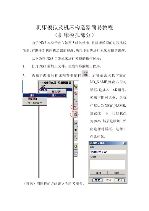
2,选择资源条的机床配置器图标,右键单击名称下面的NO_NAME,弹出右图对话框,选插入—>K组件。
弹出下图对话框,名称栏默认为NEW_NAME,建议改一下,比如我改为part,然后选添加,弹出选择对话框,选择工件几何体。
(可选)用同样的方法建立毛坯K组件。
3,此时的导航栏应如左图所示,然后在part节点上右键单击,弹出菜单上选择分类,出现右图对话框,勾选其中的_part,_setup_element项也自动被选中。
若有毛坯K组件,则将其分类为_workpiece.4,如第3步左图所示,在part节点右击,选择联接点,弹出左图对话框,选添加,建议更改一下联结点的名称,然后选定义CSYS,弹出坐标第构造器对话框,构造坐标系,此坐标系应与将要模拟刀路程序的加工坐标系一致,确认。
5,现在的导航栏应如下图所示,到此已做好调入机床的准备工作。
6切换到加工导航条并转到刀具视图,右键单击最顶部的根节点GENERIC_MACHINE ,如下左图示,选编辑,弹出如下右图示通用机床对话框。
选替换机床,弹出库类选择,选MILL ,确定,弹出机(其中的FAGOR8025为自定义的机床,默认库中没有),选sim010101_001_mm,这是一个三轴铣床,选确定,返回通用机床对话框,确定。
7,此时绘图区应有机床的显示了(若没有,请将层1设置为可见),并且工件已摆放在合适位置(这时联结点与分类共同作用的结果),导航器的的根节点也应如右图示,变为SIM010101_001_MM,展开其下的程序列表,右键单击,选刀轨—>模拟…,弹出下图中右面的对话框。
8,下面的操作我想不用多说了,其中的选项含义都很明了的!关于机床模拟的简略教程到此为止,如果大家觉得有用请跟贴鼓励,有什么疑问请与我联系q_x_j@马上会有机床构造器教程贴出,敬请关注!。
探索III游戏CE教程(图文并茂-升级打装备利器)
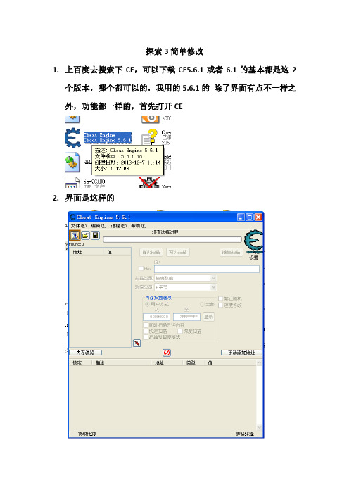
探索3简单修改1.上百度去搜索下CE,可以下载CE5.6.1或者6.1的基本都是这2个版本,哪个都可以的,我用的5.6.1的除了界面有点不一样之外,功能都一样的,首先打开CE2.界面是这样的3.然后打开探索3游戏,进入游戏以后,用CE读取游戏进程可以点击菜单进程选择也可以点击左上角文件菜单下面的小电脑图标选择,都一样从里面找到探索3的程序,有的机器可能不识别字体会出现乱码,只要知道是哪个图标就可以了。
4.选择以后就会进入一下的界面遭遇到几只怪就从上图红圈的地方(值)下面打几,然后点首次扫描如图所示继续遭遇怪这次是2只就搜索2,点再次扫描如图继续遭遇这次是1,就搜索1了,点再次扫描如图搜索1以后就剩下一个地址了这个地址就是我们需要的怪的数量的地址,接着双击这个地址,拉倒下面的地址栏,如下图:然后我们继续,遭遇怪去遇到1只,这次搜素主要是锁定几只怪怪爆装备,这次要进行新的扫描了,如果遇到1只就搜索20,2只就搜索21,3只22,以此类推1只怪搜20 继续遭遇基本上3次左右就会剩下一个地址的2只搜索21如下图双击剩下的地址拉倒下面来这时候2个地址就搜索结束了,接着就是4字节修改了双击图中值下面的数字分别把2个值改成6和26改完把前面锁定点上对勾就锁定好了这时候会弹出一个保存选项,但是千万别点这个保存,点了就会关机的务右键点击任务栏,然后点击任务管理器选中探索3游戏然后点结束进程就可以了,这时候就不会出现关机或者重启的问题了接着进入游戏这时候数据溢出你的攻击防御很多数据会变成好几亿的,有正的也有负数,最好都是整数,这样杀怪的时候不会总是出现负的经验值,我的是道士,无法打怪的,一打怪就会出现错误自动退出游戏了,道士和战士是一样的,只能是法师,法师的自动攻击对应魔攻,所以保证魔攻是整数就可以了,如果你的魔攻是负数,有两种方法解决,1)是取下一件身上的装备,我一般取下勋章,如果变正了就好,如果数据恢复正常了,那么就用第二种方法;2)继续用任务管理器结束任务,然后读取游戏,上线看数据,是负的继续取下一件装备,是正的就不用取下装备了,总之这2种方法直到把数据变正数为止。
雷曼克斯骁龙X3键盘型的手动调频教程

骁龙X3键盘型手动调频教程注意:(按一下#号键就可以完成频率模式和信道模式的切换)如果您是公司使用,为了便于您管理对讲机防止调乱,可以执行以下操作:对讲机调到信道模式下,按住井号键不松手的同时,旋转旋钮开机,您的对讲机就会进入全信道模式。
然后按住 * 号键不松手,把键盘上个锁。
1、调频率首先把对讲机调到频率模式才可以输入频率频率模式下屏幕显示的是6个数字,如果六个数字下面还有个小数,说明那是信道模式.如果旋转旋钮开机不是频率模式,请执行以下操作(按一下#号键就可以完成频率模式和信道模式的切换)(注:在调频率的时候,或许有些客户在输入频率的过程中会出现后面三位数怎么输入都输入不了想要的数值。
这样一来我们就要在菜单里面更改步进频率了。
步进频率的设置在下面会提到。
)设置步进频率请翻到说明书第十五页2、亚音频的取消1)在对讲机频率一致的情况下,A对讲机呼叫,其他对讲机可以收到,但是其它对讲机呼叫A对讲机,A对讲机收不到,这种情况一般是A对讲机设置了亚音频,只要把亚音频取消就可以了。
2)您看一下您的X3Q对讲机屏幕右下角是不是有QT或者DT,如果有,那您的X3Q对讲机设置了亚音频。
您按一下MENU键,然后按7然后按*键,然后按下箭头选到OFF,最后按一下MENU键,这样QT或者DT就消失,这样就可以收到他们讲话了。
3、亚音频的设置接收信令设置:按MENU+7,然后通过上下三角形箭头来切换模拟亚音,(*号键是切换模拟和数字亚音,#号键是切换正码N和反码I),找到您要的亚音之后按MENU确定退出;发射信令设置:按MENU+8,然后通过上下三角形箭头来切换模拟亚音,找到您要的亚音之后按MENU确定退出。
4、信道存储详见说明书18页存储新信道1.对讲机必须在频率模式下才能进行存储信道操作。
2.按下menu键,再按下※号键,进入存储信道的操作,小信道号和F标志闪烁。
3.可通过上下箭头键选择要存储的信道,或者通过直接输入数字选择要存入的信道。
- 1、下载文档前请自行甄别文档内容的完整性,平台不提供额外的编辑、内容补充、找答案等附加服务。
- 2、"仅部分预览"的文档,不可在线预览部分如存在完整性等问题,可反馈申请退款(可完整预览的文档不适用该条件!)。
- 3、如文档侵犯您的权益,请联系客服反馈,我们会尽快为您处理(人工客服工作时间:9:00-18:30)。
实验一Nexys 3 实验板及设计软件A1.1 实验简介Nexys3实验板专门由Xilinx大学合作计划(XUP)为各种层次的大学工科培养计划设计,由美国Digilent公司()制作。
因ISE软件版本不同,读者所用软件的菜单排列与名称可能与本实验介绍的略有不同,但其功能基本相同。
读者可以参考本实验提供的软件使用细节。
A1.2 实验目的熟悉Nexys3实验板使用和芯片设计流程,熟悉使用下列软件:·MATLAB/Simulink(作者使用R2010b)。
·System Generator(作者使用13.2)。
·ISE(10.1之前版本,作者使用13.2)。
·ChipScope(与ISE相应版本,作者使用13.2)。
·Xilinx ISE Simulator或ModelSim(Mentor Graphics软件)。
学习从电路设计到比特流下载全过程,学习使用ChipScope观察来自芯片的信号波形。
A1.3 实验任务本实验由3部分组成:第一部分学习使用Simulink,学习用Simulink元件和Xilinx元件搭建电路模型,熟悉使用Simulink软件界面;第二部分学习使用System Generator(SysGen)和ISE工具,学习基于Simulink模型的综合流程,熟悉ISE工具环境和使用SysGen生成的设计工程文件,学习使用布局布线工具和FPGA编辑器,学习阅读综合报告等;第三部分学习将物理综合结果下载到FPGA芯片,学习下载前VHDL行为方针,学习用ChipScope观察比特流下载后来自芯片的波形。
A1.4 实验步骤第一部分:Simulink 与Xilinx设计单元库的使用1.启动MTALAB,指定一个工作目录(如F:\FPGA\DSP\LAB1)为当前目录(见图A1.1)。
图A1.1 MATLAB Simulink 的启动按钮与当前目录窗口2.单击MATLAB工具栏内的Simulink按键(见图A1.1),或在MATLAB命令行中输入simulink。
这时弹出Simulink Library Browser(见图A1.2)。
图A1.2 Simulink单元库浏览器3.选择File→New→Model命令,打开新建模型编辑器。
4.在Simulink Library Browser中浏览Xilinx Blockset(见图A1.3),选择Basic Elements选项。
从右边的元件窗口将以下图标拖曳到模型编辑器中从Xilnx Blockset目录下的Index栏目下找到延迟(Delay)单元放入编辑器。
从Simulink目录下的Sources栏目找到Constant 单元,从同一目录下的Sinks栏目找到Scope单元,均放入电路编辑器。
图A1.3 Xilinx Blocks菜单及当前电路5.连接各模块:在Constant单元的输出端口按下鼠标左键,拉到Gateway In单元的输入端口。
连接成功后鼠标箭头的单线十字变为双线十字,放开鼠标左键后连接线由虚线变为实线。
所有单元前后连接完成后得到如图A1.4所示的电路。
将模型保存到文件delay1.mdl。
放入的System Generator图标用于设置仿真参数和设计综合,不必连接到电路。
图A1.4 延迟单元与输入输出单元组成的电路(delay1.mdl)6.为比较输入与输出波形,可以在信号源Constant与Gateway In之间连接另一个Scope(见图A1.5a),或者接一个双输入端口Scope(见图A1.5b)。
双击打开Scope,单击Scope 窗口上沿第二个工具图标Parameters,打开窗口后,在Numbers of axes 文本框中填入2,单机OK按钮后Scope的输入端口变为两个。
如图A1.5b所示为将Scope输入端口之一接Constant输出。
图A1.5a 输入端接另一个Scope图A1.5b 比较输入输出波形(delay2.mdl)7.仿真之前先设置各单元的参数。
双击各元件弹出参数设置窗口。
图A1.6为Gateway In的参数设置窗口。
Gateway In相当与一个采样量化装置,用户可以选择采样周期(Sample period)、量化位宽(Number of bits)、对量化(Quantization)的处理(Truncate/Round)和对溢出(Overflow)的处理(Wrap/Saturate)等。
如图A1.6所示设置Gateway In的参数:位宽为8,小数位为0,Overflow设为Wrap,采样周期为1(默认值)。
打开Constant 单元查看参数为单位阶跃输入(保持默认值不变)。
双击延迟单元查看延迟单位(Latency)为1(默认值)。
Gateway Out的功能是把8位定点数转化为浮点数后输出给Scope上。
打开Gateway Out确认Translate into output 选项已被选中,保持参数不变。
图A1.6 Gateway In参数设置8.Simulink工具栏系统仿真时间设置为默认值10.0(以仿真时钟周期为单位,可以根据需要修改)。
单击Simulink仿真按钮▶开始仿真。
双击Scope观察输出波形。
如图A1.7所示为图A1.5b所示电路双端口Scpoe上显示的波形,上半部为输入波形,下半部为输出波形,可以看到输出波形延迟了1单位时间。
可以用Scope工具栏里提供的按钮调整坐标范围和缩放波形等。
将电路模型重新保存为delay2.mdl。
图A1.7 双输入Scope显示的波形9.在Simulink Sources目录下找到正弦信号(Sine wave)单元放入电路图。
删除Constant单元,用正弦信号单元代替常数单元接到Gateway In输入。
打开Sine Wave单元,设置参数如下:幅度(Amplitude)为50,频率(Frequency)为2*pi*100,采样时间(Sample time)为1e-4(即采样频率为10kHz)(见图A1.8)。
同时设Gateway In的Sample period 为1e-4。
打开System Generate模块,将Simulink system period时间也设为1e-4。
打开延迟单元将Latency 改为10。
将Simulink仿真时间改为0.02(即2个正弦波周期)。
图A1.8 Sine Wave参数设置10.单机仿真按钮,在Scope中看到如图A1.9所示的波形。
分析观察到的延迟是否与电路设计一致。
将仿真正确的电路保存为sinewave.mdl。
图A1.9 Scope显示输入输出正弦波形11.调整设计:改变正弦信号波形(幅度、频率、采样频率),改变延迟单元时延长度,改变仿真运行时间等,分别观察仿真波形输出的变化,记录仿真结果。
注意:改变Gateway In采样频率时要相应调整System Generator中的Simulink system period设置,一般应保持一致,否则仿真时系统可能会提示错误。
12.将正弦波幅度从50改为150,再次仿真,观察输出波形的变化。
改变Gateway In模块关于Overflow的选项Wrap和Saturate,然后重新仿真,观察仿真结果的变化并做出解释。
第二部分:System Generator 与ISE的使用1.再次打开电路模型delay1.mdl。
2.双击System Generator图标后弹出System Generator的参数设置窗口(见图A1.10)。
可设置的参数包括:编译生成的网表格式(HDL Netlist)、工具支持的FPGA芯片型号(这里使用Nexys3板子的芯片Spartan6 xc6slx16-2csg324)、生成工程文件的目标目录(Target directory,默认目录./netlist)、综合工具(XST)、硬件描述语言(VHDL或Verilog)。
在时钟标签下参数包括:产生时钟信号的引脚名称(V10,依赖于芯片型号和系统板)。
FPGA clock period 是Simulink仿真时间步长,一般System Generator中的Simulink system period 时间要与Gateway In参数Sample period时间一致。
图A1.10a Sy sGen参数设置图A1.10b SysGen参数设置3.因System Generate 综合后将产生大量的文件,为便于管理工程,建议为每一个电路建立一个目录。
例如,为电路delay1.mdl建立一个delay1目录。
System Generator生成文件将保存与delay1/netlist下。
4.参数设置完毕之后单击System Generator窗口中的Generate按钮。
System Generator开始编译,编译成功后在目标目录./netlist下将生成一系列项目文件。
目录下的部分文件是ISE综合时的输入文件。
ISE读入这些文件后综合生成用于FPGA芯片物理实现的比特流。
5.双击桌面上的ISE图标或从“开始”菜单中启动ISE工具(作者使用ISE13.2版)。
6.执行File Open Project命令,可以浏览到delay工程所在的目录。
打开工程文件delay1_cw.ise(见图A1.11)。
Hierarchy窗口中列出的是与该工程有关的源文件。
Processes 窗口中列出的是用于FPGA物理综合的系统工具,本实验中只介绍其中一部分。
图A1.11 打开工程后的ISE窗口7.展开Processes窗口中的Implement Design目录,看到Place & Route子目录(见图A1.12)。
进一步展开Place & Route,右击Generate Post-Place & Route Static Timing 选择Run命令。
这时ISE开始编译综合,在位于下方的Console窗口将显示运行过程信息。
运行结束后在Console窗口中将显示如图A1.13所示的信息。
运行结束后在目录前标上绿色记号表示该条目已顺利运行结束。
同时可以看到在工程目录delay下又增加了一些新生成的目录和文件,这些都是编译综合过程中各种工具生成的中间文件。
图A1.12 Processes窗口各级目录图A1.13Post-Place & Route成功结束信息8.在Processes窗口的最上方双击Design Summary/Reports,在Detailed Reports中选择Placeand Route Report。
其中显示了如图A1.14所示的资源使用报告等信息。