QX5305规格书
MIC5305中文资料
August 2004
3
M9999-081704
元器件交易网 MIC5305 Absolute Maximum Ratings(1)
Supply Input Voltage (VIN) .................................... 0V to 6V Enable Input Voltage (VEN) ................................... 0V to 6V Power Dissipation (PD) ........................ Internally Limited(3) Junction Temperature(TJ) ........................ –40°C to +125°C Storage Temperature (TS) ......................... –65°C to 150°C Lead Temperature (soldering, 5 sec.) ....................... 260°C ESD(4) .............................................................................................. 2kV
Note: 1. For other output voltage options, contact Micrel marketing. 2. Please contact Micrel marketing regarding availability.
Micrel
Marking 815 N815 818 N818 825 N825 826 827 828 82J N82J 829 N829 830 N830 833 84H 8AA
群创奇美5.6寸工业液晶屏AT056TN52规格书-深圳德路西电子有限公司

INNO L U X DISPLAY CORPORATIONLCD MODULESPECIFICATIONCustomer:Model Name: AT056TN52 V.3SPEC NO.: A056-52-TT-31Date: 2009/03/25Version: 01■Preliminary Specification□Final SpecificationFor Customer’s AcceptanceApproved by CommentApproved by Reviewed by Prepared byJoe Lin 2009/03/31Jack HuangCharlie ChouJames Yu2009/03/30David Lee2009/03/26The copyright belongs to InnoLux. Any unauthorized use is prohibited.InnoLux copyright 2004All rights reserved,Copying forbidden.Record of RevisionVersion Revise Date Page ContentPre-spec.01 2009/03/25 Initial ReleaseContents:1.General Specifications (1)2.Pin Assignment (2)3.Operation Specifications (5)3.1.Absolute Maximum Ratings (5)3.2.Typical Operation Conditions (6)3.2.1 Typical Operation Conditions (6)3.2.2 Current Consumption (6)3.2.3 Backlight Driving Conditions (7)3.3.Power Sequence (8)3.4.Timing Characteristics (9)3.4.1.Timing Conditions (9)3.4.2.Timing Diagram (11)4.Optical Specifications (14)5.Reliability Test (18)6.General Precautions (19)6.1.Safety (19)6.2.Handling (19)6.3.Static Electricity (19)6.4.Storage (19)6.5.Cleaning (19)7.Mechanical Drawing (20)8.Package Drawing (21)8.1.Packaging Material Table (21)8.2.Packaging Quantity (21)8.3.Packaging Drawing (22)Page : 1/22 1.General SpecificationsNo. Item Specification Remark1 LCD size 5.6 inch(Diagonal)2 Driver element a-Si TFT active matrix3 Resolution 640 × (RGB) × 4804 Display mode Normally White, Transmissive5 Dot pitch 0.0588(W) × 0.1764(H) mm6 Active area 112.896 (W) × 84.672(H) mm7 Module size 126.5(W) × 100(H) × 5.7(D) mm Note 18 Surface treatment Anti-Glare9 Color arrangement RGB-stripe10 Interface Digital11 Backlight Power consumption0.930W12 Panel Power consumption 117mW13 Weight 132gNote 1: Refer to Mechanical Drawing.Page : 2/22 2.Pin AssignmentTFT LCD Panel Driving SectionFPC connector is used for the module electronics interface. The recommended model isFH12S-50S-0.5SH manufactured by HiRose.Pin No.Symbol I/O Function Remark1 V LED+P Power for LED backlight anode2 V LED+P Power for LED backlight anode3 V LED-P Power for LED backlight cathode4 V LED-P Power for LED backlight cathode5 GND P Power ground6 V COM I V COM input7 V CC P Digital power supply(+3.3V)8 MODE I DE or HV mode control Note 19 DE I Data Enable10 VS I Vsync signal input11 HS I Hsync signal input12 B7 I Blue data input (MSB)13 B6 I Blue data input14 B5 I Blue data input15 B4 I Blue data input16 B3 I Blue data input17 B2 I Blue data input18 B1 I Blue data input19 B0 I Blue data input(LSB)20 G7 I Green data input(MSB)21 G6 I Green data input22 G5 I Green data input23 G4 I Green data input24 G3 I Green data input25 G2 I Green data input26 G1 I Green data input27 G0 I Green data input(LSB)28 R7 I Red data input(MSB)29 R6 I Red data inputPage : 3/2230 R5 I Red data input31 R4 I Red data input32 R3 I Red data input33 R2 I Red data input34 R1 I Red data input35 R0 I Red data input(LSB)36 GND P Power ground37 DCLK I Sample clock38 GND P Power ground39 L/R I Select left to right scanning direction Note 2,340 U/D I Select up or down scanning direction Note 2,341 VGH I Positive power for scan driver42 VGL I Negative power for scan driver43 AV DD P Power supply for analog circuit44 RESET I Reset45 POL O Polarity select for the line inversion control signal46 V COM I V COM input47 NC - No Connector48 NC - No Connector49 NC - No Connector50 NC - No Connector Note:I: input, O: output t, P: Power , R: ReserveNote 1: DE Mode, Mode=”H”,HS floating and VS floating HV Mode, Mode=”L” and DE floatingNote 2: Selection of scanning modeSetting of scan control inputU/D L/RScanning direction GND V CC Up to down, left to right V CC GND Down to up, right to left GND GND Up to down, right to left V CC V CC Down to up, left to rightPage : 4/22 Note 3: Definition of scanning direction.Refer to the figure as below:Left RightUpDownPage : 5/22 3.Operation Specifications3.1. Absolute Maximum Ratings(Note 1)ValuesItem SymbolMin. Max.Unit RemarkV CC-0.3 6.5 VAVDD-0.3 6.5 VV GH-0.318 VV GL-150.3 V Power voltageV GH-V GL- 33 V Operation temperature T OP-2070 ℃Storage temperature T ST-3080 ℃Note 1: The absolute maximum rating values of the module should not be exceeded.Once exceeded absolute maximum rating values, the characteristics of themodule may not be recovered. Even in an extreme condition, may result inmodule permanently destroyed.Page : 6/22 3.2.Typical Operation Conditions3.2.1 Typical Operation ConditionsValuesItem SymbolUnit RemarkMin. Typ. Max.V CC 3.0 3.3 3.6 V Note 1AV DD 4.8 5.0 5.2 VPower voltageV GH14.3 15.0 15.7 VV GL-10.5-10.0-9.5VV CAC- 5.50 - VV COMV CDC0.72 0.92 1.12 VInput logic high voltage V IH0.7V CC- 1V CC VNote 2 Input logic low voltage V IL0 - 0.3V CC VNote 1: V CC setting should match the signals output voltage (refer to Note 2) of customer’s system board.Note 2: DCLK,DE, HS, VS, R0~ R7,G0~ G7,B0~ B7.3.2.2 Current Consumption(GND =0V)ValuesUnit Remark Item SymbolMin.Typ. Max.I GH- 120 240 uA V GH =+15VI GL- 130 260 uA V GL = -10V Current for DriverI CC- 10 15 mA V CC =3.3VI DD- 16 24 mA AV DD =5VPage : 7/223.2.3 Backlight Driving ConditionsValuesUnit Remark Item SymbolMin. Typ. Max.Voltage for LED Backlight V L8.4 9.3 10.5 V Note 1 Current for LED Backlight I L90 100 110 mALED life time - 20,000- - Hr Note 2Note 1: The Voltage for LED Backlight is defined at Ta=25℃ and I L =100mA.Note 2: The “LED life time” is defined as the module brightness decrease to 50% original brightness that the ambient temperature is 25℃ and I L =100mA. The LED lifetimecould be decreased if operating I L is lager than 100 mA.Page : 8/22 3.3. Power Sequence3.3.1 Power on:VGHB/LAVDDVCCDATAGNDVGLTT=0G/2Note:Data includes DE, VS ,HS,B0~B7,G0~G7,R0~R7,DCLK.VCC→VGL→VGH→Data→B/LB/L→Data→VGH→VGL→VCCPage : 9/22 3.4.Timing Characteristics3.4.1.Timing ConditionsInput/Output TimingValuesUnit. Remark Item SymbolMin.Typ. Max.PXLCLK clock time Tclk 33.339.7 - nsPXLCLK pulse duty Tcwh 40 50 60 % TclkDATA set-up time Tdsu 12 - - ns DATA to PXLCLK DATA hold time Tdhd 12 - - ns DATA to PXLCLK DE setup time Tesu 12 - - ns DE to PXLCLK VSYNC setup time Tvst 12 - - nsVSYNC hold time Tvhd 12 - - nsHSYNC setup time Thst 12 - - nsHSYNC hold time Thhd 12 - - nsHSYNC period time Th 22.9131.76- usHSYNC width Thwh 1 - - TclkVSYNC width Tvwh 1 - - ThHSYNC to CLKIN Thc - - 1 TclkDE Mode input Timing LimitationValuesUnit Remark DE ModeMin. Typ. Max.THC 48 160 765 tclkTHD 640 640 640 tclkTH 688 800 1405 tclk 1TH=1lineTVC 6 45 255 lineTVD 480 480 480 lineTV 486 525 735 line 1TV=1fieldPage : 10/22 HV Mode input Timing LimitationValuesUnit RemarkHV ModeMin. Typ. Max.Thwh - 10 - tclkThbp - 134 - tclkThfp - 16 - tclkTHD - 640 - tclkTH - 800 - tclk 1TH=1 lineTvwh - 2 - lineTvbp - 11 - lineTvfp - 32 - lineTVD - 480 - lineTV - 525 - line 1TV=1 fieldPage : 11/22 3.4.2.Timing DiagramFig.3-2 DE Mode Input TimingFig.3-3 HV Mode Input TimingPage : 14/22 4.Optical SpecificationsValuesItem Symbol ConditionMin.Typ.Max.Unit RemarkθLΦ=180°(9 o’clock)60 70 -θRΦ=0°(3 o’clock) 60 70 -θTΦ=90°(12 o’clock)40 50 -Viewing angle(CR≥10)θBΦ=270°(6 o’clock)60 70 -degree Note 1T ON- 10 20 msec Note 3 Response timeT OFF-1530msec Note 3 Contrast ratio CR 400500-- Note 4W X 0.260.310.36-Color chromaticityW Y0.280.330.38-Note 2Note 5Note 6 Luminance L 150200- cd/m² Note 6 Luminance uniformity Y UNormalθ=Φ=0°7075-% Note 6,7 Test Conditions:1.V CC=3.3V, I L=100mA, the ambient temperature is 25.℃2.The test systems refer to Note 2.Page : 15/22Note 1: Definition of viewing angle rangeFig. 4-1 Definition of viewing angleNote 2: Definition of optical measurement system.The optical characteristics should be measured in dark room. After 30 minutes operation, the optical properties are measured at the center point of the LCD screen. (Response time is measured by Photo detector TOPCON BM-7, other items are measured by BM-5A/Field of view: 1° /Height: 500mm.)Fig. 4-2 Optical measurement system setupNormal line θ=Φ=0°Normal line θ=Φ=0°Photo detectorΦ=90°12 o’clock directionΦ=270°6 o’clock directionΦ=0°Φ=180°Active Area500mmLCD PanelΦ=90°12 o’clock directionΦ=270°6 o’clock directionΦ=0°Φ=180°Active Area θL θTθBθRNote 3: Definition of Response timeThe response time is defined as the LCD optical switching time interval between“White” state and “Black” state. Rise time (T ON) is the time between photo detector output intensity changed from 90% to 10%. And fall time (T OFF) is the timebetween photo detector output intensity changed from 10% to 90%.Fig. 4-3 Definition of response timeNote 4: Definition of contrast ratiostateBlack""theonisLCDwhenmeasuredLuminancestateWhite""theonisLCDwhenmeasuredLuminance=(CR)ratioContrastNote 5: Definition of color chromaticity (CIE1931)Color coordinates measured at center point of LCD.Note 6: All input terminals LCD panel must be ground while measuring the center area of the panel. The LED driving condition is I L=100mA .100%90%10%0%Photodetectoroutput(Relativevalue)ONTWhite (TFT OFF)Black (TFT ON)White (TFT OFF)Note 7:Definition of Luminance UniformityActive area is divided into 9 measuring areas (Refer to Fig. 4-4 ).Every measuring point is placed at the center of each measuring area.maxminBB(Yu)UniformityLuminance=L-------Active area length W----- Active area widthWW/3W/3W/6L/3L/3L/6LFig. 4-4 Definition of measuring pointsB max: The measured maximum luminance of all measurement position.B min: The measured minimum luminance of all measurement position.5.Reliability Test(Note3)Item Test Conditions Remark High Temperature Storage Ta = 80℃240 hrs Note 1, 4 Low Temperature Storage Ta = -30240hrs℃Note 1, 4High Temperature Operation Ts = 70240hrs℃Note 2, 4Low Temperature Operation Ta = -20240hrs℃Note 1, 4Operate at High Temperature and Humidity +40, 90%RH240 hrs℃Note 4Thermal Shock -30/30 min ~ +℃80/30 min for a total 100℃cycles, Start with cold temperature and endwith high temperatureNote 4Vibration Test Frequency range:10~55Hz Stroke:1.5mmSweep:10Hz~55Hz~10Hz2 hours for each direction of X. Y. Z.(6 hours for total)Mechanical Shock 100G 6ms,±X, ±Y, ±Z 3 times for each directionPackage Vibration Test Random Vibration :0.015G*G/Hz from 5-200HZ, -6dB/Octave from 200-500HZ2 hours for each direction of X. Y. Z.(6 hours for total)Package Drop Test Height:60 cm1 corner, 3 edges, 6 surfacesElectro Static Discharge ± 2KV, Human Body Mode, 100pF/1500ΩNote 1: Ta is the ambient temperature of samples.Note 2: Ts is the temperature of panel’s surface.Note 3: In the standard condition, there shall be no practical problem that may affect the display function. After the reliability test, the product only guaranteesoperation, but doesn't guarantee all the cosmetic specification.Note 4: Before cosmetic and function tests , the product must have enough recovery time, at least 2 hours at room temperature.6.General Precautions6.1.SafetyLiquid crystal is poisonous. Do not put it in your mouth. If liquid crystal touches your skin or clothes, wash it off immediately by using soap and water.6.2.Handling1.The LCD panel is plate glass. Do not subject the panel to mechanical shock or toexcessive force on its surface.2.The polarizer attached to the display is easily damaged. Please handle it carefullyto avoid scratch or other damages.3.To avoid contamination on the display surface, do not touch the module surfacewith bare hands.4.Keep a space so that the LCD panels do not touch other components.5.Put cover board such as acrylic board on the surface of LCD panel to protect panelfrom damages.6.Transparent electrodes may be disconnected if you use the LCD panel underenvironmental conditions where the condensation of dew occurs.7.Do not leave module in direct sunlight to avoid malfunction of the ICs.6.3.Static Electricity1.Be sure to ground module before turning on power or operating module.2.Do not apply voltage which exceeds the absolute maximum rating value.6.4.Storage℃1.Store the module in a dark room where must keep at +25±10 and 65%RH orless.2.Do not store the module in surroundings containing organic solvent or corrosivegas.3.Store the module in an anti-electrostatic container or bag.6.5.Cleaning1.Do not wipe the polarizer with dry cloth. It might cause scratch.2.Only use a soft sloth with IPA to wipe the polarizer, other chemicals mightpermanent damage to the polarizer.Page : 20/22 7.Mechanical DrawingPage : 21/22 8.Package Drawing8.1.Packaging Material TableNo.ItemModel(Material)Dimensions(mm)UnitWeight(kg)Quantity Remark1 LCMModuleAT056TN52 V.3 126.5 × 100 × 5.7 0.132 60pcs2 Partition B Corrugatedpaper105 × 349 0.031 8pcs3 CorrugatedBoardB Corrugatedpaper510 × 350 0.074 2pcs4 PartitionPaperBC Corrugatedpaper512 × 226 × 349 1.000 1set5 Dust-ProofBagPE 700 × 530 0.060 1pcs6 A/S Bag PE 170 × 110 × 0.2 0.002 60pcs7 Carton Corrugated paper530 × 355 × 255 0.810 1 pcs8 Total Weight10.306 ± 5% kg8.2.Packaging QuantityTotal LCM quantity in Carton: no. of Partition 4 Rows x quantity per Row 15= 60Page : 22/22 8.3. Packaging Drawing。
摩克(Moxa)TN-5305系列EN501555-口IP67无管理Ethernet开关产品介绍说明

TN-5305SeriesEN501555-port IP67unmanaged Ethernet switchesFeatures and Benefits•10/100BaseT(X),4-pin M12(D-coded),F/H duplex mode,and auto MDI/MDI-X connection•IP67-rated housing protection•Power input:12to45VDC,18to30VAC•Complies with all EN50155mandatory test items1•-40to75°C operating temperature range(-T models)CertificationsIntroductionThe TN-5305Series Ethernet switches are IP67-rated for tough industrial applications.By using M12connectors,you can rest assured that Ethernet cables will connect tightly to the switch,and will be robust enough to protect your applications from external disturbances,such as the vibration and shock encountered in the transportation industry.The space-saving TN-5305switches can be mounted virtually anywhere,and wide operating temperature(-40to75°C)models are also available for use in the most extreme weather conditions.TN-5305Series Ethernet switches comply with a portion of EN50155specifications,covering operating temperature,power input voltage,surge,ESD,and vibration,making the switches suitable for a variety of industrial applications.SpecificationsEthernet Interface510/100BaseT(X)Ports(M12D-coded4-pin femaleconnector)Standards IEEE802.3for10BaseTIEEE802.3u for100BaseT(X)IEEE802.3x for flow controlPower ParametersInput Current0.1A@24VDC,0.08A@36VDCInput Voltage18to30VAC(47to63Hz)24to36VDCNo.of Power Inputs1Operating Voltage18to30VAC12to45VDCPower Connector M12A-coded male connectorPhysical CharacteristicsHousing Plastic top cover,metal bottom plateIP Rating IP671.This product is suitable for rolling stock railway applications,as defined by the EN50155standard.For a more detailed statement,click here:/doc/specs/EN_50155_Compliance.pdfDimensions60x125x29.6mm(2.36x4.92x1.09in) Weight Packaged:270g(0.56lb)Installation DIN-rail mounting(with optional kit)Wall mountingEnvironmental LimitsOperating Temperature TN-5305:-25to60°C(-13to140°F)TN-5305-T:-40to75°C(-40to167°F)Storage Temperature(package included)-40to85°C(-40to185°F)Ambient Relative Humidity5to95%(non-condensing)Altitude2000mStandards and CertificationsFreefall IEC60068-2-32EMC EN55032/35EMI CISPR32,FCC Part15B Class AEMS IEC61000-4-2ESD:Contact:6kV;Air:8kVIEC61000-4-3RS:80MHz to1GHz:20V/mIEC61000-4-4EFT:Power:2kV;Signal:2kVIEC61000-4-5Surge:Power:2kV;Signal:2kVIEC61000-4-6CS:10VIEC61000-4-8PFMFEnvironmental Testing IEC60068-2-1,EN50155IEC60068-2-14,EN50155IEC60068-2-2,EN50155IEC60068-2-30,EN50155International Approval RCMRailway EN50121-4EN50155Railway Fire Protection EN45545-2Safety EN60950-1UL508Salt Spray Test IEC60068-2-11,EN50155Shock IEC60068-2-27,IEC61373,EN50155 Vibration IEC60068-2-64,IEC61373,EN50155 DeclarationGreen Product RoHS,CRoHS,WEEEMTBFTime3,451,678hrsStandards Telcordia SR332WarrantyWarranty Period5yearsDetails See /warrantyPackage ContentsDevice1x TN-5305Series switch Installation Kit1x panel-mounting kit Documentation1x quick installation guide1x warranty card DimensionsOrdering InformationModel Name PoE,10/100BaseT(X)Ports,M12D-CodedFemale Connector10/100BaseT(X)Ports,M12D-Coded FemaleConnectorPower Input Input Voltage Operating Temp.TN-5305–5Single input 24/36VDC,18to30VAC-25to60°CTN-5305-T–5Single input 24/36VDC,18to30VAC-40to75°CAccessories(sold separately)CablesCBL-M12(FF5P)/OPEN-100IP67A-coded M12-to-5-pin power cable,IP67-rated5-pin female M12connector,1m CBL-M12D(MM4P)/RJ45-100IP67M12-to-RJ45cable,IP67-rated,1mCBL-M12DMM4PM12DMM4P-BK-100-IP67M12-to-M12Cat-5E STP Ethernet cable,4-pin D-coded M12connector,IP67,1m ConnectorsM12D-4PMM-IP67M12D-coded connector,QUICKON type,4-pin male,IP67M12D-4P-IP68D-coded screw-in sensor connector,male,IP68M12A-5P-IP68A-coded screw-in sensor connector,female,IP68,4.05cmM12Connector CapsA-CAP-M12F-M Metal cap for M12female connectorA-CAP-M12M-M Metal cap for M12male connectorDIN-Rail Mounting KitsDK-M12-305DIN-rail mounting kit for EDS-305-M12©Moxa Inc.All rights reserved.Updated May17,2023.This document and any portion thereof may not be reproduced or used in any manner whatsoever without the express written permission of Moxa Inc.Product specifications subject to change without notice.Visit our website for the most up-to-date product information.。
大功率LED驱动升压IC
QX5305概述QX5305 是一款高效率,稳定可靠的高亮度LED 灯驱动控制IC ,内置高精度比较器,off-t ime 控制电路,恒流驱动控制电路等,特别适合大功率,多个高亮度LED 灯串恒流驱动。
QX5305采用固定o ff-t ime 控制工作方式,其工作频率可高达2.5MHz ,可使外部电感和滤波电容、体积减少,效率提高。
在DIM 脚加PWM 信号,可调节LED 灯的亮度。
通过调节外置的电阻,能控制高亮度LED 灯的驱动电流,使LED 灯亮度达到预期恒定亮度,流过高亮度LED 灯的电流可从几毫安到2安培变化。
订货信息 QX5305XP:DIP-8 LG:SO-8特性Ÿ 可编程驱动电流,最高可达2A Ÿ 高效率:最高达95%Ÿ 宽输入电压范围:5V~400V Ÿ 高工作频率:2.5MHzŸ 工作频率可调:500KHz~2.5MHz Ÿ驱动LED 灯功能强:LED 灯串可从1个到几十个LED 高亮度灯Ÿ亮度可调:通过EN 端PWM ,调节LED 灯亮度应用范围Ÿ 干电池供电LED 灯串 Ÿ LED 灯杯Ÿ RGB 大显屏高亮度LED 灯Ÿ 平板显示器LED 背光灯Ÿ 恒流充电器控制 Ÿ 通用恒流源方框图管脚排列图管脚定义管脚序号管脚名称功能描述1 VSS 电源地2 EN 芯片使能端3 COMP 内部比较器补偿4 FB 电压反馈端5 DRV 外部MOS驱动端6 CS 电流反馈检测脚7 TOFF 关断时间设定8 VDD 电源正(2V-6.5V)极限参数参数符号描述值单位电压Vmax VDD脚电电压8 V Vmin-max EN, CS 和FB 脚电压值-0.3-VDD+0.3 V 温度Tmin-max 工作温度范围-20-85 o C Tstorage 存储温度范围-40-165 o C ESD VESD ESD 电压(人体模式)2000 V主要电气性能和指标参数参数符号测试条件最小典型最大单位电源电压VDD 2.5 6.5 V CS 脚反馈电压V CS250 260 270 mV FB 脚反馈电压V FB250 260 270 mV 工作电流IDD 0.5 1 mA 关断时间(Toff脚悬空) T OFF0640 ns 待机电流IDDQ 1 uA EN 脚逻辑高电平V ENH 2.0 V EN脚逻辑低电平V ENL0.8 V50 nsDRV 脚电压上升时间T RISE500pF 电容在DRV 脚上时50 nsDRV脚电压下降时间T FALL500pF 电容在DRV 脚上时典型应用电路图工作原理简述QX5305 采用峰值电流检测和固定off-time控制方式。
威盛WM8650中文说明书V0.3(7寸)

资料来源:爱购机目录................................................................................................... 错误!未定义书签。
1 外观描述 (2)2 电源键的用法 (3)3 触摸屏 (4)4转接盒 (4)5 SD卡的使用 (5)6开始使用 (5)给设备充电 (5)启动设备 (5)Wi-Fi 网络设置 (5)7桌面 (5)8锁屏界面 (6)9预装程序 (7)10桌面菜单功能 (8)11 程序管理 (10)安装程序 (10)直接从网络上下载程序 (10)卸载程序 (10)12 天气 (10)13 时钟 (11)闹钟 (11)14在线软件安装 (12)菜单功能 (12)15浏览器 (13)16 日历 (13)新建活动 (13)17 相机 (13)拍摄图片 (13)录制视频 (14)18 计算器 (14)19 电子邮件 (14)添加邮件账户 (14)收件箱 (15)编辑邮件账户 (15)删除邮件账户 (16)20 文件浏览器 (16)在电脑和设备之间拷贝文件 (17)删除文件 (17)21 我的音乐 (17)播放音乐 (17)对音乐盒播放列表进行操作 (18)22 我的视频 (18)播放视频 (18)对视频和播放列表进行操作 (19)23 我的相册 (19)涂鸦 (20)24 通讯录 (20)添加新的联系人 (20)添加联系人到收藏 (20)编辑联系人 (20)删除联系人 (20)25 图片截取 (21)26 程序管理器 (21)停止程序 (21)卸载程序 (21)27 YouTube (21)28 土豆视频 (22)29 Wi-Fi设置 (22)30 3G Settings (22)31 连接ADSL上网 (23)32 有线网络 (23)33 设置 (23)常见问题 (25)电池管理 (26)电池充电 (26)重要安全提示 (26)附录.建议可选配件及型号 (27)1 外观描述前视图:右视图:左视图:顶视图:2 电源键的用法开机: 长按电源键2秒。
IP5305 pdf_IP5305规格书_IP5305资料

V1.0
4/8
Copyright © 2015, Injoinic Corp.
IP5305
9 灯显模式
放电模式 4 颗 LED 显示 电量 C(%) C≥75% 50%≤C<75% 25%≤C<50% 3%≤C<25% 0%<C<3% C=0% 充电模式 4 颗 LED 显示 电量 C(%) 充满 75%≤C 50%≤C<75% 25%≤C<50% C<25% L1 亮 亮 亮 亮
V1.0
6/8
Copyright © 2015, Injoinic Corp.
IP5305
11 BOM 表
序号 1 2 3 元件名称 IC 贴片电阻 贴片电阻 IP5305 0603 10K 5% 型号&规格 单位 PCS PCS PCS 用量 1 1 1 U1 R1 R2
根据照明灯亮度, 可接其他电阻值 耐压值大于 16V,建议使
power PAD
10uF
10uF
LED3
eSOP8 L1 L2 L3 L4 10k 4LED 有照明 WLED
图 1 简化应用原理图(4 LED 指示电量)
V1.0 1/8
Copyright © 2015, Injoinic Corp.
IP5305
4 引脚定义
8 7 6 BAT KEY 5 1 2 3 4 VIN LED1 LED2 LED3 VOUT SW
IP5108E
放电 1.0A 1.0A 1.0A
2A(Max) 2.0A
充电 1.0A 1.0A 1.2A 1.5A 1.0A 2.0A 1.2A 2.1A 2.4A
I2C
√ √ √ √
QC2.0 快充 -
封装 形式 eSOP8 eSOP8 eSOP8 eSOP16 eSOP16 eSOP16 QFN24 QFN24 QFN24
成都明武PMW570PMW510PMW520PMW580
PMW570开关柜智能操控装置使用说明书PMW570开关柜智能操控装置(版本号:1.00)适用于3~9个点测温使用说明书(使用前请详细阅读此说明书)PMW570开关柜智能操控装置使用说明书目录1、产品概述 (1)2、技术指标……………………………………………………………1-23、模拟显示部分………………………………………………………2-53.1 断路器状态显示 (3)3.2 手车位置显示 (3)3.3 接地开关位置显示 (3)3.4 弹簧储能显示 (3)3.5 带电显示及闭锁功能 (3)3.6 自动加热除湿控制及温湿度数字显示功能 (4)3.7供电源为交直流电源 (4)3.8 人体感应探头功能 (4)3.9 智能语音防误提示功能 (4)3.10 分合闸功能 (4)3.11 无线及电缆测温功能………………………………………4-53.12 通讯功能 (6)4、安装尺寸与接线图…………………………………………………6-74.1 安装尺寸 (6)4.2 接线图 (7)5、显示与设置说明…………………………………………………7-125.1 显示……………………………………………………………7-85.2 触点测温显示…………………………………………………8-95.3 设置说明……………………………………………………10-126、运输与贮存 (12)1、产品概述全新概念的开关柜智能操控装置。
产品功能强大,使用于3-35KV 户内开关柜,中置柜、手车柜、固定柜、环网柜等多种开关柜。
具有动态一次模拟图、高压带电显示、自动加热除湿数值显示及控制、断路器分合状态指示、储能指示、接地开关状态指示、小车位置指示、分合闸回路完好指示、人体感应带电提示及柜内照明、以及无线测温功能、语音防误提示等功能,可取代现有的一次回路模拟图、带电显示器、自动加热除湿控制器、断路器分合按钮等。
并且具有RS485通讯接口,能够使开关柜进一步,智能化,网络化,数字化。
IRF5305PBF;中文规格书,Datasheet资料
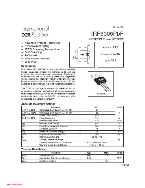
IRF5305PbFHEXFET ® Power MOSFETPD - 94788Fifth Generation HEXFETs from International Rectifier utilize advanced processing techniques to achieve extremely low on-resistance per silicon area. This benefit,combined with the fast switching speed and ruggedized device design that HEXFET Power MOSFETs are well known for, provides the designer with an extremely efficient and reliable device for use in a wide variety of applications.The TO-220 package is universally preferred for all commercial-industrial applications at power dissipation levels to approximately 50 watts. The low thermal resistance and low package cost of the TO-220 contribute to its wide acceptance throughout the industry.ParameterMax.UnitsI D @ T C = 25°C Continuous Drain Current, VGS @ -10V -31I D@ T C = 100°C Continuous Drain Current, V GS @ -10V -22A I DMPulsed Drain Current -110P D @T C = 25°C Power Dissipation 110W Linear Derating Factor 0.71W/°C V GS Gate-to-Source Voltage± 20V E AS Single Pulse Avalanche Energy 280mJ I AR Avalanche Current-16A E AR Repetitive Avalanche Energy 11mJ dv/dt Peak Diode Recovery dv/dt -5.0V/ns T J Operating Junction and-55 to + 175T STGStorage Temperature RangeSoldering Temperature, for 10 seconds 300 (1.6mm from case )°CMounting torque, 6-32 or M3 srew10 lbf•in (1.1N•m)Absolute Maximum RatingsParameterTyp.Max.UnitsR θJC Junction-to-Case––– 1.4R θCS Case-to-Sink, Flat, Greased Surface 0.50–––°C/WR θJAJunction-to-Ambient–––62Thermal ResistanceAdvanced Process Technology Dynamic dv/dt Rating175°C Operating Temperature Fast Switching P-ChannelFully Avalanche RatedLead-FreeDescription10/31/03IRF5305PbFElectrical Characteristics @ T = 25°C (unless otherwise specified)Repetitive rating; pulse width limited bymax. junction temperature. ( See fig. 11 )I SD ≤ -16A, di/dt ≤ -280A/µs, V DD ≤ V (BR)DSS ,T J ≤ 175°CNotes:V DD = -25V, starting T J = 25°C, L = 2.1mHR G = 25Ω, I AS = -16A. (See Figure 12)Pulse width ≤ 300µs; duty cycle ≤ 2%.IRF5305PbF 3Fig 4. Normalized On-ResistanceVs. TemperatureFig 2. Typical Output CharacteristicsFig 1. Typical Output Characteristics Fig 3. Typical Transfer Characteristics11010010000.1110100D DS-I , D r a i n -t o -S o u r c e C u r r e n t (A )-V , Drain-to-Source Voltage (V)11010010000.1110100D DS-I , D r a i n -t o -S o u r c e C u r r e n t (A )-V , Drain-to-Source Voltage (V)11010045678910GS-V , Gate-to-Source Voltage (V)D-I , D r a i n -t o -S o u r c e C u r r e n t (A )0.00.51.01.52.0-60-40-2020406080100120140160180JT , Junction Temperature (°C)R , D r a i n -t o -S o u r c e O n R e s i s t a n c e D S (o n)(N o r m a l i z e d )IRF5305PbFFig 8. Maximum Safe Operating AreaFig 6. Typical Gate Charge Vs.Gate-to-Source VoltageFig 5. Typical Capacitance Vs.Drain-to-Source Voltage Fig 7. Typical Source-Drain Diode Forward Voltage05001000150020002500110100C , C a p a c i t a n c e (p F )DS-V , Drain-to-Source Voltage (V)048121620102030405060Q , Total Gate Charge (nC)GG S-V , G a t e -t o -S o u r c e V o l t a g e (V )1010010000.40.81.21.62.0SD S D -I , R e v e r s e D r a i n C u r r e n t (A )-V , Source-to-Drain Voltage (V)1101001000110100DS-V , Drain-to-Source Voltage (V)D -I , D r a i n C u r r e n t (A )IRF5305PbF 5Fig 10a. Switching Time Test CircuitFig 10b. Switching Time WaveformsFig 11. Maximum Effective Transient Thermal Impedance, Junction-to-CaseFig 9. Maximum Drain Current Vs.Case TemperatureR V DDV DSVIRF5305PbF6Fig 13b. Gate Charge Test CircuitFig 13a. Basic Gate Charge WaveformFig 12c. Maximum Avalanche EnergyVs. Drain CurrentV-10VDSCurrent Sampling Resistors100200300400500600700255075100125150175JE , S i n g l e P u l s e A v a l a n c h e E n e r g y (m J )AS Starting T , Junction Temperature (°C)Fig 12b. Unclamped Inductive WaveformsFig 12a. Unclamped Inductive Test CircuitI ASV DDIRF5305PbF 7Peak Diode Recovery dv/dt Test CircuitV DD* Reverse Polarity for P-Channel** Use P-Channel Driver for P-Channel Measurements*V GS **** V GS = 5.0V for Logic Level and 3V Drive DevicesFig 14. For P-Channel HEXFETSIRF5305PbF233 Kansas St., El Segundo, California 90245, USA Tel: (310) 252-7105TAC Fax: (310) 252-7903Visit us at for sales contact information .10/03TO-220AB Package OutlineNote: For the most current drawings please refer to the IR website at:/package/分销商库存信息: IRIRF5305PBF。
- 1、下载文档前请自行甄别文档内容的完整性,平台不提供额外的编辑、内容补充、找答案等附加服务。
- 2、"仅部分预览"的文档,不可在线预览部分如存在完整性等问题,可反馈申请退款(可完整预览的文档不适用该条件!)。
- 3、如文档侵犯您的权益,请联系客服反馈,我们会尽快为您处理(人工客服工作时间:9:00-18:30)。
QX5305概述QX5305 是一款高效率,稳定可靠的高亮度LED 灯驱动控制IC ,内置高精度比较器,off-t ime 控制电路,恒流驱动控制电路等,特别适合大功率,多个高亮度LED 灯串恒流驱动。
QX5305采用固定off-t ime 控制工作方式,其工作频率可高达2.5MHz ,可使外部电感和滤波电容、体积减少,效率提高。
在DIM 脚加PWM 信号,可调节LED 灯的亮度。
通过调节外置的电阻,能控制高亮度LED 灯的驱动电流,使LED 灯亮度达到预期恒定亮度,流过高亮度LED 灯的电流可从几毫安到2安培变化。
订货信息 QX5305XP:DIP-8 LG:SO-8特性Ÿ 可编程驱动电流,最高可达2A Ÿ 高效率:最高达95%Ÿ 宽输入电压范围:5V~400V Ÿ 高工作频率:2.5MHzŸ 工作频率可调:500KHz~2.5MHz Ÿ驱动LED 灯功能强:LED 灯串可从1个到几十个LED 高亮度灯Ÿ亮度可调:通过EN 端PWM ,调节LED 灯亮度应用范围Ÿ 干电池供电LED 灯串 Ÿ LED 灯杯Ÿ RGB 大显屏高亮度LED 灯 Ÿ 平板显示器LED 背光灯 Ÿ 恒流充电器控制 Ÿ 通用恒流源方框图管脚排列图管脚定义管脚序号管脚名称功能描述1 VSS 电源地2 EN 芯片使能端3 COMP 内部比较器补偿4 FB 电压反馈端5 DRV 外部MOS驱动端6 CS 电流反馈检测脚7 TOFF 关断时间设定8 VDD 电源正(2V-6.5V)极限参数参数符号描述值单位电压Vmax VDD脚电电压8 V Vmin-max EN, CS 和FB 脚电压值-0.3-VDD+0.3 V 温度Tmin-max 工作温度范围-20-85 o C Tstorage 存储温度范围-40-165 o C ESD VESD ESD 电压(人体模式)2000 V主要电气性能和指标参数参数符号测试条件最小典型最大单位电源电压VDD 2.5 6.5 V CS 脚反馈电压V CS250 260 270 mV FB 脚反馈电压V FB250 260 270 mV 工作电流IDD 0.5 1 mA 关断时间(Toff脚悬空) T OFF0640 ns 待机电流IDDQ 1 uA EN 脚逻辑高电平V ENH 2.0 V EN脚逻辑低电平V ENL0.8 V50 nsDRV 脚电压上升时间T RISE500pF 电容在DRV 脚上时50 nsDRV脚电压下降时间T FALL500pF 电容在DRV 脚上时典型应用电路图工作原理简述QX5305 采用峰值电流检测和固定off-time控制方式。
片内的R-S触发器分别由off-time定时器置位和CS比较器、FB比较复位,它控制外部MOSFET管并和功率电感L、LED、肖特基二极管共同构成一个自振荡的,连续电感电流模式的升压型恒流LED驱动电路(参见图1)。
除了固定off-time控制这点外,QX5305的工作方式和普通的电流模式PWM控制型DC/DC升压电路非常相似。
当工作在连续电流模式下时,流过功率电感的电流I L如图2所示。
V DD上电时,off-time定时器的输出置位内部触发器使输出为高,驱动外部了功率MOSFET导通,T ON周期开始。
这时候,流过功率电感L的初始电流为零,电流以上升的模式从V IN通过功率电感L,MOSFET和电流采样电阻R CS流到地。
该电流将一部分能量储存在功率电感里并在R CS 上产生一个压降V CS。
与此同时输出滤波电容对LED放电,该电流在R FB上产生一个压降V FB,V FB被误差放大器放大。
当电流上升到使得V CS > 260mV或V FB > 误差放大器的输出电压时,CS 或FB比较器的输出复位内部触发器使得输出变低,控制外部功率MOSFET关断,T ON周期结束,T OFF周期开始。
T OFF周期内,储存在功率电感里的能量以反电势的形式与VIN叠加后,通过肖特基二极管、LED、电流反馈电阻R FB构成回路,电流呈下降的模式,与此同时输出滤波电容被充电。
当预先设置的T OFF时间间隔到达时,off-time定时器的输出再次置位内部触发器使得输出为高,外部功率MOSFET重新导通,T OFF周期结束,开始新的T ON周期,电流再次以上升的模式流通,同时输出电容对LED放电……。
依次循环往复,使LED上的电流得以连续而且保持稳定。
正常工作情况下,电感电流上升、下降的斜率与V IN、功率电感L的感值和LED的正向压降相关。
V CS间接反映了电感的峰值电流,也代表了峰值功率,而V FB间接反映了输出电流的大小。
QX5305根据V FB来不断调节外部功率MOSFET管导通的时间T ON,即输出电流的脉冲宽度(也就是输入到功率电感L中的能量增加,导致流过负载的输出电流变大,反之则反。
如此闭环调节使得输出电流能够得到恒定。
应用指引1)L ED 电流的设定LED的电流由R FB设定,R F B阻值不同,就可以设置不同的LED驱动电流。
R F B 的估算公式如下:R F B=260mV/I OI O为驱动LED灯的电流。
2)峰值功率的限定限定峰值功率可以减小上电时的冲击电流,并且在电路异常时可以起到保护作用。
峰值功率由R C S设定,R C S的计算公式如下:R C S=260mV/Io*K K=0.7*V I N/V O也即:R C S=R FB*0.7*V I N/V OI O为驱动LED灯的电流;V O为输出电压,即所有串联LED正向电压的总和。
3)工作频率的确定QX5305采用固定o ff-t ime控制工作方式,其工作频率为F=1/(T O F F+T O N)其中T O N时间与功率电感的感值和输入输出的电压差相关,而T O FF的off-t ime 时间由片内的off-t ime 定时器和片外的T O F F管脚的R O FF、C O F F决定。
因此可通过外部电阻和电容设置最小T O F F时间,从而间接设定工作频率,其中点空比约为D≈(V O UT-V I N)/V O UT,而T O F F计算公式如下:这里100KΩ电阻和12pF电容是芯片内部集成的参数,当T OF F管脚悬空时:在T O FF管脚上单独接R O F F电阻可以提搞工作频率,而单独接C O FF则可以降低工作频率。
例如:当T O FF脚接470pF电容时,T O F F≈24.6uS,如果D=0.1,则电路工作频率F约为36.6KHz。
工作频率的高低,是要根据实际使用情况来决定的。
工作频率高,功率电感的数值可以越小,电感的体积也越小,同时也有利于选用低容值小体积的输入输出滤波电容。
但是较高的工作频率会导致MOSFET管和肖特基二极管的开关损耗增加,发热加剧,导致电路的效率下降。
这点在高输出电压下工作时较为明显。
因此,如果在高于80V的工作条件下,建议QX5305的工作频率不宜超过80KHz。
4)功率电感L选择功率电感L的选用原则,一是确保流过LED的电流是连续的并且纹波电流ΔI 值远小于流过LED的电流值,其次是保证其工作时不会出现磁饱和现象。
QX5305电路在工作时,输入电源在MOSFET管导通T O N期间直接对功率电感提供能量,其于时间则由电源与功率电感内储存的能量来维持LED电流。
换句话说,功率电感在MOSFET管导通时储能,MOSFET管关闭时释放能量,电感及LED上的电流方向始终是不变的。
功率电感的充放电在输出电流上形成锯齿状纹波电流(见图2)。
纹波电流(ΔI=I M A X-I LI N)的上升下降斜率及幅值直接与电感上的电压和电感量相关,其关系如下式:T O N时:V L=V I N-V D P-V C S;T O F F时:V L=-V I N+LED+V F纹波电流ΔI的大小与功率电感的电感量成反比例,当纹波电流过大时,将导致输出电流的断续(此时可以理解为:T O N时功率电感内储存的能量不足以在T O F F 时释放来维持负载电流)。
因而,一定的工作电压、负载下,不同的电感元件参数,流过负载的电流会出现连续模式和非连续两种模式。
在驱动LED的情况下,为保持LED电流的恒定,不希望出现非连续模式。
因此,在工作电压、负载一定的情况下,必须合理地选择功率电感数值以保证电路工作于连续模式下。
当功率电感的电感量足够大时,一般可保证电流不会出现非连续模式。
同时较大的电感量也使得流过负载的电流脉动分量较小,有利于延长LED的寿命。
通常可根据以下公式估算出保证连续模式工作的最小电感量,然后在条件许可的情况下,尽可能地采用较大的电感量值。
在off-t ime期,流过LED灯的ΔI L计算如下:为了使流过LED灯电流波动小于ΔI L,电感值应满足:T O F F在上一节中由R O F F和C O F F来设定,ΔI L可取I L的十分之一。
通常,当输入、输出电压的压差较大或者输出功率较大时,需要加大功率电感的值,反之,可以用较小的功率电感值。
一般取值约在几百微亨到十几毫亨,视实际应用而定。
另外不可忽视的一个问题是,QX5305工作时流过功率电感的峰值电流通常可高达安培级以上,所选用的功率电感必须具有足够的DC 工作电流容量,否则电感会发生磁饱和,造成电路的效率大大下降,甚至电路不能正常稳定工作。
一般情况下,要求功率电感的饱和电流必须大于最大输出电流的 1.5倍以上。
同时在大电流条件下功率电感本身的内阻(ESR)也不可忽视,它会极大地影响转换效率。
所以,在确定了电感量以后,如果希望提高QX5305驱动器的工作效率,在体积允许的情况下,可选用较大的磁性元件及较粗的导线绕制的功率电感。
5)MOSFET 管的选用首先要考虑MOSFET的耐压,一般要求MOSFET的耐压高于最大输出的电压 1.5倍以上。
其次,根据驱动LED灯电流的大小,选择MOSFET的I最大电流。
一般情D S最大电流是LED灯驱动电流的3倍以上。
另外MOSFET 况下,应选用MOSFET的ID S越小,在MOSFET管上面的功率越小,电路的工作效率就越的内阻要尽可能小;RD S高。
另外,高电压应用时,由于高耐压的MOSFET管完全导通所需的驱动电压V G S也比较高(可能会高于QX5305的输出驱动电平),为此应该选择V G S低于5V的型号。
6)EN使能端在EN端接(低电平)地时,QX5305处于休眠状态,此时,工作电流小于10uA,自耗电非常小,当EN端为高电平时,QX5305处于工作状态,此时空载工作电流约为200uA。
7)LED灯亮度调节LED灯的亮度调节,可由以下二种方法:第一种方法是模拟调光,通过改变R FB的电阻。