阿莫电子论坛
IV电路分析

不错 看地电路挺精妙的。学些了
2011-02-25,09:29:34
资料 邮件 回复 引用回复 ↑↑ ↓↓
编辑 删除
广告投诉、提议置酷等 提交
【21楼】 dszx 积分:141 派别: 等级:-----来自:新疆石河子市
LZ:0-5V转换0-20mA,0mA能实现吗?MC1458能做的0mA后小数点几位?我用OP2177做过,可实现0.004mA的零位。
编辑 删除
广告投诉、提议置酷等 提交
积分:501 派别: 等级:-----来自:
/bbs/bbs_content.js…
(原文件名:VI变换电路分析vol2_Page_2.jpg) 引用图片
11/21
2011-4-14
0-5V转换-20mA V/I电路分析 中国电…
2011-02-27,15::27
积分:1211
派别:
等级:------
来自:
2011-02-25,09:13:36
资料 邮件 回复 引用回复 ↑↑ ↓↓
【18楼】 USACH 美丽 坚和中国 积分:259 派别: 等级:-----来自:
我这两天也一直在研究这个,唉,谢谢。
__________________________ 美丽坚和中国。
/bbs/bbs_content.js…
(原文件名:VI变换电路分析vol2_Page_7.jpg) 引用图片
18/21
2011-4-14
2011-02-27,15:23:57
0-5V转换-20mA V/I电路分析 中国电…
资料 邮件 回复 引用回复 ↑↑ ↓↓
编辑 删除
╟—虚拟总论坛
跳转至:
↓↓ 0-5V转换-20mA V/I电路分析
兄弟MFC-8460N_8860DN_DCP-8060维修手册

USB-6009用户使用手册
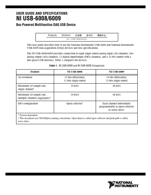
USER GUIDE AND SPECIFICATIONSNI USB-6008/6009Bus-Powered Multifunction DAQ USB DeviceThis user guide describes how to use the National Instruments USB-6008 and National Instruments USB-6009 data acquisition (DAQ) devices and lists specifications.The NI USB-6008/6009 provides connection to eight single-ended analog input (AI) channels, two analog output (AO) channels, 12 digital input/output (DIO) channels, and a 32-bit counter with afull-speed USB interface. Table1 compares the devices.Table 1. NI USB-6008 and NI USB-6009 ComparisonFeature NI USB-6008NI USB-6009AI resolution12 bits differential,11 bits single-ended 14 bits differential, 13 bits single-endedMaximum AI sample rate, single channel*10 kS/s48 kS/s Maximum AI sample rate,multiple channels (aggregate)*10 kS/s48 kS/sDIO configuration Open collector†Each channel individuallyprogrammable as open collectoror active drive†* System-dependent.† This document uses NI-DAQmx naming conventions. Open-drain is called open collector and push-pull is called active drive.Figure1 shows key functional components of the NI USB-6008/6009.Figure 1. NI USB-6008/6009 Block DiagramContentsSafety Guidelines (3)Electromagnetic Compatibility Guidelines (3)Unpacking (4)Setting Up the NI USB-6008/6009 (4)Using the NI USB-6008/6009 in an Application (6)Features (7)USB Connector and USB Cable Strain Relief (7)LED Indicator (8)Screw Terminal Connector Plugs (8)Firmware (8)Cables and Accessories (9)Pinout and Signal Descriptions (9)NI USB-6008/6009 User Guide and © National Instruments Corporation 3NI USB-6008/6009 User Guide and SpecificationsAnalog Input (11)Analog Input Modes and Signal Sources (11)Floating Signal Sources.......................................................................................................12Ground-Referenced Signal Sources.....................................................................................13Taking Differential Measurements......................................................................................14Taking Referenced Single-Ended Measurements................................................................15Digital Trigger.............................................................................................................................15Analog Output.. (16)Connecting Analog Output Loads...............................................................................................16Minimizing Glitches on the Output Signal..................................................................................16Digital I/O.. (17)Source/Sink Information..............................................................................................................18I/O Protection...............................................................................................................................19Power-On States..........................................................................................................................19Static DIO....................................................................................................................................19PFI 0.. (19)Using PFI 0 as a Digital Trigger..................................................................................................19Using PFI 0 as an Event Counter.................................................................................................19External Reference and Power Source. (20)+2.5V External Reference...........................................................................................................20+5 V Power Source......................................................................................................................20Specifications.......................................................................................................................................20Where to Go from Here.. (27)Example Programs.......................................................................................................................27Related Documentation................................................................................................................27Where to Go for Support (30)Safety GuidelinesOperate the NI USB-6008/6009 device only as described in this user guide.CautionDo not operate the NI USB-6008/6009 in a manner not specified in this document. Misuseof the device can result in a hazard. You can compromise the safety protection built into the device if the device is damaged in any way. If the device is damaged, contact National Instruments for repair.CautionDo not substitute parts or modify the device except as described in this document. Use thedevice only with the chassis, modules, accessories, and cables specified in the installation instructions. You must have all covers and filler panels installed during operation of the device.CautionDo not operate the device in an explosive atmosphere or where there may be flammablegases or fumes. If you must operate the device in such an environment, it must be in a suitably rated enclosure.Electromagnetic Compatibility GuidelinesThis product was tested and complies with the regulatory requirements and limits for electromagnetic compatibility (EMC) as stated in the product specifications. These requirements and limits are designed to provide reasonable protection against harmful interference when the product is operated in its intended operational electromagnetic environment.This product is intended for use in industrial locations. There is no guarantee that harmful interference will not occur in a particular installation, when the product is connected to a test object, or if the productis used in residential areas. To minimize the potential for the product to cause interference to radio andNI USB-6008/6009 User Guide and Specifications television reception or to experience unacceptable performance degradation, install and use this product in strict accordance with the instructions in the product documentation.Furthermore, any changes or modifications to the product not expressly approved by National Instruments could void your authority to operate it under your local regulatory rules.Caution To ensure the specified EMC performance, operate this product only with shielded cablesand accessories.Caution This product may become more sensitive to electromagnetic disturbances in the operationalenvironment when test leads are attached or when connected to a test object.Caution Emissions that exceed the regulatory requirements may occur when this product isconnected to a test object.CautionChanges or modifications not expressly approved by National Instruments could void theuser’s authority to operate the hardware under the local regulatory rules.UnpackingThe NI USB-6008/6009 device ships in an antistatic package to prevent electrostatic discharge (ESD). ESD can damage several components on the device.CautionNever touch the exposed pins of connectors.To avoid ESD damage in handling the device, take the following precautions:•Ground yourself with a grounding strap or by touching a grounded object.•Touch the antistatic package to a metal part of your computer chassis before removing the device from the package.Remove the device from the package and inspect it for loose components or any other signs of damage. Notify NI if the device appears damaged in any way. Do not install a damaged device in your computer or chassis.Store the device in the antistatic package when the device is not in use.Setting Up the NI USB-6008/6009Complete the following steps to get started with the NI USB-6008/6009.NoteFor information about non-Windows operating system support, refer to the Getting Started with NI-DAQmx Base for Linux and Mac OS X Users document available from /manual s .1.Install the application software (if applicable), as described in the installation instructions that accompany your software.2.Install NI-DAQmx 1.NoteThe NI-DAQmx software is included on the disk shipped with your kit and is available for download at /s upport . The documentation for NI-DAQmx is available after installation from Start»All Programs»National Instruments»NI-DAQ . Other NI documentation is available from /manual s .1NI USB-6008/6009 devices are supported by NI-DAQmx 7.5 and later.© National Instruments Corporation 5NI USB-6008/6009 User Guide and Specifications3.Install the 16-position screw terminal connector plugs by inserting them into the connector jacks as shown in Figure 2.Figure 2. Signal Label Application Diagram4.Affix the provided signal labels to the screw terminal connector plugs. You can choose labels with pin numbers, signal names, or blank labels, as shown in Figure 3. Choose one of the labels, align the correct label with the terminals printed on the top panel of your device and apply the label, as shown in Figure 2.Figure 3. NI USB-6008/6009 Signal LabelsNoteAfter you label the screw terminal connector plugs, you must only insert them into the matching connector jack, as indicated by the overlay label on the device.5.Plug one end of the USB cable into the NI USB-6008/6009 and the other end into an available USB port on the computer.1Overl a y L ab el with Pin Orient a tion G u ide s 2S crew Termin a l Connector Pl u g3S ign a l L ab el 4U S B C ab le1U s er-Defined C us tom L ab el 2Termin a l N u m b er L ab el 3Digit a l I/O L ab el4An a log Inp u t Differenti a l S ign a l N a me L ab el 5An a log Inp u t S ingle-Ended S ign a l N a me L abelNI USB-6008/6009 User Guide and Specifications 6.Double-click the Measurement & Automation icon, shown at left, on the desktop to open Measurement & Automation Explorer (MAX).7.Expand My System»Devices and Interfaces and verify that the NI USB-6008/6009 is listed. If your device does not appear, press <F5> to refresh the view in MAX. If your device is still not recognized, refer to /s upport/daqmx for troubleshooting information.8.Self-test your device in MAX by right-clicking NI USB-600x and selecting Self-Test . Self-test performs a brief test to determine successful device installation. When the self-test finishes, a message indicates successful verification or if an error occurred. If an error occurs, refer to /s upport/daqmx .CautionTo ensure the specified EMC performance, operate this product only with shielded cablesand accessories.9.Connect the wires (16 to 28 AWG) of a shielded, multiconductor cable to the screw terminals by stripping 6.35 mm (0.25 in.) of insulation, inserting the wires into the screw terminals, and securely tightening the screws with the flathead screwdriver to a torque of 0.22–0.25 N · m (2.0–2.2lb · in.). Refer to Figure 6 for the NI USB-6008/6009 pinout.If using a shielded cable, connect the cable shield to a nearby GND terminal.NoteFor information about sensors, go to /s en s or s . For information about IEEE 1451.4 TEDS smart sensors, go to /ted s .10.Run a Test Panel in MAX by right-clicking NI USB-600x and selecting Test Panels .Click Start to test the device functions, or Help for operating instructions. Click Close to exit the test panel.Using the NI USB-6008/6009 in an ApplicationYou can use the DAQ Assistant through many NI application software programs to configure virtual and measurement channels. Table 2 lists DAQ Assistant tutorial locations for NI applications.Refer to the Where to Go from Here section for information about programming examples for NI-DAQmx and NI-DAQmx Base.Table 2. DAQ Assistant Tutorial LocationsNI Application Tutorial LocationLabVIEWGo toHelp»LabVIEW Help . Next, go to Getting Started with LabVIEW»Getting Started with DAQ»Taking an NI-DAQmx Measurement in LabVIEW .LabWindows ™/CVI ™Go to Help»Contents . Next, go to Using LabWindows/CVI»Data Acquisition»Taking an NI-DAQmx Measurement in LabWindows/CVI .Measurement StudioGo to NI Measurement Studio Help»Getting Started with the MeasurementStudio Class Libraries»Measurement Studio Walkthroughs»Walkthrough: Creating a Measurement Studio NI-DAQmx Application .LabVIEW SignalExpressGo to Help»Taking an NI-DAQmx Measurement in SignalExpress .© National Instruments Corporation 7NI USB-6008/6009 User Guide and SpecificationsFeaturesThe NI USB-6008/6009 features a USB connector, USB cable strain relief, two screw terminal connector plugs for I/O, and an LED indicator, as shown in Figure 4.Figure 4. NI USB-6008/6009 Top and Back ViewsUSB Connector and USB Cable Strain ReliefThe NI USB-6008/6009 features a USB connector for full-speed USB interface. You can provide strain relief for the USB cable by threading a zip tie through the USB cable strain relief ring and tightening around a looped USB cable, as shown in Figure 5.Figure 5. NI USB-6008/6009 Strain Relief1U S B C ab le S tr a in Relief2S crew Termin a l Connector Pl u g3LED Indic a tor 4U S B ConnectorLED IndicatorThe NI USB-6008/6009 device has a green LED indicator that indicates device status, as listed inTable3. When the device is connected to a USB port, the LED blinks steadily to indicate that the device is initialized and is receiving power from the connection.Table 3. LED State/Device StatusLED State Device StatusNot lit Device not connected or in suspendOn, not blinking Device connected but not initialized, or the computer is in standby mode.In order for the device to be recognized, the device must be connected to a computer thathas NI-DAQmx installed on it.Single-blink Operating normallyScrew Terminal Connector PlugsThe NI USB-6008/6009 ships with one detachable screw terminal connector plug for analog signals and one detachable screw terminal connector plug for digital signals. These screw terminal connectorsprovide 16 connections that use 16–28AWG wire. Refer to step4 of the Setting Up theNI USB-6008/6009 section for information about selecting labels for the screw terminal connectorplugs. Refer to the Pinout and Signal Descriptions section for the device pinout and signal descriptions.You can order additional connectors and labels for your device. Refer to the Cables and Accessoriessection for ordering information.FirmwareThe firmware on the NI USB-6008/6009 refreshes whenever the device is connected to a computer with NI-DAQmx. NI-DAQmx automatically uploads the compatible firmware version to the device. Thefirmware version may be upgraded when new versions of NI-DAQmx release.NI USB-6008/6009 User Guide and © National Instruments Corporation 9NI USB-6008/6009 User Guide and SpecificationsCables and AccessoriesTable 4 contains information about cables and accessories available for the NI USB-6008/6009. For a complete list of accessories and ordering information, refer to the pricing section of the NI USB-6008 or NI USB-6009 product page at .Pinout and Signal DescriptionsFigure 6 shows the pinout of the NI USB-6008/6009. Analog input signal names are listed assingle-ended analog input name, AI x , and then differential analog input name, (AI x +/–). Refer to Table 5 for a detailed description of each signal.Figure 6. NI USB-6008/6009 PinoutTable 4. NI USB-6008/6009 Cables and AccessoriesAccessoryPart Number DescriptionUSB-6008/6009 Accessory Kit 779371-01Four additional screw-terminal connectors, connector labels, and a screwdriverUSB-6000 Series Prototyping Accessory779511-01Unshielded breadboarding accessory forcustom-defined signal conditioning and prototyping. You can use up to two accessories per device.Hi-Speed USB Cable184125-01184125-021 m and2 m lengthsCaution : For compliance with Electromagnetic Compatibility (EMC) requirements, this product must be operated with shielded cables and accessories. If unshielded cables or accessories are used, the EMC specifications are no longerguaranteed unless all unshielded cables and/or accessories are installed in a shielded enclosure with properly designed and shielded input/output ports.Table 5. Signal DescriptionsSignal Name Reference Direction DescriptionGND——Ground—The reference point for the single-ended analog inputmeasurements, analog output voltages, digital signals, +5VDC supply,and +2.5VDC at the I/O connector, and the bias current return point fordifferential mode measurements.AI <0..7>Varies Input Analog Input Channels 0 to 7—For single-ended measurements, eachsignal is an analog input voltage channel. For differential measurements,AI0and AI4 are the positive and negative inputs of differential analoginput channel 0. The following signal pairs also form differential inputchannels: AI<1, 5>, AI<2, 6>, and AI<3, 7>. Refer to the Analog Inputsection for more information.AO <0, 1>GND Output Analog Output Channels 0 and 1—Supplies the voltage output ofAO channel0 or AO channel 1. Refer to the Analog Output section formore information.P0.<0..7>GND Input or Output Port0 Digital I/O Channels0to7—You can individually configureeach signal as an input or output. Refer to the Digital I/O section formore information.P1.<0..3>GND Input or Output Port1 Digital I/O Channels0to3—You can individually configureeach signal as an input or output. Refer to the Digital I/O section for moreinformation.PFI 0GND Input PFI 0—This pin is configurable as either a digital trigger or an eventcounter input. Refer to the PFI0 section for more information.+2.5 V GND Output+2.5 V External Reference—Provides a reference for wrap-backtesting. Refer to the +2.5V External Reference section for moreinformation.+5 V GND Output+5 V Power Source—Provides +5V power up to 200mA. Refer to the+5 V Power Source section for more information.NI USB-6008/6009 User Guide and Analog InputThe NI USB-6008/6009 has eight analog input channels that you can use for four differential analoginput measurements or eight single-ended analog input measurements.Figure7 shows the analog input circuitry of the NI USB-6008/6009.Figure 7. NI USB-6008/6009 Analog Input CircuitryThe main blocks featured in the NI USB-6008/6009 analog input circuitry are as follows:•MUX—The NI USB-6008/6009 has one analog-to-digital converter (ADC). The multiplexer (MUX) routes one AI channel at a time to the PGA.•PGA—The progammable-gain amplifier provides input gains of 1, 2, 4, 5, 8, 10, 16, or 20 when configured for differential measurements and gain of 1 when configured for single-endedmeasurements. The PGA gain is automatically calculated based on the voltage range selected in themeasurement application.•ADC—The analog-to-digital converter (ADC) digitizes the AI signal by converting the analog voltage into digital code.•AI FIFO—The NI USB-6008/6009 can perform both single and multiple analog-to-digital conversions of a fixed or infinite number of samples. A first-in-first-out (FIFO) buffer holds dataduring AI acquisitions to ensure that no data is lost.Analog Input Modes and Signal SourcesYou can configure the AI channels on the NI USB-6008/6009 to take differential or referencedsingle-ended (RSE) measurements. Table6 summarizes the recommended analog input mode(s) forfloating signal sources and ground-referenced signal sources. Refer to Table5 for more informationabout I/O connections for single-ended or differential measurements.Table 6. Analog Input ConfigurationsFloating Signal SourcesA floating signal source is not connected to the building ground system, but has an isolatedground-reference point. Some examples of floating signal sources are outputs of transformers, thermocouples, battery-powered devices, optical isolators, and isolation amplifiers. An instrument or device that has an isolated output is a floating signal source.Refer to the NI Developer Zone document, Field Wiring and Noise Considerations for Analog Signals, for more information. To access this document, go to /info and enter the Info Code rdfwn3. When to Use Differential Connections with Floating Signal SourcesUse DIFF input connections for any channel that meets any of the following conditions:•Your application requires input ranges other than ±10 V.•The input signal is low level and requires greater accuracy.•The leads connecting the signal to the device are greater than 3m (10ft).•The input signal requires a separate ground-reference point or return signal.•The signal leads travel through noisy environments.•Two analog input channels, AI+ and AI–, are available for the signal.DIFF signal connections reduce noise pickup and increase common-mode noise rejection. DIFF signal connections also allow input signals to float within the working voltage of the device.Refer to the Taking Differential Measurements section for more information about differential connections.When to Use Referenced Single-Ended (RSE) Connections with Floating Signal SourcesOnly use RSE input connections if the input signal meets all of the following conditions:•The input signal can share a common reference point, GND, with other signals that use RSE.•Your application permits the use of the ±10 V input range.•The leads connecting the signal to the device are less than 3m (10ft).DIFF input connections are recommended for greater signal integrity for any input signal that does not meet the preceding conditions.In the single-ended modes, more electrostatic and magnetic noise couples into the signal connections than in DIFF configurations. The coupling is the result of differences in the signal path. Magnetic coupling is proportional to the area between the two signal conductors. Electrical coupling is a function of how much the electric field differs between the two conductors.With this type of connection, the PGA rejects both the common-mode noise in the signal and the ground potential difference between the signal source and the device ground.Refer to the Taking Referenced Single-Ended Measurements section for more information about RSE connections.Ground-Referenced Signal SourcesA ground-referenced signal source is a signal source connected to the building system ground. It is already connected to a common ground point with respect to the device, assuming that the computer is plugged into the same power system as the source. Non-isolated outputs of instruments and devices that plug into the building power system fall into this category.The difference in ground potential between two instruments connected to the same building power system is typically between 1 and 100 mV, but the difference can be much higher if power distribution circuits are improperly connected. If a grounded signal source is incorrectly measured, this difference can appear as measurement error. Follow the connection instructions for grounded signal sources to eliminate this ground potential difference from the measured signal.Refer to the NI Developer Zone document, Field Wiring and Noise Considerations for Analog Signals, for more information. To access this document, go to /info and enter the Info Code rdfwn3. When to Use Differential Connections with Ground-Referenced Signal SourcesUse DIFF input connections for any channel that meets any of the following conditions:•Your application requires input ranges other than ±10 V.•The input signal is low level and requires greater accuracy.•The leads connecting the signal to the device are greater than 3m (10ft).•The input signal requires a separate ground-reference point or return signal.•The signal leads travel through noisy environments.•Two analog input channels, AI+ and AI–, are available for the signal.DIFF signal connections reduce noise pickup and increase common-mode noise rejection. DIFF signal connections also allow input signals to float within the working voltage of the device.Refer to the Taking Differential Measurements section for more information about differential connections.When to Use Referenced Single-Ended (RSE) Connections with Ground-Referenced Signal Sources Do not use RSE connections with ground-referenced signal sources. Use differential connections instead.As shown in the bottom-rightmost cell of Table6, there can be a potential difference between GND and the ground of the sensor. In RSE mode, this ground loop causes measurement errors.Taking Differential MeasurementsFor differential signals, connect the positive lead of the signal to the AI+terminal, and the negative lead to the AI– terminal.Figure 8. Connecting a Differential Voltage SignalThe differential input mode can measure ±20 V signals in the ±20V range. However, the maximum voltage on any one pin is ±10 V with respect to GND. For example, if AI 1 is +10 V and AI 5 is –10 V, then the measurement returned from the device is +20 V.Figure 9. Example of a Differential 20 V MeasurementConnecting a signal greater than ±10 V on either pin results in a clipped output.Figure 10. Exceeding ±10 V on AI Returns Clipped OutputTaking Referenced Single-Ended MeasurementsTo connect referenced single-ended (RSE) voltage signals to the NI USB-6008/6009, connect thepositive voltage signal to an AI terminal, and the ground signal to a GND terminal, as shown inFigure11.Figure 11. Connecting a Referenced Single-Ended Voltage SignalWhen no signals are connected to the analog input terminal, the internal resistor divider may cause the terminal to float to approximately 1.4 V when the analog input terminal is configured as RSE. Thisbehavior is normal and does not affect the measurement when a signal is connected.Digital TriggerYou can configure PFI0 as a digital trigger input for analog input tasks. Refer to the Using PFI0 as a Digital Trigger section for more information.Analog OutputThe NI USB-6008/6009 has two independent analog output channels that can generate outputs from 0 to 5 V. All updates of analog output channels are software-timed. GND is the ground-reference signal for the analog output channels.Figure12 shows the circuitry of one analog output channel on the NI USB-6008/6009.Figure 12. Circuitry of One Analog Output ChannelThe main block featured in the NI USB-6008/6009 analog output circuitry is the digital-to-analogconverter (DAC), which converts digital codes to analog voltages. There is one DAC for each analogoutput line.Connecting Analog Output LoadsTo connect loads to the NI USB-6008/6009, connect the positive lead of the load to the AO terminal,and connect the ground of the load to a GND terminal, as shown in Figure13.Figure 13. Connecting a LoadMinimizing Glitches on the Output SignalWhen you use a DAC to generate a waveform, you may observe glitches in the output signal. Theseglitches are normal; when a DAC switches from one voltage to another, it produces glitches due toreleased charges. The largest glitches occur when the most significant bit of the DAC code changes. You can build a lowpass deglitching filter to remove some of these glitches, depending on the frequency and nature of the output signal. For more information about minimizing glitches. refer to theKnowledgeBase document, Reducing Glitches on the Analog Output of MIO DAQ Devices. To access this document, go to /info and enter the Info Code ex s zek.。
gerber file(文件)说明介绍

G E R B E R F I L E 简介
常见数字和字母意义 D01 LIGHT ON D02 LIGHT OFF D03 FLASH D10 Dn APETURE CODE G54 更换镜头 M02 结束
M02 R S - 2 7 4 - X 格式 EX %FSLAX24Y24*% INCH %IPPOS*%%MO IN *% %AMETCH100V* 22 1 0.075000 0.075000 -0.000700 -0.000700 -45.000000* 22 1 0.075000 0.075000 0.000000 0.000000 135.000000* % %ADD10C 0.01500*% %ADD11C 0.01000*% %ADD12C 0.01400*% %ADD13C 0.02500*% %ADD14C 0.05000*% %ADD15C 0.07500*% %ADD17C 0.06600*% %ADD24C 0.08000*% %ADD25C 0.17500*% %ADD26C 0.09000*% %ADD27C 0.10000*% %ADD28C 0.06000*% %LNE115.GTL*% %LPD*% -------作线
ANNULUS
TARGET
THERMAL 花孔
使用者自定义镜头 CUSTOMER APETURE
常见镜头档格式 见 C \CONVERT 目录下的 DOC 文件
X149.19Y62.01M50 X149.2Y-.04M50M30 X10.Y-7.5M30 X16.01Y3.3T04M31 X61.67Y3.28 X76.95Y3.28 XYM50 X.01Y62.M50 X.03Y124.07M50 X.04Y186.09M50 X149.18Y186.07M50 X149.21Y124.04M50 X149.19Y62.01M50 X149.2Y-.04M50M30 X20.Y-7.5M30 E x e l . d r l 格式 EX % M48 T1C0.125 T2C0.028 T3C0.035 T4C0.0394 T5C0.04 T6C0.0433 % T1 X0Y114222 X0025Y114222 X06417Y114722 X12584Y114222 X12834Y114222 X12834Y-002 X12584Y-002 X06417Y-0025 X005Y-002 X0025Y-002 X0Y-002 T2 X0311Y00788 X03425Y00788
关于8051 bootloader的一个思路 (amoBBS 阿莫电子论坛)

关于8051 bootloader的一个思路(amoBBS 阿莫电子论坛)前一段时间做了个8051的bootloader,在C8051F340上运行,效果还可以。
基本思路如下:1,中断向量的处理。
考虑到应用的可靠性,bootloader不应被擦除,而bootloader 和中断向量表通常都在单片机程序区的起始位置,所以中断向量表也不能变。
有些bootloader的解决方法是对主程序里的所有中断函数定位,这样做很麻烦。
我的解决的办法是,在startup.a51里,添加这样的语句org 0003Hljmp 3000Horg ....ljmp .....0003H是第一个中断的入口,而3000H是主程序里的地址,在这里用一系列org、ljmp的语句全部跳到3000H 开始的连续位置。
在主程序的工程属性里,option for target->C51,Interrupt vectors at设置里,设置为0x3000。
这样,编译器就会把中断入口函数定位在3000H开始的位置。
唯一的缺点只是所有的中断会延迟一个ljmp指令的执行周期。
这样做,主程序里就不必对中断函数做特别的处理。
2,bootloader的处理流程:首先,bootloader检查主程序是否正常。
主程序在下载的时候,会提供一个校验码,这个校验码也会保存在一个特定位置,如果发现校验码出错,则提示并进入下载模式然后,bootloader检查有没有用户要求升级的(这个请求可以来自任何通讯接口),如果有,则进入升级模式。
如果主程序没有错误,在一定时间内也没有用户要求升级的请求,则进入主程序开始运行。
因为前面提到,中断向量表已经做了重映射,所以bootloader 里一般不使用中断。
3,主程序的处理主程序除了第一点提到的,要对中断向量做一个重定位,还需要对入口定位,以确保bootloader顺利进入主程序。
另外,主程序需要在工程属性里设置ROM地址范围,当然,那个重映射的中断向量表,肯定要在这个范围内。
CodeWarrior使用说明
htt第p:/一/bb章s.el认ecf识oomd电eW子技a术rr论io坛r 电子发烧上友海天马
5.5.4).隐藏文件夹(Shielded Folders): 在这里指定的文件夹在工程设计期间,或 执行查找和比较操作期间,将要被忽略掉.如果在你的工程级有一个巨大的“数据”文 件目录,而你又不想让这些文件降低CodeWarrior 的操作速度时,这个设置就很管用 了;
5.3.2).视窗化(Windowing): 设定调试器如何管理它的窗口(比如隐藏所有打开 的编辑器窗口);
htt第p:/一/bb章s.el认ecf识oomd电eW子技a源自rr论io坛r 电子发烧上友海天马
5.3.3).全局设置(Global Settings): 几个用于定制调试器在全局层次如何工作 的设置。比如当一个包含了程序调试信息的文件被打开时,是否启动这个程序;
的使用的设置。正如你所见到的,CodeWarrior 有许多设置项和选项。设置完后点 击“Save”按钮保存你所作的修改,点击“Close”按钮将忽略你所作的所有修改。在进 入下一节课之前,多练习几次。最后请确认“默认的文本文件格式(Default Text File Format)”(在编辑器设置面板中)保持为 DOS 设置。
htt第p:/一/bb章s.el认ecf识oomd电eW子技a术rr论io坛r 电子发烧上友海天马
1). CodeWarrior 能做些什么? A).使用 C/C++ 进行编程 B).也支持 Java 开发 本课程仅限于应用C/C++ 语言在 Windows 平台上使用 CodeWarrior 进行的开发. 2). CodeWarrior 优点是什么? CodeWarrior 能够自动地检查代码中的明显错误,它通过一个集成的调试器和编辑器来扫描
总结 fpga难学 的几大原因 (amobbs 阿莫电子论坛)
总结FPGA难学的几大原因(转)(amoBBS 阿莫电子论坛)为什么很多菜鸟始终无法入门?为什么大量的人会觉得FPGA难学?开贴来详细讲一下菜鸟觉得FPGA难学的几大原因:1、不熟悉FPGA的内部结构,不了解可编程逻辑器件的基本原理。
FPGA为什么是可以编程的?恐怕很多菜鸟不知道,他们也不想知道。
因为他们觉得这是无关紧要的。
他们潜意识的认为可编程嘛,肯定就是像写软件一样啦。
软件编程的思想根深蒂固,看到Verilog或者VHDL就像看到C语言或者其它软件编程语言一样。
一条条的读,一条条的分析。
如果这些菜鸟们始终拒绝去了解为什么FPGA是可以编程的,不去了解FPGA的内部结构,要想学会FPGA 恐怕是天方夜谭。
虽然现在EDA软件已经非常先进,像写软件那样照猫画虎也能综合出点东西,但也许只有天知道EDA软件最后综合出来的到底是什么。
也许点个灯,跑个马还行。
这样就是为什么很多菜鸟学了N久以后依然是一个菜鸟的原因。
那么FPGA为什么是可以“编程”的呢?首先来了解一下什么叫“程”。
启示“程”只不过是一堆具有一定含义的01编码而已。
编程,其实就是编写这些01编码。
只不过我们现在有了很多开发工具运算或者是其它操作。
所以软件是一条一条的,通常都不是直接编写这些01编码,而是以高级语言的形式来编写,最后由开发工具转换为这种01编码而已。
对于软件编程而言,处理器会有一个专门的译码电路逐条把这些01编码翻译为各种控制信号,然后控制其内部的电路完成一个个的读,因为软件的操作是一步一步完成的。
而FPGA的可编程,本质也是依靠这些01编码实现其功能的改变,但不同的是FPGA之所以可以完成不同的功能,不是依靠像软件那样将01编码翻译出来再去控制一个运算电路,FPGA里面没有这些东西。
FPGA内部主要三块:可编程的逻辑单元、可编程的连线和可编程的IO模块。
可编程的逻辑单元是什么?其基本结构某种存储器(SRAM、FLASH等)制成的4输入或6输入1输出地“真值表”加上一个D触发器构成。
RefMan_mmslite(前30页)
COPYRIGHT NOTICE
© Copyright 1994 - 2008 Systems Integration Specialists Company Inc., All Rights Reserved. This document is provided under license to authorized licensees only. No part of this document may be copied or distributed, transmitted, transcribed, stored in a retrieval system, or translated into any human or computer language, in any form or by any means, electronic, mechanical, magnetic, manual, or otherwise, disclosed to third parties, except as allowed in the license agreement, without the express written consent of Systems Integration Specialists Company Incorporated, 6605 19½ Mile Road, Sterling Heights, MI, 48314, U.S.A.
Tel: +586-254-0020, Fax: +586-254-0053 E-Mail: support@, URL: http:\\
Printed in U.S.A.
07/2008
DWG#100275/2.4
把Lua移植到stm32上,效果不错!(amoBBS阿莫电子论坛)
把Lua移植到stm32上,效果不错!(amoBBS阿莫电子论坛)因为我们产品的需要满足不同行业需求,所以一直在寻找一个脚本语言,以便灵活配置。
前段时间还自己花时间去实现一个C语言解释器,看了一堆编译原理的东西,以及虚拟机等,头都搞大了,把基本功能实现了,但总是不满意。
后来看到lua,网上一搜:才知道魔兽世界的插件就是lua写的....,愤怒的小鸟也是lua写的,lua在苹果和android都支持lua语言开发,lua已经成为移动平台开发的新贵...lua是纯c写的最高效的脚本语言...恍然大悟,原来lua就是我要找的东西啊!正所谓:梦里寻他千百度,蓦然回首,那人却在灯火阑珊处!于是立即产生了把lua移植到stm32的想法。
到网上查了半天stm32移植lua的资料,居然一篇都没有找到,失望啊。
难道我是第一个干这事的蠢人?没办法,只好硬着头皮上了!lua果然名不虚传,代码极其简略,移植性极高,由标准ansi c写成。
移植过程非常顺利,在IAR下编译后只有几十K字节。
编译了一个bin下载到stm32后,立马就顺利运行起来。
为了测试lua的内存的需求,我把ram设置到48k字节,结果运行很顺利。
看来lua对内存的需求确实很小。
在STM32处于24M的频率下,测试了一下lua脚本的运行效率,大致为每秒2万次浮点计算。
(在我的电脑上测试lua是每秒1千万次运算)。
如果stm32设置到72M的话,大致应该是每秒6万次浮点运算。
花了几分钟时间,通过lua c api实现了几个api函数让lua调用,感觉lua和c的交互调用确实极其方便。
int main(){.....Sys_TimerInit();SerialPort_Init();IWDG_Configuration();WWDG_Configuration();__set_PRIMASK(0);Sys_TimerRequest(OTimerID7,50,1);// 这是main里面的调用luaL = lua_open();luaopen_base(L);//注_册自己的c函数到lua中lua_register(L, "average", average);lua_register(L, "Lsleep", Lsleep);lua_register(L, "Lmyputs0", Lmyputs0);InitTasks();AddTask(facetask,1);AddTask(uart0task,1);float a,c2;char buf[100];//这里是lua脚本,脚本里面又调用了自己定义得c函数, Lmyputs0---串口输出函数 average --平均值函数, Lsleep--延时函数strcpy(buf," Lmyputs0(\"start!\",6); c2=2; a1 = {\"one\",\"two\",\"three\"} a=average(10, 20, 30, 40, 50); count=0; while 1>0 do \r\n count=count+1; Lmyputs0(a1[(count%3)+1],6); Lsleep (300); \r\n end; \r\n Lmyputs0(\"end!\",4)");//让lua运行脚本!luaL_dostring(L, buf);...}//下面是几定义的函数static int average(lua_State *L) {/* 得到参数个数 */int n = lua_gettop(L); double sum = 0;int i;/* 循环求参数之和 */for (i = 1; i <= n; i++){/* 求和 */sum += lua_tonumber(L, i); }/* 压入平均值 */lua_pushnumber(L, sum / n); /* 压入和 */lua_pushnumber(L, sum);/* 返回返回值的个数 */return 2;}static int Lsleep(lua_State *L){int d;PT_Timer_t tmr0;d=lua_tonumber(L, 1);PT_TimerSet(&tmr0,d);while(PT_TimerExpired(&tmr0)==false){WDT_FLAG = 0;RunTaskList();}lua_pushnumber(L, 1);return 1;}static int Lmyputs0(lua_State *L){char *buf;int len;buf=(char *)lua_tostring(L,1);len=lua_tonumber(L, 2);myputs0(buf,len);lua_pushnumber(L, 1);return 1;}//---------------附lua的说明------------------------Lua 是一个小巧的脚本语言。
智能手机供应链厂家信息大全
智能手机供应链厂家信息大全一、手机供应链:手机方案公司及其运营商﹀①高通方案公司及运营商:﹀D:东方拓宇H:辉烨;海信;豪成S:赛博宇华T:同洲;天珑W:沃特沃德;闻泰Y:优电;Z:中科创达其他②MTK方案公司及运营商:﹀B:倍易通;波导;宝捷讯D:鼎智;鼎为;鼎维尔G:国通世纪;H:海派;华勤;华立德;鸿宇;豪成;华粤世通J:金科龙K:酷派L:龙旗;朗易通R:锐嘉科S:兴格;三木通讯T:TCL-机甲;天亦达;W:闻尚Z:致远其他③展讯方案公司:﹀G:国通世纪K:康永S:天亦达;三木通讯Y:亿景L:领阳(上海)其他④方案/OEM/ODM(手机):﹀A:阿龙;阿尔法;B:比亚迪;邦华;邦旭;贝龙;博瑞世纪;C:晨沃;创翔;创百通讯;长今宏鑫;成尔;纬创;D:迪斯卡威;鼎智;德戎;德信;德晨;鼎勤;德晟;东方拓宇;东铁通讯;多美达;F:凡卓;富士康;G:国速科技;国乾;广达;格林;H:豪成;海派;华录;华立德;海信移动;海莱威;华粤世通;华贝;华旗;华域无线;泓为;和立信;J:经纬;极简时代;金淼;矩阵技术;金百锐;甲金;巨盛;劲胜;捷荣;K:康捷;科飞;凯赫威;L:亮讯;浪尖;朗易通;领阳;乐购天地;M:迈想;摩天时代;明唐;明泰;N:宁波万豪;O:欧博信;欧孚;奥尔提;Q:旗开通讯;祈锦通信;七星河;R:锐嘉科;二中科技;润讯;仁宝;S:桑菲;赛博宇华;胜诺达;盛思达;盛耀无线;首亿;世誉信达;T:天奕达;天燚通信;天科智慧;腾瑞丰;天讯龙;腾信;同威;W:沃特沃德;无线开锋;泰达讯;伟创力X:希姆通;新圳宇;新翔通讯;兴格;旭斧;信云无线;讯锐;鑫龙上;星宝通Y:翼达龙;与德;优利麦克;友利通;亿华创新;易通无限;英华达;友恺;易百思特;亚力通;易希拓克;亚创达;易丰展业;裕元华阳;因塔斯Z:致远控股;展唐;展维锋;钻石龙;至高通信;其他⑤OEM/ODM/品牌(海外手机):﹀A:Alcatel;阿德曼;爱德普;安谷;B:百立丰;博源新;宝捷讯;贝尔丰;倍易通;C:传音;财富之舟;诚信赢D:鼎为;东炜烁;迪科诺;鼎泰环球;多诺达;F:富尔美;斐讯;沸石;G:国虹;国威;H:华勤;辉烨;禾苗;华掌;汇萃;华强科技;华旭昌;弘年;J:极泰;金立;景山;基伍;基思瑞;金科龙;金飞盛;嘉兰德;江元通信;K:垦鑫达;科潮;铠瑞特;科永泰;康凯斯;L:龙旗;蓝岸通讯;M:MMAX;模拜通讯;盟博;N:诺亚信;纽曼;O:oking;奥利丰;O-NINE;欧特达;欧拓;P:苹果;R:锐来科;荣创辉;S:三星;三木;世纪天元;盛泰辉;松铭通讯;思路名扬;赛龙;赛特尔;德赛T:天珑;天津通广;天威通信;泰屹;W:闻泰;网佳数码;威尔肯;闻尚;X:西可;新飞扬;新智慧;鑫盛达;Y:优思;优美;永华利鸿;易景;Z:智讯;兆信通;其他⑥品牌(手机)—电商品牌:﹀B:北斗青葱;C:锤子手机;D:大V;大Q;大神;大可乐;F:富可视;H:HIKE;黑米;I:INUI;Innos;K:卡卓;L:朗界;M:mobile;美图;N:nibiru ;Nubia;O:OUKI;Q:Q7;青橙;R:荣耀;S:SUGAR;神舟T:takee;U:UBTEL;W:薇卡veaka;X:小艾;小宇宙;小采手机;小C;小蜜蜂;小米;小辣椒;Y:原点;誉品小刚;一加;Z:至简;⑦品牌(手机)—传统品牌:﹀B:步步高;波导;宝捷讯;贝尔丰;宝方;邦华创世能;贝多芬;C:Coolgen;传奇;Cect KZG;长虹;Chill ctyon Wpone;D:朵唯;鼎瑄;多诺达;大为;帝唯;E:EBEST;F:锋达通;斐讯;G:广信;国虹;国信通;国派;H:华为;海信;海尔;华立;渴望;华世基;恒宇丰;华纳威秀;华星讯达;I:iwoo;J:金立;佳域;京崎;京立;金珀;金赢;K:康佳;酷比;酷派;凯利通;酷美;康维斯;KINTNIK;垦鑫达;科潮;KINGWILL;L:联想;Lephone;聆韵;蓝博兴;力派;联合利通;拉飞lafee;酷宝;M:脉腾;美富通;米歌;米蓝;摩天;铭仁;魅族;N:诺利佳;NAIDE;NCHONHONG;O:OPPO;奥利信;奥克斯;O-NINE;奥洛斯;欧博信;奥卓IVIO;P:普天同乐;纽曼;派对;Q:七星河;全智达;S:三盟;桑菲;德赛;三巨网;森阳;赛博;盛况;T:TCL;天宇;THL;天迈;T-win VEB;泰胜;U:UNISTAR;Uphone;UTime;V:voto手机;W:为美;X:新中桥;小鱼;Y:亿通;优美;优乐酷;友信达;中维恒泰;亿和源;英迈;Z:中兴;兆信;智珀;至尊宝;智惠;卓普;⑧品牌(手机)—不活跃品牌:﹀A:爱我;爱尔马;艾酷;奥乐;爱信;B:百分百;八零九零;C:创雅;创客;D:大米;地峰;多比;F:凡美;富尔美;G:高科;高新奇;港利通;H:HIKE;Hiphone;华易;宏为;华唐;J:桔子;L:乐购;兰度;蓝天信M:美歌;美奇;蘑菇;N:尼彩;尼奥;你酷;O:欧奇;欧新;欧盛;Q:七喜;齐乐;S:首派;双侨;萨际通;T:同洲;泰克飞石;泰明;天朗K:卡美欧;科宝;W:沃德诚;唯科;唯乐普莱达;闻尚;X:喜莱达;星工场;喜浪;葳朗;Y:英派;友利通;优玖;语信;优乐酷;易丰;英特奇;永科;云狐;100+;喜沃;Z:展翼;中科诺;中诺;中德瑞;其他二、平板供应链:平板方案公司及其运营商﹀①平板主控芯片厂家:﹀F:飞思卡尔;I:Intel;J:晶晨;炬力;君正;M:MTKQ:全志;R:瑞芯微;S:三星T:TelechipsW:威盛;Y:盈方微;Z:中星微;其他②方案(平板):﹀C:创盈芯;彩虹;D:鼎智;E:易连汇通;F:发掘;K:酷芯;L:连科通信;隆科电子;O:奥特姆;奥谷奇;R:瑞丰祺;瑞联;W:未来华文(君越);X:芯威创展;芯派德;芯舞;Y:英特圣;英众科技;银派数码;友坚恒天;益联发;益光;易天;亿矽;芯舞;亿道;芯图;英杰;Z:智联;众芯智汇;中科创达;,,,机甲,飞腾,,美好未来,,,,,和旗,华旭昌,,H鸿景,,纳百川,,,金泰壹,,海克莱特,,索智,,品网,视升,,嘉利信息,冠泓电子,赛维天创,宇通电子,,,天智伟业,天和致远,亿博达,德天,泽迪,天启,劲耀,鑫中宏,佳音时代,鼎汉创新,通文达,申江,实义德,时代精创,同创辉,天星创展,天炬,普方达,,,文晟(誉丞),微步,炜疆,创智成,,辰星通,广和通,比亚迪,播思,汉普,慧为,华芯飞,恒隆电子,海纳天亨,,,颐众,鹰杰,,南巨,蓝岸通讯,江波龙,芯毕耐,深创(昱科),力瑞,,普耐尔,中信太和,秉祥,易联汇通,阿龙,爱健,,金泰一,百能达,普万达,极泰德等等③整机(平板):﹀九洲,京华,雄风,星王,亿东,耐尔,爱高,易方,聚宝石,天鹏胜,蓝晨,阳华,华勤,闻泰,沃特沃德,安科讯,江门三连,星玛,远峰,硕颖,康莱米,E恩捷希,小手网络,富士莱,永脉威,七彩虹,国荣,国威,慧视通,弘仁通明,得宝欣,华阳,五元素,德与方,秋雨,爱美得,芯晶彩,宇创兴业,中汇洲,拓步,美迪飞,卓尼斯,东方风行,金锐显,蓝迪大恒,景翰光电,志腾,国邦兴业,南京摩动,今视通,驰骋信息,华盛达,中科长城,彩虹(佛山),金研微,瑞谷电子,爱培科,易乐数码,琥智数码,德凯胜,宝龙达,五洋洲,勤毅数码,艾普,拓莱思,永思高科,富臻,爱可欧,海棠通讯,组创微,斯达泰,协创立科,海威,依诺信,恒必达,安卓信,忆博通,亚忆,百仕威,小竹林,安鸿联兴,威富,康海,铱斯达锐,恒晨,南方视讯,凯意达,美智,数字印,启鹏天辰,祺利,金百盛,吉兆,惠科等等④品牌(平板):﹀昂达,蓝魔,台电,酷比,原道,艾诺,爱可视,欧恩,伟彦,乐方舟,金星,吉祥星,菲星数码,乐凡,状元郎,双双,驰为,紫米三、液晶屏产业链﹀①液晶模组厂家:﹀天马、同兴达、信利、三龙显示、TCL显示、帝晶、中光电、天亿富、比亚迪、永信、星源、煜彩、国显、京东方、宝锐视、亿都、夏普、东芝、NEC、日立、京瓷、三菱、索尼、富士通,亿华,博一,雅视,易欣达,优纳思,维拓,比亚迪,宇顺,海飞,德思普,凯圣德,立德通讯,莱宝,兴展,聚睿鼎等等。
- 1、下载文档前请自行甄别文档内容的完整性,平台不提供额外的编辑、内容补充、找答案等附加服务。
- 2、"仅部分预览"的文档,不可在线预览部分如存在完整性等问题,可反馈申请退款(可完整预览的文档不适用该条件!)。
- 3、如文档侵犯您的权益,请联系客服反馈,我们会尽快为您处理(人工客服工作时间:9:00-18:30)。
阿莫电子论坛万联芯城只售原装电子元器件,上万种电子元器件库存,满足您的物料需求,采购电子元器件就上万联芯城,专为客户提供一站式电子元器件配单服务,万联芯城以良心做好良芯,满足客户一切物料需求,节省客户采购成本。
点击进入万联芯城
点击进入万联芯城
阿莫电子论坛是国内知名的电子技术交流社区,拥有大量电子技术工程师用户。
里面相关技术的讨论,知识的发布也非常全面和到位,是广大电子爱好者的必备网站。
相信朋友们对于阿莫电子论坛并不是很陌生,这是一家专业针对于电子元件进行选择的网站。
这里的产品特点尤为突出,让不少的行业在此选购到了更为合适的元器件。
才采购网这里,支持货物的一件代发,而且物流运输速度快,可以在第一时间让产品送货上府。
在进行阿莫电子论坛的选择期间,有需要的朋友可以来这里简单的了解试试看,相信在此款网站的作用之下,会为选择本身提供极大的便利条件。
近年来越来越多的用户,对于采购网十分的认同,毕竟在网上购物不仅节约了大家的时间,而且在价位优势上的突出性,更是为企业的成本开销做到开支上的节省,提供了更好的方向选择。
与此同时在售后的部分,会对于买家负责任,在规定的时间内一旦出现质量问题,作为商城而言将会无理由退换货。
因此在阿莫电子论坛这里,满足了更多用户的需要。
同时网站在设计过程中,还会针对于商城近期的实际情况,制定相对应的活动。
例如满百包邮,满百减钱或者是赠与优惠券等等,通过这样的方式,帮助用户在选购中变得更加划算。
阿莫电子论坛是专业进行电子元件销售的平台网站,如果您近期萌生了采买的计划,在采购过程中希望帮助自己选择到更为合适的元件作为基础,不妨来此仔细的了解一番,帮助采购本身变得更加轻松便利很多。
消费的方式有很多种,真正在关注消费行为的时候大家关注的还是速度和产品的质量,并且在整体的价格上也是一个很重要的因素,我们在关注阿莫电子论坛的时候就是需要看看哪些是不错的,因为现在很多的产品在整体的质量和价格上上都是会有很大的差别,并且在网上价格会相对便宜一些。
要是可以选择到专业的网站相对来说还是比较划算的,这是因为网上销售的产品没有店铺的租金,在成本上可以降低很多,这样真正在阿莫电子论坛中就是可以选择到合适的产品,价格还便宜。
有些要是急用的产品也都是可以选择顺丰快递的,毕竟快递在整个市场中的发展也是比较快的。
既然是网购肯定是需要考虑产品运输的过程中,专业的阿莫电子论坛都是有自身运输的物流,这样在实际的销售过程中就可以销售的更好,我们希望大家都可以合理的选择,高品质的元器件在科通芯城都是有销售的,产品整体的情况也都是比较合理的,希望大家可以合理的选
择。
专业的电子元器件网站就是为了可以提供专业的产品,阿莫电子论坛大家一定要识别,不能选择一些杂乱的网站,到时候产品不能很好的使用,并且还会有可能带来其他的一些影响,从这一点上来看,确实是需要多多关注的,也需要看看哪些元器件是比较好的。