74LS245中文资料_数据手册_参数
74HC245中文资料_数据手册_参数
74HC245八路巴士TRANCEIVER;三态 14.修订历史表13:修订记录文档ID发布日期数据表状态更改注意文档.数取代版本 74HC_HCT245_3 20050131产品数据表 - 9397 750 14502 74HC_HCT245_CNV_2莫迪科幻阳离子: ? 本数据表的格式经过重新设计以符 合新的演示文稿和飞利浦半导体的信息标准 ?第4节“订购信息”,第6节“固定信息”和第13节“包装大纲“修改为包含DHVQFN20 包. 74HC_HCT245_CNV_2 19930930产品SPECI FI CATION 9397 750 14502 ? 74HC245 NV 2005.保留所有权利. 74HC245产品数据表 2005年1月3日至31日 13的22飞利浦半导体 74HC245; 74HCT245八 路巴士TRANCEIVER;三态 12.波形测量点在表11中给出. V OL 和V OH 是输出负载时发生的典型电压输出下降.图5.输入(AN,BN) 输出(BN,AN)传播延迟和输出转换时间测量点在表11中给出. V OL 和V OH 是输出负载时发生的典型电压输出下降.图6. 3态输出 启用和禁用时间表11:测量点类型输入产量 74HC245保留所有权利.产品数据表 2005年1月3日至3月31日 13的22飞利浦半导体 74HC245; 74HCT245八路公交车三态波形测量点在表 11中给出. V OL 和V OH 是输出负载时发生的典型电压输出降.图5.输入(An,Bn)输出(Bn,An)传播延迟和输出转换时间测量点 在表11中给出. V OL 和V OH 是输出负载时发生的典型电压输出降.图6. 3状态输出使能和禁止时间表11:测量点类型输入产量 V M V M 74HC245 0.5V CC 0.5V CC 74HCT245 1.3 V 1.3 V 001aac433 t PLH t PHL VM V M 90% 10% V M V M Bn,输出 An,Bn输入 V 我 GND V OH V OL t TLH t THL 001aac479 t PLZ t PHZ输出残输出启用 90% 10%输出启用 OE输入 V 我 V CC V OL V OH GND GND V M t PZL t PZH V M V M产量 LOW-到关关到LOW产量 74HC245输出频率; C L = pF中的输出负载电容; V CC =电源电压V; N =输入切换次数; Σ(C L ×V CC 2 ×f o )=输出和.表10:动态特 性类型74HCT245 GND = 0 V;测试电路见图7.符号参数条件敏典型马克斯单元 T amb = 25°C t PHL ,t PLH传播延迟A到Bn或Bn到安见 图5 V CC = 4.5 V - 12 22 NS V CC = 5.0 V; C L = 15pF - 10 - NS t PZH ,t PZL 3状态输出使能时间OE A或OE到Bn V CC = 4.5V; 见图6 1630ns PHZ ,t PLZ 3状态输出禁用时间OE A或OE到Bn V CC = 4.5V; 见图6 - 1630ns t THL ,t TLH输出转换时间 V CC = 4.5V; 见图5 - 五 12 NS C PD功耗电容每个收发器 V I = GND至V CC - 1.5 V [1] -30 - pF的 T amb = -40°C至+85°C t PHL ,t PLH传播延迟A到Bn或Bn到 安 V CC = 4.5V; 见图5 --28 NS t PZH ,t PZL 3状态输出使能时间OE A或OE到Bn V CC = 4.5V; 见图6 --38 NS PHZ ,t PLZ 3状态输出禁 用时间OE A或OE到Bn V CC = 4.5V; 见图6 --38 NS t THL ,t TLH输出转换时间 V CC = 4.5V; 见图5 --15 NS T amb = -40°C至+125°C t PHL ,t PLH传播延迟A到Bn或Bn到安 V CC = 4.5V; 见图5 --33 NS t PZH ,t PZL 3状态输出使能时间
KK74LS245中文资料
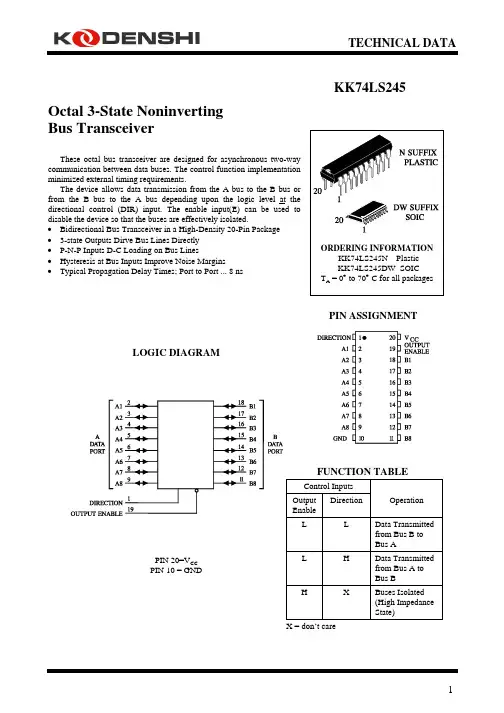
TECHNICAL DATAKK 74LS245Octal 3-State Noninverting Bus TransceiverThese octal bus transceiver are designed for asynchronous two-way communication between data buses. The control function implementation minimized external timing requirements.The device allows data transmission from the A bus to the B bus or from the B bus to the A bus depending upon the logic level at the directional control (DIR) input. The enable input(E) can be used to disable the device so that the buses are effectively isolated.• Bidirectional Bus Transceiver in a High-Density 20-Pin Package • 3-state Outputs Dirve Bus Lines Directly • P-N-P Inputs D-C Loading on Bus Lines• Hysteresis at Bus Inputs Improve Noise Margins• Typical Propagation Delay Times; Port to Port ... 8 nsPIN ASSIGNMENTLOGIC DIAGRAMPIN 20=V CC PIN 10 = GNDFUNCTION TABLEControl InputsOutput EnableDirection OperationL L Data Transmittedfrom Bus B to Bus A L H Data Transmittedfrom Bus A to Bus B H X Buses Isolated(High Impedance State) X = don’t careMAXIMUM RATINGS*Symbol Parameter ValueUnit V CC Supply Voltage 7.0 VV IN Input Voltage 7.0 VV OUT Output Voltage 5.5 VTstg Storage Temperature Range -65 to +150 °C*Maximum Ratings are those values beyond which damage to the device may occur.Functional operation should be restricted to the Recommended Operating Conditions.RECOMMENDED OPERATING CONDITIONSSymbol Parameter MinMaxUnit V CC Supply Voltage 4.75 5.25 VV IH High Level Input Voltage 2.0 VV IL Low Level Input Voltage 0.8 VI OH High Level Output Current -15 mAI OL Low Level Output Current 24 mAT A Ambient Temperature Range 0 +70 °CDC ELECTRICAL CHARACTERISTICS over full operating conditionsGuaranteedLimit Symbol Parameter TestConditions MinMaxUnit V IK Input Clamp Voltage V CC = min, I IN = -18 mA -1.5 VV OH High Level Output Voltage V CC = min, I OH = -1.0 mA 2.7 VV CC = min, I OH = -3.0 mA 2.4V CC = min, I OH = -15 mA 2.0V OL Low Level Output Voltage V CC = min, I OL = 12 mA 0.4 VV CC = min, I OL = 24 mA 0.5V T+ - V T-Hysteresis V CC = min 0.2 VI OZH Output Off Current HIGH V CC = max, V OUT = 2.7 V 20 µAI OZL Output Off Current LOW V CC = max, V OUT = 0.4 V -0.2 mAI IH High Level Input Current V CC = max, V IN = 2.7 V 20 µAV CC = max, V IN = 5.5 V (A or B) 0.1mAV CC = max, V IN = 7.0 Vfor Pin1, Pin 190.1I IL Low Level Input Current V CC = max, V IN = 0.4 V -0.2 mAI O Output Short Circuit Current V CC = max, V O =0 V(Note 1)-40 -225 mAI CC Supply OutputsHigh V CC = max 70 mA Current Outputs Low Outputs open 90All outputs disable 95Note 1: Not more thanone output should be shorted at a time, and duration of the short-circuit should not exceed one second.AC ELECTRICAL CHARACTERISTICS (T A = 25°C, V CC = 5.0 V, t r = 15 ns,,t f = 6.0 ns)Symbol Parameter TestConditionMinMaxUnitt PLH Propagation Delay Time, Low-to-High Level Output (from A or B to Output) 12nst PHL Propagation Delay Time, High-to-Low Level Output (from A or B to Output) C L = 45 pF,R L = 667 Ω12nst PZH Output Enable Time to High Level (from OE to Output) 40nst PZL Output Enable Time to Low Level (from OE to Output) 40nst PHZ Output Disable Time from High Level(from OE to Output) C L = 5 pF 25nst PLZ Output Disable Time from Low Level (from OE to Output) R L = 667 Ω 25nst PZL - S1 closed, S2 openedt PZH- S1 opened, S2 closedt PLZ, t PHZ - S1 and S2 closedFigure 1. Switching Waveforms(See Figure 3) Figure 2. Switching Waveforms(See Figure 4)NOTES A.C L includes probe and jig capacitance.B. All diodes are 1N916 or 1N3064.NOTES A.C L includes probe and jig capacitance.B. All diodes are 1N916 or 1N3064.Figure 3. Test Circuit Figure 4. Test CircuitEXPANDED LOGIC DIAGRAM。
74ls244中文资料
IOS
输出短路电流
VCC = Max (Note 3)
-40
-
-225
mA
ICC
电源电流
VCC = Max, Outputs Open
Outputs HIGH
-
13
23
mA
Outputs LOW
-
27
46
Outputs Disabled
-
32
54
74ls244中文资料
VO = 2.7V
-
-
20
μA
IOZL
输出高阻态时低电平电流
VO = 0.4V
-
-
-20
μA
II
最大输入电压时输入电流
VCC = Max
VI = 7V
-
-
0.1
mA
IIH
输入高电平电流
VCC = Max
VI = 2.7V
-
-
20
μA
IIL
输入低电平电流
VCC = Max
VI = 0.4V
-0.5
-
-200
输入钳位电压
VCC = Min, II = -18 mA
-
-
-1.5
V
HYS
Hysteresis (VT+ - VT-)
VCC = Min
0.2
0.4
-
V
VOH
输出高电平电压
VCC = Min, VIH = Min VIL = Max, IOH = -1 mA
2.7
-
-
V
VCC = Min, VIH = Min VIL = Max, IOH = -3 mA
HD74LS245P中文资料
Hitachi Code JEDEC EIAJWeight (reference value)DP-20N —Conforms 1.26 gUnit: mm元器件交易网Cautions1.Hitachi neither warrants nor grants licenses of any rights of Hitachi’s or any third party’s patent,copyright, trademark, or other intellectual property rights for information contained in this document.Hitachi bears no responsibility for problems that may arise with third party’s rights, includingintellectual property rights, in connection with use of the information contained in this document.2.Products and product specifications may be subject to change without notice. Confirm that you have received the latest product standards or specifications before final design, purchase or use.3.Hitachi makes every attempt to ensure that its products are of high quality and reliability. However,contact Hitachi’s sales office before using the product in an application that demands especially high quality and reliability or where its failure or malfunction may directly threaten human life or cause risk of bodily injury, such as aerospace, aeronautics, nuclear power, combustion control, transportation,traffic, safety equipment or medical equipment for life support.4.Design your application so that the product is used within the ranges guaranteed by Hitachi particularly for maximum rating, operating supply voltage range, heat radiation characteristics, installationconditions and other characteristics. Hitachi bears no responsibility for failure or damage when used beyond the guaranteed ranges. Even within the guaranteed ranges, consider normally foreseeable failure rates or failure modes in semiconductor devices and employ systemic measures such as fail-safes, so that the equipment incorporating Hitachi product does not cause bodily injury, fire or other consequential damage due to operation of the Hitachi product.5.This product is not designed to be radiation resistant.6.No one is permitted to reproduce or duplicate, in any form, the whole or part of this document without written approval from Hitachi.7.Contact Hitachi’s sales office for any questions regarding this document or Hitachi semiconductor products.Hitachi, Ltd.Semiconductor & Integrated Circuits.Nippon Bldg., 2-6-2, Ohte-machi, Chiyoda-ku, Tokyo 100-0004, Japan Tel: Tokyo (03) 3270-2111 Fax: (03) 3270-5109Copyright ' Hitachi, Ltd., 1999. All rights reserved. Printed in Japan.Hitachi Asia Pte. Ltd.16 Collyer Quay #20-00Hitachi TowerSingapore 049318Tel: 535-2100Fax: 535-1533URLNorthAmerica : http:/Europe : /hel/ecg Asia (Singapore): .sg/grp3/sicd/index.htm Asia (Taiwan): /E/Product/SICD_Frame.htm Asia (HongKong): /eng/bo/grp3/index.htm Japan : http://www.hitachi.co.jp/Sicd/indx.htmHitachi Asia Ltd.Taipei Branch Office3F, Hung Kuo Building. No.167, Tun-Hwa North Road, Taipei (105)Tel: <886> (2) 2718-3666Fax: <886> (2) 2718-8180Hitachi Asia (Hong Kong) Ltd.Group III (Electronic Components)7/F., North Tower, World Finance Centre,Harbour City, Canton Road, Tsim Sha Tsui,Kowloon, Hong Kong Tel: <852> (2) 735 9218Fax: <852> (2) 730 0281 Telex: 40815 HITEC HXHitachi Europe Ltd.Electronic Components Group.Whitebrook ParkLower Cookham Road MaidenheadBerkshire SL6 8YA, United Kingdom Tel: <44> (1628) 585000Fax: <44> (1628) 778322Hitachi Europe GmbHElectronic components Group Dornacher Stra§e 3D-85622 Feldkirchen, Munich GermanyTel: <49> (89) 9 9180-0Fax: <49> (89) 9 29 30 00Hitachi Semiconductor (America) Inc.179 East Tasman Drive,San Jose,CA 95134 Tel: <1> (408) 433-1990Fax: <1>(408) 433-0223For further information write to:。
74HC245中文资料_数据手册_参数
74HC245八路巴士TRANCEIVER;三态 14.修订历史表13:修订记录文档ID发布日期数据表状态更改注意文档.数取代版本 74HC_HCT245_3 20050131产品数据表 - 9397 750 14502 74HC_HCT245_CNV_2莫迪科幻阳离子: ? 本数据表的格式经过重新设计以符 合新的演示文稿和飞利浦半导体的信息标准 ?第4节“订购信息”,第6节“固定信息”和第13节“包装大纲“修改为包含DHVQFN20 包. 74HC_HCT245_CNV_2 19930930产品SPECI FI CATION 9397 750 14502 ? 74HC245 NV 2005.保留所有权利. 74HC245产品数据表 2005年1月3日至31日 13的22飞利浦半导体 74HC245; 74HCT245八 路巴士TRANCEIVER;三态 12.波形测量点在表11中给出. V OL 和V OH 是输出负载时发生的典型电压输出下降.图5.输入(AN,BN) 输出(BN,AN)传播延迟和输出转换时间测量点在表11中给出. V OL 和V OH 是输出负载时发生的典型电压输出下降.图6. 3态输出 启用和禁用时间表11:测量点类型输入产量 74HC245保留所有权利.产品数据表 2005年1月3日至3月31日 13的22飞利浦半导体 74HC245; 74HCT245八路公交车三态波形测量点在表 11中给出. V OL 和V OH 是输出负载时发生的典型电压输出降.图5.输入(An,Bn)输出(Bn,An)传播延迟和输出转换时间测量点 在表11中给出. V OL 和V OH 是输出负载时发生的典型电压输出降.图6. 3状态输出使能和禁止时间表11:测量点类型输入产量 V M V M 74HC245 0.5V CC 0.5V CC 74HCT245 1.3 V 1.3 V 001aac433 t PLH t PHL VM V M 90% 10% V M V M Bn,输出 An,Bn输入 V 我 GND V OH V OL t TLH t THL 001aac479 t PLZ t PHZ输出残输出启用 90% 10%输出启用 OE输入 V 我 V CC V OL V OH GND GND V M t PZL t PZH V M V M产量 LOW-到关关到LOW产量 74HC245输出频率; C L = pF中的输出负载电容; V CC =电源电压V; N =输入切换次数; Σ(C L ×V CC 2 ×f o )=输出和.表10:动态特 性类型74HCT245 GND = 0 V;测试电路见图7.符号参数条件敏典型马克斯单元 T amb = 25°C t PHL ,t PLH传播延迟A到Bn或Bn到安见 图5 V CC = 4.5 V - 12 22 NS V CC = 5.0 V; C L = 15pF - 10 - NS t PZH ,t PZL 3状态输出使能时间OE A或OE到Bn V CC = 4.5V; 见图6 1630ns PHZ ,t PLZ 3状态输出禁用时间OE A或OE到Bn V CC = 4.5V; 见图6 - 1630ns t THL ,t TLH输出转换时间 V CC = 4.5V; 见图5 - 五 12 NS C PD功耗电容每个收发器 V I = GND至V CC - 1.5 V [1] -30 - pF的 T amb = -40°C至+85°C t PHL ,t PLH传播延迟A到Bn或Bn到 安 V CC = 4.5V; 见图5 --28 NS t PZH ,t PZL 3状态输出使能时间OE A或OE到Bn V CC = 4.5V; 见图6 --38 NS PHZ ,t PLZ 3状态输出禁 用时间OE A或OE到Bn V CC = 4.5V; 见图6 --38 NS t THL ,t TLH输出转换时间 V CC = 4.5V; 见图5 --15 NS T amb = -40°C至+125°C t PHL ,t PLH传播延迟A到Bn或Bn到安 V CC = 4.5V; 见图5 --33 NS t PZH ,t PZL 3状态输出使能时间
74ls245原理
74ls245原理
74LS245是一种双向总线缓冲器,用于将一个电路中的双向数据总线
与另一个电路中的双向数据总线相连接。
它有两个8位数据输入/输出端口(Port A和Port B),并且可以通过一个控制管脚(有时称为“使能”管脚)来选择数据流的方向。
在74LS245中,控制管脚(通常称为“使能”管脚)是“OE”,意
为“输出使能”。
当OE管脚为高电平(通常为Vcc)时,数据可以从端口A到端口B传输,而当OE管脚为低电平(通常为地)时,数据
可以从端口B到端口A传输。
该芯片中还有三个重要的管脚:DIR,A和B。
DIR管脚的状态决定了数据流的方向,当DIR管脚为高电平时,数据从端口A到端口B传输,当DIR管脚为低电平时,数据从端口B到端口A传输。
在使用时,DIR管脚通常与控制器中的某个输出位相连,以实现数据的控制。
在使用74LS245时,需要注意以下几点:
1. 端口A和端口B的电压级别必须相同(通常为TTL电平或CMOS
电平)。
2. 当数据从一个电路传输到另一个电路时,要确保电路之间的电气特性匹配,以避免信号失真。
3. 在数据传输期间,DIR管脚和OE管脚必须设置为正确的状态以实现正确的数据流。
总之,74LS245是一个方便实用的双向总线缓冲器,可以确保数据流动的可靠性和正确性。
在实际应用中,75LS245可以用于传输数据,例如在电子设备和自动控制系统中用于数据输入和输出。
用74LS245读入数据实验
用74LS245读入数据实验一、实验目的1、了解89C51常用端口与总线连接的方法2、掌握用74LS245进行数据读入 二、实验说明当P0口总线负载达到或超出P0最大负载能力8个TTL 门时,必须接入总线驱动器。
74LS245即是双向数据总线驱动芯片,具有双向三态功能,既可以输出也可以输入数据,本实验中用作输入口。
74LS245的引脚如图所示:74LS245是8路同相三态双向总线收发器,可双向传输数据,传输方向由DIR 决定,当片选端E 低电平有效时,DIR=0,信号由B 向A 传输;DIR=1,由A 向B 传输;当E 为高电平时,A 、B 均成高阻态。
三、实验内容及步骤把读入值送入内存地址30H 中。
本实验用到单片机最小系统(F1区)、拨码开关(C7区)和74LS245模块(G1区)。
1、选取用89C51单片机最小应用系统模块,按照原理图连接电路,DIR 、G 端与地相连,74LS245的A0-7接单片机最小系统的PO 口JD4F ,74LS245的B0-7口接拨码开关(C7区)JD5B 。
打开相关的电源,短路帽插到VCC 处。
2、用串行数据通信线连接计算机与仿真器,把仿真器插到模块的锁紧插座中,请注意仿真器的方向:缺口朝上。
3、打开Keil uVision2仿真软件,首先建立本实验的项目文件,接着添加“TH25_74LS245.ASM ”源程序,进行编译,直到编译无误。
4、全速运行程序。
打开数据窗口(DATA),观察地址30H 的值,暂停程序。
再次观察30H 的值,是否已与拨码开关的值相同。
复位后,改变拨码开关输出,可再次运行程序,观察实验效果。
四、流程图及实验程序(见光盘中的程序文件夹)1、流程图 五、思考题试用74LS245输出数据。
六、电路图74LS245设置端口地址读入74LS245的值开始 结 束OE 19T/R 1A13B117A24B216A35B315A46B414A57B513A68B612A79B711A02B018VCC20GND10OE19T/R 1A13B117A24B216A35B315A46B414A57B513A68B612A79B711A02B018VCC20GND 10U1GSN74LS245N12345678JD2G B0-7VCCXTAL1A 12MHzC3A 33pFC2A 33pFP1.01P1.12P1.23P1.34P1.45P1.56P1.67P1.78RST 9P3.0/RXD 10P3.1/TXD 11P3.2/INT012P3.3/INT113P3.4/T014P3.5/T115P3.6/WR 16P3.7/RD 17XTAL218XTAL119VSS20P2.021P2.122P2.223P2.324P2.425P2.526P2.627P2.728PSEN 29ALE/PROG30EA31P0.032P0.133P0.234P0.335P0.436P0.537P0.638P0.739VCC 4089C51U1FVCC P3.0P3.1P1.0P1.1P1.2P1.3P1.4P1.5P1.6P1.7P0.0P0.1P0.2P0.3P0.4P0.5P0.6P0.7EAALE PSEN P2.7P2.6P2.5P2.4P2.3P2.2P2.1P2.0P3.2P3.3P3.4P3.5P3.6P3.7C3F 10uFVCCRESETR2F 100R1F 1K。
实验三 利用74LS245读入数据
实验三74LS245读入数据
一、实验目的
1、学习在单片机系统中扩展简单I/O 接口的方法。
2、了解CPU 常用的端口连接总线的方法。
3、掌握74LS245 进行数据读入或输出。
二、实验仪器与器件
Lab6000实验箱
三、实验原理
一般情况下,CPU 的总线会挂有很多器件,如何使这些器件不造成冲突,这就要使用一些总线隔离器件,例如74LS245 就是一种。
74LS245 是三态总线收发器,利用它既可以输出也可输入数据。
本实验74LS245 的片选地址为CSO,即8000H,读这个地址,就是从74LS245 读回开关的值。
可以用单步的方式执行程序,改变开关状态,观察读回的值。
四、实验内容及方法
1 硬件连线
1读入数据2 观察寄存器值
五、实验报告
1 写出利用74LS245原理
2 写出实验程序
3 至少3组读入寄存器数值
4 分析出现失败原因。
74LS244中文资料_数据手册_参数
Device Information(1)
PART NUMBER
PACKAGE
BODY SIZE (NOM)
SN54LS24x, SN54S24x
CDIP (20) – J CFP (20) – W LCCC (20) – FK
24.20 mm × 6.92 mm 7.02 mm × 13.72 mm 8.89 mm × 8.89 mm
Product Folder
Sample & Buy
Technical Documents
Tools & Software
Support & Community
SN54LS240, SN54LS241, SN54LS244, SN54S240, SN54S241, SN54S244 SN74LS240, SN74LS241, SN74LS244, SN74S240, SN74S241, SN74S244
8.2 Functional Block Diagrams ..................................... 11 8.3 Feature Description................................................. 12 8.4 Device Functional Modes........................................ 12 9 Application and Implementation ........................ 14 9.1 Application Information............................................ 14 9.2 Typical Application .................................................. 14 9.3 System Examples ................................................... 15 10 Power Supply Recommendations ..................... 17 11 Layout................................................................... 17 11.1 Layout Guidelines ................................................. 17 11.2 Layout Example .................................................... 17 12 Device and Documentation Support ................. 18 12.1 Related Links ........................................................ 18 12.2 Receiving Notification of Documentation Updates 18 12.3 Community Resource............................................ 18 12.4 Trademarks ........................................................... 18 12.5 Electrostatic Discharge Caution ............................ 18 12.6 Glossary ................................................................ 18 13 Mechanical, Packaging, and Orderable Information ........................................................... 19
单片机驱动芯片74HC245详细中文资料(16.5)
单片机驱动芯片(74HC245)详细中文资料(74HC245是一款高速CMOS器件,74HC245引脚兼容低功耗肖特基TTL(LSTTL)系列) 74HC245译码器可接受3位二进制加权地址输入(A0, A1和A2),并当使能时,提供8个互斥的低有效输出(Y0至Y7)。
74HC245特有3个使能输入端:两个低有效(E1和E2)和一个高有效(E3)。
除非E1和E2置低且E3置高,否则74HC138将保持所有输出为高。
利用这种复合使能特性,仅需4片7 4HC245芯片和1个反相器,即可轻松实现并行扩展,组合成为一个1-32(5线到32线)译码器。
任选一个低有效使能输入端作为数据输入,而把其余的使能输入端作为选通端,则74HC245亦可充当一个8输出多路分配器,未使用的使能输入端必须保持绑定在各自合适的高有效或低有效状态。
74HC245与74HC238逻辑功能一致,只不过74HC138为反相输出。
一、功能CD74HC245 ,CD74HC238和CD74HCT245, CD74HCT238是高速硅栅CMOS解码器,适合内存地址解码或数据路由应用。
74HC245作用原理于高性能的存贮译码或要求传输延迟时间短的数据传输系统,在高性能存贮器系统中,用这种译码器可以提高译码系统的效率。
将快速赋能电路用于高速存贮器时,译码器的延迟时间和存贮器的赋能时间通常小于存贮器的典型存取时间,这就是说由肖特基钳位的系统译码器所引起的有效系统延迟可以忽略不计。
HC138 按照三位二进制输入码和赋能输入条件,从8 个输出端中译出一个低电平输出。
两个低电平有效的赋能输入端和一个高电平有效的赋能输入端减少了扩展所需要的外接门或倒相器,扩展成24 线译码器不需外接门;扩展成32 线译码器,只需要接一个外接倒相器。
在解调器应用中,赋能输入端可用作数据输入端。
特性复合使能输入,轻松实现扩展兼容JEDEC标准no.7A 存储器芯片译码选择的理想选择低有效互斥输出 ESD保护 HBM EIA/JESD22-A114-C超过2000 V MM EIA/JESD22-A115-A超过200 V 温度范围 -4 0~+85 ℃ -40~+125 ℃多路分配功能74HC245是一款高速CMOS器件,74HC245引脚兼容低功耗肖特基TTL(LSTTL)系列。
- 1、下载文档前请自行甄别文档内容的完整性,平台不提供额外的编辑、内容补充、找答案等附加服务。
- 2、"仅部分预览"的文档,不可在线预览部分如存在完整性等问题,可反馈申请退款(可完整预览的文档不适用该条件!)。
- 3、如文档侵犯您的权益,请联系客服反馈,我们会尽快为您处理(人工客服工作时间:9:00-18:30)。
Device Information(1)
PART NUMBER
PACKAGE
BODY SIZE (NOM)
SN54LS245J
CDIP (20)
24.20 mm × 6.92 mm
SN54LS245W
CFP (20)
7.02 mm × 13.72 mm
SN54LS24 mm
Logic Diagram (Positive Logic)
1 DIR
19 OE
2 A1
18 B1
To Seven Other Channels
Copyright © 2016, Texas Instruments Incorporated
1
An IMPORTANT NOTICE at the end of this data sheet addresses availability, warranty, changes, use in safety-critical applications, intellectual property matters and other important disclaimers. PRODUCTION DATA.
8 ns
2 Applications
• Building Automation • Electronic Point of Sale • Factory Automation and Control • Test and Measurement
3 Description
These octal bus transceivers are designed for asynchronous two-way communication between data buses. The control-function implementation minimizes external timing requirements.
Product Folder
Sample & Buy
Technical Documents
Tools & Software
Support & Community
SN54LS245, SN74LS245
SDLS146B – OCTOBER 1976 – REVISED SEPTEMBER 2016
SNx4LS245 Octal Bus Transceivers With 3-State Outputs
The SNx4LS245 devices allow data transmission from the A bus to the B bus or from the B bus to the A bus, depending on the logic level at the directioncontrol (DIR) input. The output-enable (OE) input can disable the device so that the buses are effectively isolated.
1 Features
•1 3-State Outputs Drive Bus Lines Directly • PNP Inputs Reduce DC Loading on Bus Lines • Hysteresis at Bus Inputs Improves Noise Margins • Typical Propagation Delay Times Port to Port,
4 Revision History
NOTE: Page numbers for previous revisions may differ from page numbers in the current version.
Changes from Revision A (February 2002) to Revision B
Page
• Added ESD Ratings table, Feature Description section, Device Functional Modes, Application and Implementation section, Power Supply Recommendations section, Layout section, Device and Documentation Support section, and Mechanical, Packaging, and Orderable Information section .................................................................................................. 1
9.3 Feature Description................................................... 8 9.4 Device Functional Modes.......................................... 8 10 Application and Implementation........................ 10 10.1 Application Information.......................................... 10 10.2 Typical Application ............................................... 10 11 Power Supply Recommendations ..................... 12 12 Layout................................................................... 12 12.1 Layout Guidelines ................................................. 12 12.2 Layout Example .................................................... 12 13 Device and Documentation Support ................. 13 13.1 Related Links ........................................................ 13 13.2 Receiving Notification of Documentation Updates 13 13.3 Community Resource............................................ 13 13.4 Trademarks ........................................................... 13 13.5 Electrostatic Discharge Caution ............................ 13 13.6 Glossary ................................................................ 13 14 Mechanical, Packaging, and Orderable Information ........................................................... 13
SN74LS245DB
SSOP (20)
7.20 mm × 5.30 mm
SN74LS245DW
SOIC (20)
12.80 mm × 7.50 mm
SN74LS245N
PDIP (20)
24.33 mm × 6.35 mm