XP-143E XP243规格书
FPGA可编程逻辑器件芯片EP4SGX230FF35C2XN中文规格书
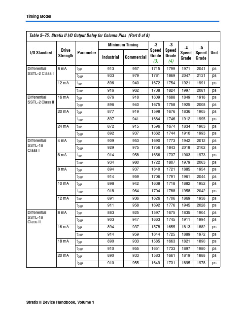
883
925
1597 1675 1835 1904 ps
903
947
1663 1745 1911 1994 ps
894
937
1578 1655 1813 1882 ps
914
959
1644 1725 1889 1972 ps
890
933
1585 1663 1821 1890 ps
910
955
1651 1733 1897 1980 ps
Stratix II Device Handbook, Volume 2
configuration file and cannot be dynamically controlled during user-mode operation.
(2) Only the CLKn pins on the top and bottom for the device feed to regional clock
896
940
1672 1754 1921 1991 ps
916
962
1738 1824 1997 2081 ps
876
918
1609 1688 1849 1918 ps
896
940
1675 1758 1925 2008 ps
877
919
1598 1676 1836 1905 ps
897
941
1664 1746 1912 1995 ps
Logic
Static Clock Select (1)
Enable/ Disable
Internal Logic
RCLK
Notes to Figure 1–53: (1) These clock select signals can only be dynamically controlled through a
设备比较表 新(1).ppt

4.BM123/BM221 PCB传输时间为4-5s,而SM321仅为2.5秒 5.BM喂料器精度不够,无取料补正功能造成0201元件精度速度大大降低,SM321有自动校正取料
YG300/L
1.YG300设备分区较多,传送时间太长,SM411采用平衡双轨传送PCB,传送时间为0秒 2. YG300是利用多模组提高速度,这样就限制了他的灵活性,转线时间慢 3.PCB范围小,YG300;330*250mm,YG300L;420*330mm; 4. YG300各头组分开工作,TABLE也移动,而三星的PCB平台是固定的 5.采用固定相机识别,元件需逐个扫描,识别时间长; 6.优化程序时,4个贴装头很难平衡(量大的物料必须多分几个料站才可以) 7.使用飞行吸嘴,搬入前允许高度4mm;使用标准吸嘴,搬入前允许高度6.5mm 8. YG300换料车互换性不强,YG300一次性换料车24个站位,其他YAMAHA设备是20个站位的 9. PCB传输时间为5s,而SM411采用双轨道,消除了传输时间 10.机械式喂料器,由三个支撑点固定,不耐用,抛料较高,SM411为滑槽式,经久耐用抛料少 11.贴装0201的物料抛料比较严重 12.需停机换料,影响实装效率 13.使用坦克链结构,容易磨损,且磨损后容易造成线路的托拽,从而导致难以预料的故障 14.能耗比SM411高出1倍还要多 15.采用不锈钢吸嘴,容易反白,易磁化。 16. YG300体积笨重4.5吨,每平方要求承受重量1600KG,只能在一楼才安全 17. YG300各头组分开工作,TABLE也移动,而三星的PCB平台是固定的
18.YG300PCB传送时间太长,如果有个头抛料后面都要等,也要浪费时间,一个区出现故障整台机器 都要停下,SM411采用平行双轨结构,双区互不影响,不会因为一个区的故障而影响整台机
XP243E的操作与调试

2.9电路板的取入和送出
自动运转中的 电路板可以自 动取入,也可 以在机器上输 入操作指令来 个别指示电路 板的取入/ 送出 动作。在换线 时如要检查搬 运轨道宽度、 传感器的动作 状态、或是送 出有缺陷的电 路板时,需要 用手动操作进 行电路板的取 入/ 送出。
操作步骤 1. 在[ 主画面] 上选择[ 机器操作]、[ 搬运轨道操作],显示出[ 搬运轨 道操作] 画面。 2. 要取入新的电路板时,按下[ 其他] 栏的[ 取入新电路板] 按键、要 排出电路板时,按 下[ 送出电路板] 按键,使其处于[ 启动] 按钮待机状态。 注意)XP-243 的时候,有必要输入电路板尺寸。此外,有缺口的电路 板请输入缺口尺寸。3. 按下[ 启动] 按钮后,进行取入/ 送出电路板。 电路板的取入/ 送出结束后,处于等待 下一步动作的状态。返回[ 主画面] 时,请按下[ 返回] 按键。
项目说明 料盘电梯的移动: 将料盘电梯移动到指定的料站上。在将指定料站以外的料盘盒供应给元件吸 取位臵时,从收存所供应的料盘盒移动到位臵上。当料盘吸取位臵上供应了料盘盒时,在 收存料盘盒后将料盘电梯移动到料盘更换位臵上。 往复臂前进: 往复臂前进指令是将按键按下的料站的料盘盒移动到元件的吸取位臵。 往复臂后退: 将在元件吸取位臵上所供应的料盘盒和料盘往复臂移动到料盘托架位臵。 料盘上面测量: 进行全部料站的上面测量。
2.12 元件自动吸取修正量
由于元件的位臵或者吸嘴的弯曲等各种各样的原因,在吸取元件时吸 嘴并不一定吸取元件中心。为了防止这种吸取元件的偏移,使用元件 的吸取位臵对X、Y 轴方向进行自动调整的功能。 元件数据的「Pick-up Auto Offset」项目设定为「0:YES」时,根据 影像处理的结果计算出吸取位臵的偏移量,自动补正在其元件以后吸 取的同类型的元件的位臵。 吸取补正值编辑 使用吸取补正值编辑器,可以参考、编辑吸取位臵补正量。 选择[ 生产]、[ 吸取补正值编辑],显示出[ 吸取补正值编辑] 画面。在 [ 吸取补正值编辑] 上可以参考、编辑吸取位臵补正量。 备注)在平台/ 料站号前显示出「*」记号的料站表示设定为料带宽度 8mm 的马达供料器。料带宽度设定为8mm 的马达供料器时,吸取 位臵向X 方向进行-2.0mm 修正。
XP143EXP243贴片机技术文件

XP143E/243E基础培训
Manual Operation截面中的 操作命令
XP143E/243E基础培训
Retract Head操作命令 的使用 点击Retract Head显示如下截面,机台左侧START按钮在
闪烁,按下start,则工作头会自动移到原点的位置
XP143E/243E基础培训
Conveyor Width操作命令 的使用 点击Conveyor Width显示以下截面,直接按左側向上或向下的箭头,可调节轨道的宽度,点击
Set to Program Value则可将程式中的轨道宽度值设定到机器中.还可以直接点击Program Value空白处显示数字键盘,直接输入PCB宽度值按下CR(确认)[ESC:取消,BS:清除],在保存到 程序值栏位中图2,然后点击Move按下START按钮,机器自行将轨道宽度调节到设定的參數 值(注:在调整轨道宽度时一定要确认轨道上无PCB和置件平台上无顶PIN后方可进行调整)
1
2
3
4
5
XP143E/243E基础培训
6
Select Program操作命 令的使用 Select program命令有两个来源,一个是主截面中production操作项,如
图1,另一个是主截面中program操作项, 如图2,点击所要的程式,再按下 download或download program,则程式被机器读取完成后点击close退出.
自动生产,pass代表机器作轨道用,idle1代表空打,但是会吸料,idle2也代表空打,但是机器 不会吸料;production mode有三个选择项:automatic代表自动置件,step代表半自动置件, 即动作一步就停下来,pause类似于step,不同的是动作几步停下来,按start又接着置 件;error handling有三个选择项:auto recovery代表自动补件,error stop代表出现错误就停 止,error pass代表出现错误忽略;recovery times代表自动补件的次数;scheduled panels代 表预设板子的数量;competed panels代表完成板子的数量;accel.rate代表机器的整体速度, 点击空白处可直接输入0.01到1之间增减速度,1代表100%
FPGA可编程逻辑器件芯片EP4SGX230KF40I3中文规格书
14.Hard Processor System I/O Pin MultiplexingThe Intel Agilex SoC has a total of 48 flexible I/O pins that are used for hard processor system (HPS) operation, external flash memories, and external peripheral communication. A pin multiplexing mechanism allows the SoC to use the flexible I/O pins in a wide range of configurations.Related InformationIntel Agilex Hard Processor System Technical Reference Manual Revision History on page 12For details on the document revision history of this chapter14.1. Features of the Intel Agilex HPS I/O BlockThe I/O block provides the following functionality and features:•Dedicated HPS I/O pins—48 pins available for HPS clock, external flash memories and peripherals.Note: The HPS also interfaces with an SDRAM memory controller . This interface is separate from the dedicated pins discussed in this chapter .•I/O multiplexing—Selects pins used by each HPS peripheral —Can expose HPS peripheral interfaces to FPGA logicNote: When routed to the FPGA, some HPS peripherals require additional pipeline support in the connected soft logic. Refer to the relevant HPS peripheral chapter for details.You configure I/O multiplexing when you instantiate the HPS component in Platform Designer.Related InformationExternal Memory Interface Handbook For details about memory I/O pins in the SoC hard memory controller , refer to the Functional Description - HPS Memory Controller chapter of the External Memory Interface Handbook .MNL-1100 | 2021.03.09Send FeedbackISO 9001:2015Registered14.2. Intel Agilex HPS I/O System IntegrationThe HPS I/O block consists of the following sub-blocks:•Dedicated pin multiplexers (MUXes) – MUXes for the dedicated I/O bank •FPGA access pin multiplexers – MUXes for HPS peripheral connections to the FPGA fabric •Register slave interface – Provides access to control registers, which allow the bootloader to initialize I/O pins and HPS peripheral interfaces at system startupRelated InformationIntel Agilex I/O Control Registers on page 18514.3. Functional Description of the HPS I/O14.3.1. I/O PinsThe HPS has 48 dedicated I/O pins. They are divided into four quadrants of 12 signals per quadrant. When you instantiate the HPS component in Platform Designer, you must assign one of the 48 pins as the HPS clock. You can then use the remaining dedicated I/O pins for other common peripherals.You can alternatively route most HPS peripherals (except USB) through the FPGA.Select this routing when you instantiate the HPS Component. For more information,refer to the Intel Agilex HPS Component Reference Manual .Note:When assigning an HPS peripheral to HPS dedicated pins, you must assign all peripheral I/O pins to the same quadrant, except for NANDx16, Trace, and GPIO.Note: Although the HPS dedicated I/O pins are configured through the control registers,software cannot reconfigure the pins after I/O configuration is complete. There is no support for dynamically changing the pin MUX selections for HPS dedicated I/O pins.Related Information•Booting and Configuration on page 512Details about the boot up process for the Intel Agilex HPS •FPGA Access on page 184Information about routing HPS peripheral interfaces to the FPGA •Configuring HPS I/O Multiplexing on page 188Information about configuring the HPS I/O MUXes14.3.2. FPGA AccessMost HPS peripheral interfaces can be connected into the FPGA fabric, instead of to the dedicated I/O pins.HPS peripherals connect to the FPGA fabric through the FPGA access pin MUX. When connected to the FPGA fabric, peripheral interfaces are exposed as ports of the HPS component.14.Hard Processor System I/O Pin MultiplexingMNL-1100 | 2021.03.09Send FeedbackNote: For warm resets, software can set the brgwarmmask registers to prevent theassertion of module reset signals to peripheral modules.When a module that has been held in reset is ready to start running, software can deassert the respective reset signal by writing to the following appropriate register .Modules Module Reset Signal RegisterFPGA fabrics2f_rst -s2f_cold_rst -s2f_watchdog_rst-Debug domain with CoreSight and Trace dbg_rst_ndbgmodrst.dbg_rst dbgmodrst.csdap_rst MPU corereset_n [3:0]mpumodrst.core[3:0]cpuporreset_n [3:0]coldmodrst.cpupor[3:0]l2reset_n coldmodrst.l2DMA dma_rst_n per0modrst.dmadma_ecc_rst_n per0modrst.dmaocpdma_periph_if_rst_n [7:0]per0modrst.dmaif[7:0]SPI Master and Slave spim_rst_n [1:0]per0modrst.spim[1:0]spis_rst_n [1:0]per0modrst.spis[1:0]Ethernet MAC emac_rst_n [2:0]per0modrst.emac[2:0]emac_ecc_rst_n [2:0]per0modrst.emac[2:0]ocpemac_ptp_rst_n per0modrst.emacptpUSB usb_rst_n [1:0]b[1:0]usb_ecc_rst_n [1:0]b[1:0]ocpNAND Flash nand_flash_rst_n per0modrst.nandnand_flash_ecc_rst_n per0modrst.nandocpSD/MMC sdmmc_rst_n per0modrst.sdmmcsdmmc_ecc_rst_n per0modrst.sdmmcocpWatchdog watchdog_rst_n [3:0]per1modrst.watchdog[3:0]Timer l4sys_timer_rst_n [1:0]per1modrst.l4systimer[1:0]sp_timer_rst_n [1:0]per1modrst.sptimer[1:0]I 2C i2c_rst_n [4:0]per1modrst.i2c[4:0]UART uart_rst_n [1:0]per1modrst.uart[1:0]GPIO gpio_rst_n [1:0]per1modrst.gpio[1:0]SoC-to-FPGA Bridge soc2fpga_bridge_rst_n brgmodrst.soc2fpgaFPGA-to-SoC Bridge fpga2soc_bridge_rst_n brgmodrst.fpga2socLightweight SoC-to-FPGA Bridge lwsoc2fpga_bridge_rst_n brgmodrst.lwsoc2fpgaMPFE mpfe_rst_nbrgmodrst.mpfe 13.Reset ManagerMNL-1100 | 2021.03.09Send Feedback。
XP243E_chinese_NEW

1.2 特 长
1.2.1 泛用性的扩大
1) 吸嘴收存数的扩大 为了对应丰富的异型元件,在吸嘴置放台上准备了可以增加到17个收存数 的类型。(选项) 因为收存数的增加,机械夹具或者特殊吸嘴也可以时常搭载。
9个吸嘴
17个吸嘴
2 )
対 象 部 品 の 拡 大
2) 对象元件的扩大 由于采用了高像素相机并研发了8mm料带宽的马达供料器,可以贴装0603的 极小的芯片元件。
-8-
CNT-XP243-03S
2.要 素
2.1 要 素
1500
2058 .5
1408 .5
2362
项目 电 源※1
气 源※2
机器尺寸 机器重量
要素
3相200V±10%(50/60Hz) 4kVA
0.5MPa
128L/min(A.N.R.) +170L/min(排出空料盘时:5sec) +55L/min(使用真空支撑销时) +2.8L/850ms(料带切刀时)
-2-
CNT-XP243-03S
1.概 要
1.2.2 本公司独特的“MSA”
贴装元件的识别全部由前光处理,使用本公司独特的“MSA”影像处理系 统。具有对应影像劣化和杂讯的能力。可以以高速进行识别处理。另外, 使用了对比度补正功能后,取入影像的对比度即使很小也可以稳定地进行 影像处理。更进一步,对于CSP等检查全部的bump。 MSA是被用称作为查找线的线所画的模板进行与元件的图形匹配。查找线是 在虚拟画面上以任意的位置、角度以及长度设定的线段并按其测定亮度。 对于对象物的轮廓垂直地画查找线后,可以求出轮廓线的位置。
2) 影像处理相机安装在滑轨一侧,贴装工作头从吸取元件到贴装点为止的移 动期间必须通过镜面上方,相机可以在一定的时间内得到静止影像。因此 贴装头可以用最短距离从吸取移动到实装位置,不会因贴装点的影像取入 的而发生移动损失。
FPGA可编程逻辑器件芯片EP4SGX230KF40C4中文规格书
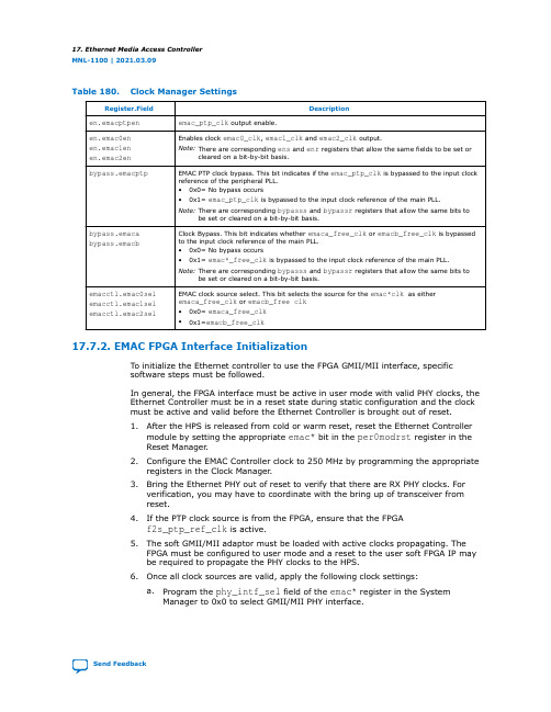
Table 180.Clock Manager Settings Register.FieldDescription en.emacptpenemac_ptp_clk output enable.en.emac0enen.emac1enen.emac2enEnables clock emac0_clk , emac1_clk and emac2_clk output.Note: There are corresponding ens and enr registers that allow the same fields to be set or cleared on a bit-by-bit basis.bypass.emacptp EMAC PTP clock bypass. This bit indicates if the emac_ptp_clk is bypassed to the input clockreference of the peripheral PLL.•0x0= No bypass occurs•0x1= emac_ptp_clk is bypassed to the input clock reference of the main PLL.Note: There are corresponding bypasss and bypassr registers that allow the same bits tobe set or cleared on a bit-by-bit basis.bypass.emacabypass.emacb Clock Bypass. This bit indicates whetheremaca_free_clk or emacb_free_clk is bypassed to the input clock reference of the main PLL.•0x0= No bypass occurs•0x1= emac*_free_clk is bypassed to the input clock reference of the main PLL.Note: There are corresponding bypasss and bypassr registers that allow the same bits tobe set or cleared on a bit-by-bit basis.emacctl.emac0selemacctl.emac1selemacctl.emac2sel EMAC clock source select. This bit selects the source for the emac*clk as either emaca_free_clk or emacb_free clk •0x0= emaca_free_clk •0x1=emacb_free_clk17.7.2. EMAC FPGA Interface InitializationTo initialize the Ethernet controller to use the FPGA GMII/MII interface, specific software steps must be followed.In general, the FPGA interface must be active in user mode with valid PHY clocks, the Ethernet Controller must be in a reset state during static configuration and the clock must be active and valid before the Ethernet Controller is brought out of reset.1.After the HPS is released from cold or warm reset, reset the Ethernet Controllermodule by setting the appropriate emac* bit in the per0modrst register in theReset Manager .2.Configure the EMAC Controller clock to 250 MHz by programming the appropriate registers in the Clock Manager .3.Bring the Ethernet PHY out of reset to verify that there are RX PHY clocks. For verification, you may have to coordinate with the bring up of transceiver from reset.4.If the PTP clock source is from the FPGA, ensure that the FPGAf2s_ptp_ref_clk is active.5.The soft GMII/MII adaptor must be loaded with active clocks propagating. The FPGA must be configured to user mode and a reset to the user soft FPGA IP may be required to propagate the PHY clocks to the HPS.6.Once all clock sources are valid, apply the following clock settings:a.Program the phy_intf_sel field of the emac* register in the SystemManager to 0x0 to select GMII/MII PHY interface.17.Ethernet Media Access ControllerMNL-1100 | 2021.03.09Send Feedbackb.If the PTP clock source is from the FPGA, set the ptp_clk_sel bit to 0x1 in the emac_global register of the System Manager .c.Enable the Ethernet Controller FPGA interface by setting the emac_* bit in the fpgaintf_en_3 register of the System Manager .7.Configure all of the EMAC static settings if the user requires a different setting from the default value. These settings include the AxPROT[1:0] and AxCACHEsignal values which are programmed in the emac* register of the System Manager .8.After confirming the settings are valid, software can clear the emac* bit in theper0modrst register of the Reset Manager to bring the EMAC out of reset..When these steps are completed, general Ethernet controller and DMA software initialization and configuration can continue.Note: These same steps can be applied to convert the HPS GMII to an RGMII, RMII or SGMII interface through the FPGA, except that in step 5 during FPGA configuration, you would load the appropriate soft adaptor for the interface and apply reset to it as well.The PHY interface select encoding would remain as 0x0. For the SGMII interface additional external transceiver logic would be required. Routing the Ethernet signals through the FPGA is useful for designs that are pin-limited in the HPS.17.7.3. EMAC HPS Interface InitializationTo initialize the Ethernet controller to use the HPS interface, specific software steps must be followed including selecting the correct PHY interface through the System Manager .In general, the Ethernet Controller must be in a reset state during static configuration and the clock must be active and valid before the Ethernet Controller is brought out of reset.1.After the HPS is released from cold or warm reset, reset the Ethernet Controllermodule by setting the appropriate emac* bit in the per0modrst register in theReset Manager .2.Configure the EMAC Controller clock to 250 MHz by programming the appropriate registers in the Clock Manager .3.Bring the Ethernet PHY out of reset to allow PHY to generate RX clocks.There are no registers to verify, but you can create the following custom logic block to cross check:•If the RX clock is routed through FPGA IO—you can use Signal Tap to check, or create a simple counter block with the RX clock as clock source to check if it runs.•If the RX clock is routed as HPS IO—you need to explore if the kernel application code is able to source through RX clock to check its status.4.When all the clocks are valid, program the following clock settings:a.Program the phy_intf_sel field of the emac* register in the SystemManager to 0x1 or 0x2 to select RGMII or RMII PHY interface.b.Disable the Ethernet Controller FPGA interface by clearing the emac_* bit inthe fpgaintf_en_3 register of the System Manager .17.Ethernet Media Access ControllerMNL-1100 | 2021.03.09Send Feedback5.Configure all of the EMAC static settings if the user requires a different setting from the default value. These settings include the AxPROT[1:0] and AxCACHEsignal values, which are programmed in the emac* register of the SystemManager .6.Execute a register read back to confirm the clock and static configuration settings are valid.7.After confirming the settings are valid, software can clear the emac* bit in theper0modrst register of the Reset Manager to bring the EMAC out of reset.When these steps are completed, general Ethernet controller and DMA software initialization and configuration can continue.17.7.4. DMA InitializationThis section provides the instructions for initializing the DMA registers in the proper sequence. This initialization sequence can be done after the EMAC interface initialization has been completed. Perform the following steps to initialize the DMA:1.Provide a software reset to reset all of the EMAC internal registers and logic. (DMA Register 0 (Bus Mode Register) – bit 0). †2.Wait for the completion of the reset process (poll bit 0 of the DMA Register 0 (Bus Mode Register), which is only cleared after the reset operation is completed). †3.Poll the bits of Register 11 (AXI Status) to confirm that all previously initiated (before software reset) or ongoing transactions are complete.Note: If the application cannot poll the register after soft reset (because of performance reasons), then it is recommended that you continue with the next steps and check this register again (as mentioned in step 12 on page 382)before triggering the DMA operations.†4.Program the following fields to initialize the Bus Mode Register by setting values in DMA Register 0 (Bus Mode Register):†•Mixed Burst and AAL •Fixed burst or undefined burst †•Burst length values and burst mode values †•Descriptor Length (only valid if Ring Mode is used)†5.Program the interface options in Register 10 (AXI Bus Mode Register). If fixed burst-length is enabled, then select the maximum burst-length possible on the bus (bits[7:1]).†6.Create a proper descriptor chain for transmit and receive. In addition, ensure that the receive descriptors are owned by DMA (bit 31 of descriptor should be set).When OSF mode is used, at least two descriptors are required.7.Make sure that your software creates three or more different transmit or receive descriptors in the chain before reusing any of the descriptors.†8.Initialize receive and transmit descriptor list address with the base address of the transmit and receive descriptor (Register 3 (Receive Descriptor List Address Register) and Register 4 (Transmit Descriptor List Address Register) respectively).†9.Program the following fields to initialize the mode of operation in Register 6(Operation Mode Register):17.Ethernet Media Access ControllerMNL-1100 | 2021.03.09Send Feedback。
XP243E的操作与调试解析

2.5 蜂鸣器的停止
• 蜂鸣器鸣响时的停 止方法。 方法一:触摸画面 左上方的[FUJI] 标 记,显示出以下的 画面后,按下[ 蜂 鸣器关] 的按钮。 方法二:按下[ 周 期停止] 的按钮后, 停止蜂鸣器。
2.7贴装头待机
• 操作等待时候, 可将贴装头移动 到退让位置。 操作步骤 • 1. 在[ 主画面] 上 选择[ 机器操作]、 [ 贴装头待机]。 • 2. 按下[ 启动] 键, 把贴装头移动到 退让位置。
控制电源 开关
按下此按钮后机器接通控制电源,启动机器的控制软件。
可以设定选择使用SIDE 1 或SIDE 2 中的某一侧( 相反侧) 来进 SIDE 1/2 行机器操作。将此开关设定在「LOCK」位置时,相反的SIDE 侧 ENABLE/ 解除[ 紧急停止] 按钮,另外,在此时只要不将「LOCK」2. 位置 上设定的SIDE 侧的开关变为「ENABLE」,则从相反侧的SIDE 不 LOCK 能解除机器操作的锁定。
主菜单
• F: 选择在各画面上主区域内的操作指令键后,可以进入到下一层的相关操作 指令中去。
2.基本操作
2.1 机器的启动和关机
操作步骤 • 1. 启动与机器相连接的监控电 脑。 • 2. 把机器上的电源总开关置于 “ON”的位置。 • 3. 按下[ 接通控制电源] 按钮 后启动机器。机器启动后,此 时显示[Logon] 画面。 • 4. 选择[Operator] ( 操作者名) 或者[Password] ( 密码) 的输入 框后显示出键盘。 • 5. 用画面上显示的键盘上输入 [Operator]( 操作者名) 和 [Password]( 密码),选择 [Logon]键进行注册。
蜂鸣器
机器出现异常时发出报警声。 按下此按钮会切断动力电源并立即停止机器的运行。因为此按