爱普生晶振SG-8002LB可编程晶体振荡器规格书
爱普生osc有源晶振 SG-9101CB晶体振荡器 规格书资料

►Designed for automotive applications such as Car Multimedia, Body Electronics, Remote Keyless Entry etc.
►Designed for automotive applications related to driving safety (Engine Control Unit, Air Bag, ESC etc ).
NOTICE:PLEASE READ CAREFULLY BELOW BEFORE THE USE OF THIS DOCUMENT ©Seiko Epson Corporation 2020 ――――――――――――――――――――――――――――――――――――――――――――――――――――
1. The content of this document is subject to change without notice. Before purchasing or using Epson products, please contact with sales representative of Seiko Epson Corporation (“Epson”) for the latest information and be always sure to check the latest information published on Epson’s official web sites and resources.
All of our major manufacturing and non-manufacturing sites, in Japan and overseas, completed the acquisition of ISO 14001
Micrel DSC8002 1.8V至3.3V可编程低功耗CMOS振荡器说明书
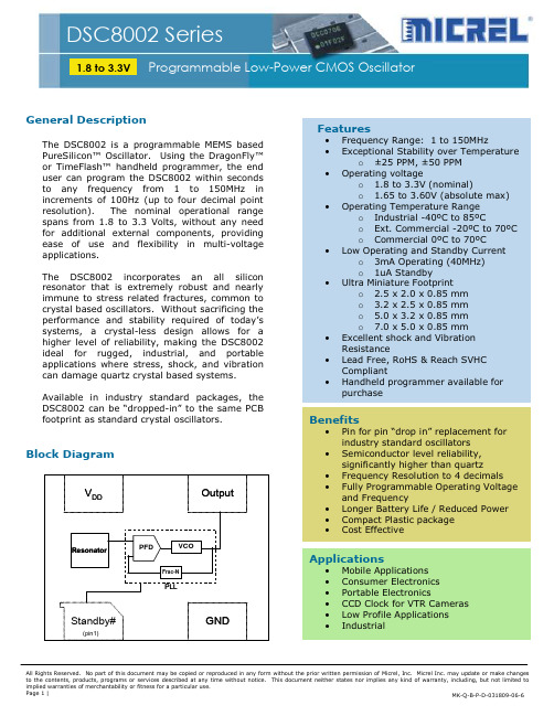
1.8 to 3.3VGeneral DescriptionThe DSC8002 is a programmable MEMS based PureSilicon™ O scillator. Using the DragonFly™ or TimeFlash™ handheld programmer, the end user can program the DSC8002 within seconds to any frequency from 1 to 150MHz in increments of 100Hz (up to four decimal point resolution). The nominal operational range spans from 1.8 to 3.3 Volts, without any need for additional external components, providing ease of use and flexibility in multi-voltage applications.The DSC8002 incorporates an all silicon resonator that is extremely robust and nearly immune to stress related fractures, common to crystal based oscillators. Without sacrificing the performance and stability required of today’s systems, a crystal-less design allows for a higher level of reliability, making the DSC8002 ideal for rugged, industrial, and portable applications where stress, shock, and vibration can damage quartz crystal based systems.Available in industry standard packages, the DSC8002 can be “dropped-in” to the same PCB footprint as standard crystal oscillators. Block DiagramFeatures∙Frequency Range: 1 to 150MHz∙Exceptional Stability over Temperature o±25 PPM, ±50 PPM∙Operating voltageo 1.8 to 3.3V (nominal)o 1.65 to 3.60V (absolute max) ∙Operating Temperature Rangeo Industrial -40ºC to 85ºCo Ext. Commercial -20ºC to 70ºCo Commercial 0ºC to 70ºC ∙Low Operating and Standby Currento3mA Operating (40MHz)o1uA Standby∙Ultra Miniature Footprinto 2.5 x 2.0 x 0.85 mmo 3.2 x 2.5 x 0.85 mmo 5.0 x 3.2 x 0.85 mmo7.0 x 5.0 x 0.85 mm∙Excellent shock and VibrationResistance∙Lead Free, RoHS & Reach SVHCCompliant∙Handheld programmer available for purchaseBenefits∙Pin for pin “d rop in” replacement for industry standard oscillators∙Semiconductor level reliability,significantly higher than quartz ∙Frequency Resolution to 4 decimals∙Fully Programmable Operating Voltage and Frequency∙Longer Battery Life / Reduced Power∙Compact Plastic package∙Cost EffectiveApplications∙Mobile Applications∙Consumer Electronics∙Portable Electronics∙CCD Clock for VTR Cameras∙Low Profile Applications∙Industrial1.8 to 3.3V1Ordering CodeSpecifications1. Absolute maximum ratings are those values beyond which the safety of the device cannot be guaranteed. The device should not beoperated beyond these limits.2. Output frequency to within 100ppm of final stable output frequency.3. See typical cycle to cycle jitter graph for frequency dependence.* See Ordering Information for detailsNominal Performance Characteristics 1.8V Characteristics3.3V CharacteristicsOutput WaveformStandby FunctionTest CircuitV DD15pF*V SD 50% OutputStandby#Board Layout (recommended)Solder Reflow ProfilePackage DimensionsT e m p e r a t u r e (°C )200°217°150°25°260°3.2 x 2.5 mm Plastic Package2.5 x 2.0 mm Plastic PackageOrdering InformationDSC8002 PTS – TDisclaimer:Micrel makes no representations or warranties with respect to the accuracy or completeness of the information furnished in this data sheet. This information is not intended as a warranty and Micrel does not assume responsibility for its use. Micrel reserves the right to change circuitry, specifications and descriptions at any time without notice. No license, whether express, implied, arising by estoppel or otherwise, to any intellectual property rights is granted by this document. Except as provided in Micrel’s terms and conditions of sale for such products, Micrel assumes no liability whatsoever, and Micrel disclaims any express or implied warranty relating to the sale and/or use of Micrel products including liability or warranties relating to fitness for a particular purpose, merchantability, or infringement of any patent, copyright or other intellectual property right. MICREL, Inc. ● 2180 Fortune Drive, San Jose, California 95131 ● USAPhone: +1 (408) 944-0800 ● Fax: +1 (408) 474-1000 ● Email:******************● 。
epson晶振选型手册
Epson晶振选型手册引言概述:Epson晶振选型手册是一本提供关于Epson晶振选型的专业指导手册。
晶振作为一种重要的电子钟振装置,广泛应用于各类电子设备中,对于设备的稳定性和精准性起到关键作用。
本手册将从多个方面介绍Epson晶振的选型原则和方法,以帮助读者准确选型和应用。
正文内容:1. 晶振的基本原理1.1 晶振的作用与功能1.1.1 提供时钟信号1.1.2 稳定电子设备的工作频率1.1.3 控制和同步各设备之间的通信1.1.4 精确计时和定时功能1.2 晶振的工作原理1.2.1 晶体振荡原理1.2.2 纯谐振条件与频率稳定性1.2.3 晶振的构造与材料选择2. Epson晶振的特点与优势2.1 高稳定性和低功耗2.1.1 稳定性与频率偏移2.1.2 低功耗对电池寿命的影响2.2 宽温度范围和长寿命2.2.1 温度对晶振频率的影响2.2.2 长期使用的可靠性和稳定性2.3 大容量和小封装尺寸2.3.1 容量对数据传输速率的影响2.3.2 封装尺寸对电路板设计的要求3. Epson晶振选型原则3.1 需求分析和参数确定3.1.1 设备类型和用途3.1.2 工作频率和精度要求3.1.3 温度范围和环境影响3.2 选择适合的晶振类型3.2.1 晶振频率范围和精度等级3.2.2 温度补偿和温度响应特性3.2.3 封装尺寸和安装要求3.3 参考设计和测试验证3.3.1 参考电路设计3.3.2 振荡电路测试和频率测量3.3.3 选型结果评估和优化4. Epson晶振选型案例分析4.1 移动方式晶振选型4.1.1 高稳定性和小封装尺寸的需求4.1.2 多频段应用的选择考虑4.2 电子表计晶振选型4.2.1 长期使用和温度范围要求4.2.2 低功耗和电池寿命的平衡4.3 工业自动化控制晶振选型4.3.1 高频率和精度要求4.3.2 多通道同步和控制4.3.3 长寿命和可靠性的考虑5. Epson晶振应用注意事项5.1 环境温度和封装要求5.2 抗振动和抗干扰性能5.3 防静电措施和电源干扰5.4 长期使用和老化问题结语:本手册全面介绍了Epson晶振的选型原则和方法,包括晶振的基本原理、Epson晶振的特点与优势、选型原则、案例分析以及应用注意事项。
爱普生(EPSON)高精度晶体振荡器TG-5006CJ CE CG规格书
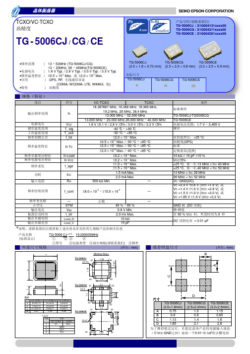
±0.2 × 10⁻⁶ Max. ±0.2 × 10⁻⁶ Max. ±1.0 × 10⁻⁶ Max. ±1.5 × 10⁻⁶ Max.
+25 °C (GPS)
()
10 kΩ // 10 pF ±10 %
VCC±5%
+25 °C,
,13 MHz ≤ f0≤ 40 MHz
●为汽车行驶安全方面的应用(引擎控制单元、气囊、电子稳定程序控制系统)。
注意事项
·本材料如有变更,恕不另行通知。量产设计时请确认最新信息。 ·未经 Seiko Epson 公司书面授权,禁止以任何形式或任何方式复制或者发布本材料中任何部分的信息内容。 ·本材料中的书面信息、应用电路、编程、使用等内容仅供参考。Seiko Epson 公司对第三方专利或版权的侵权行为不负有任何责任。本材料
A
0.75
1.0
1.15
B
0.6
0.8
0.85
C
1.13
1.4
1.6
D
1.65
2.1
2.6
VCC-GND
0.01~0.1uF
推进环境管理体系 符合国际标准
在环境管理体系的运行方面,使用 ISO14001 国际环境标准,通过“计 划-实施-检查-验证(PDCA)的循环来实现持续改进。公司位于日本和 海外的主要制造基地已取得了 ISO14001 资格认证。
b
(d )
#4
TG-5006CG #1 C0.2
1.2
#3
2.1
#2
c
1.5
TG-5006CJ TG-5006CG TG-5006CE
8002D使用说明书
的屏上,水平
修正9步
4:3的输入信
号显示在16:9 L H H L 的屏上,水平
修 正 15 步 并 翻
转Wide 2序列
在 Wide 1 left
显示模式下将
L H L H 4:3的输入信 号显示在16:9 的屏上
在 Normal left 显示模式下将
L
H
L
L 4:3的输入信
号显示在16:9
的屏上
二.特征
z 支持 16 种 16:9 的显示模式 z 支持 16 种水平显示解析模式,解析分辨率 240~2880 z 最大主时钟频率是 28.9MHz,提供 2 分频模式 z 支持内、外部主时钟输入 z 支持内、外部垂直同步信号输入 z 自动检测 NTSC 和 PAL 制式 z 自动检测同步输入信号的极性 z VCO 和 H-POS 独立调整 z 支持条带和增量两种颜色排列模式 z V-POS 最大 15 行的调整范围 z 支持源和栅驱动控制时序 z 源驱动控制提供 3 相时钟 z 支持外部 RGB 控制解码和放大信号 z 支持翻转和镜像扫描控制 z 行逆向驱动方案 z 电源电压 5V/3.3V z LQFP64 封装
1
三、管脚图
2
四.引脚说明:
序号 1 2
名称 VCC CSY
I/O
描
述
电源
I 复合同步或外部时钟输入
备注 注释 1
3 RS4
4 RS3 5 RS2
I 解析模式设置端
注释 2
6 RS1
7 DM4
8 DM3 9 DM2
I 显示模式设置端
缺省为高
10 DM1 11 SDC 12 DLT 13 HPO 14 HPI
O 输出 VCOM 信号极性 O 视频极性选择信号
晶体振荡器产品说明书
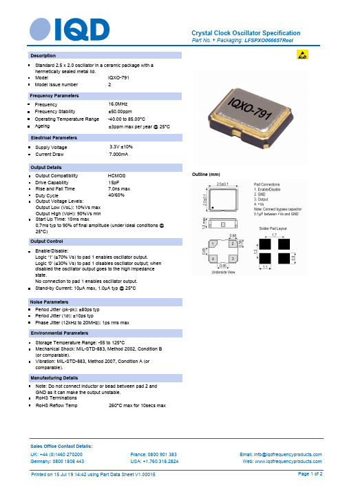
Outline (mm)DescriptionStandard 2.5 x 2.0 oscillator in a ceramic package with a hermetically sealed metal lid.IQXO-791Model Model Issue number 2Frequency ParametersFrequency16.0MHz Frequency Stability±50.00ppm -40.00 to 85.00°C Operating Temperature RangeAgeing±3ppm max per year @ 25°CElectrical Parameters 3.3V ±10%Supply Voltage7.000mACurrent DrawOutput Details Output CompatibilityHCMOS Drive Capability 15pF7.0ns maxRise and Fall Time 40/60%Duty CycleOutput Voltage Levels:Output Low (VoL): 10%Vs maxOutput High (VoH): 90%Vs minStart Up Time: 10ms max0.7ms typ to 90% of final amplitude (under ideal conditions @ 25°C)Output Control Enable/Disable:Logic ‘1’ (≥70% Vs) to pad 1 enables oscillator output.Logic ‘0’ (≤30% Vs) to pad 1 disables oscillator output; when disabled the oscillator output goes to the high impedance state.No connection to pad 1 enables oscillator output.Stand-by Current: 10μA max, 1.0µA typ @ 25°CNoise ParametersPeriod Jitter (pk-pk): ±80ps typPeriod Jitter (1σ): ±10ps typPhase Jitter (12kHz to 20MHz): 1ps rms maxEnvironmental ParametersStorage Temperature Range: -55 to 125°CMechanical Shock: MIL-STD-883, Method 2002, Condition B (or comparable).Vibration: MIL-STD-883, Method 2007, Condition A (or comparable).Manufacturing DetailsNote: Do not connect inductor or bead between pad 2 and GND as it can make the output unstable.RoHS TerminationsRoHS Reflow Temp 260°C max for 10secs max Sales Office Contact Details:USA: +1.760.318.2824France: 0800 901 383UK: +44 (0)1460 270200Web: ComplianceCompliant RoHS Status (2011/65/EU)Compliant REACh StatusMSL Rating (JDEC-STD-033):Not ApplicablePackaging Details Tape & reel in accordance with EIA-481DPack Style: ReelPack Size: 3,000Alternative packing option available Sales Office Contact Details:USA: +1.760.318.2824France: 0800 901 383UK: +44 (0)1460 270200Germany************Email:*****************************Web: 。
贴片晶振规格书_范文模板及概述
贴片晶振规格书范文模板及概述1. 引言1.1 概述贴片晶振是一种常见的电子元件,被广泛应用于各种电子设备中。
它具有稳定的频率输出和精确的时间基准,能够提供准确可靠的时钟信号给其他组件或系统使用。
贴片晶振规格书作为对该元件性能和参数的详细说明和要求,对于设计、生产和应用方面都具有重要意义。
1.2 文章结构本文将首先简要介绍贴片晶振规格书的概述,包括其定义、作用以及发展历程和应用领域等内容。
接着,我们将提供一个贴片晶振规格书模板,包含基本信息部分、电气特性部分和动态参数部分等内容,并解释每个部分所需信息的含义和作用。
此外,我们还将讨论贴片晶振规格书编写的重点,包括规范格式和语言表达要求、关键参数与测试方法说明以及典型应用场景案例分析等方面。
最后,我们将总结本文内容并探讨贴片晶振规格书发展趋势。
1.3 目的本文旨在提供一篇关于贴片晶振规格书的范文模板以及详细概述,帮助读者了解贴片晶振规格书的基本结构和编写要点。
通过阅读本文,读者将能够更好地理解贴片晶振规格书的重要性和应用,掌握撰写贴片晶振规格书的方法和技巧,并对贴片晶振规格书未来发展趋势有所展望。
2. 贴片晶振规格书概述2.1 贴片晶振的定义和作用:贴片晶振是一种小型化的电子元件,广泛应用于各种电路中以提供稳定的时钟信号。
它由一个晶体谐振器、固定电容和金属外壳组成。
晶体谐振器通过外部激励产生震荡信号,并将其转换为频率固定的时钟信号。
贴片晶振是整个电子系统中重要的时基来源,对于保证精确的计时和数据传输至关重要。
2.2 发展历程和应用领域:贴片晶振自问世以来,在电子行业中取得了长足的发展。
随着电子产品需求越来越小型化、高性能化和高可靠性等要求,贴片晶振逐渐取代了传统封装形式的振荡器,成为主流选择。
贴片晶振广泛应用于许多领域,包括通信设备、计算机硬件、消费类电子产品和工业控制等。
在通信设备中,贴片晶振被用于网络路由器、交换机以及无线通信设备等;在计算机硬件中,贴片晶振广泛应用于主板、显卡和存储设备等;在消费类电子产品中,如智能手机、平板电脑和手持设备等,也都需要贴片晶振作为时钟源。
爱普生晶振SG-8002CE可编程晶体振荡器规格书
30 mA Max.
-
25 mA Max.
16 mA Max. 16 mA Max.
OE=GND (PT.PH,PC) ( SG-8002LB) OE=GND (PH,PC) ( SG-8002LB)
I_std
50 µA Max.
ST =GND (ST,SH,SC)
40 % ~ 60 %
-
TTL load: 1.4 V ,
CMOS *1 L_CMOS
-
15 pF Max.
(SG-8002LB)
15 pF Max.
25 pF Max
15 pF Max. (SG-8002CA / JA / DC / DB)
VIH VIL
2.0 V Min. 0.8 V Max.
70 % VCC Min. 20 % VCC Max.
OE
ST
1.4 -0.15
5.08
1.6
2.54
1.8 C (ex. 0.01 µF)
Resist 5.08
SG-8002JC
10. 5 Max.
#4
#3
SOJ 4pin 10.5x5.8x2.7 mm
Package and pin compatible with SG-636.
1.3
5. 0 5.8 Max.
#1 13.7 Max. #4
7. 62
SG-8002DB
DIP full size
#14
#8
6. 36
16.0000 C 2PH EPSON 9357B
#1 19.8 Max. #7 7.62
0.51
0.2M in .
7. 62
90 °~ 105 °
爱普生(EPSON)高精度晶体振荡器TG-5035CJ CG CE规格书
-40 °C ~ +90 °C
-40 °C ~ +85 °C / -30 °C ~ +85 °C ±2.0 × 10⁻⁶ Max.
±0.5 × 10⁻⁶ Max. / -30 °C ~ +85 °C ±2.0 × 10⁻⁶ Max. / -30 °C ~ +85 °C ±0.5 × 10⁻⁶ Max. / -40 °C ~ +85 °C
+25 °C,
,40 MHz < f0≤ 52 MHz
10 MHz ≤ f0≤ 26 MHz
26 MHz < f0≤ 52 MHz
ST =GND
ST
Vc-GND(DC)
VC =0.9 V ±0.6 V (VCC =1.8 V) VC =1.4 V ±1.0 V (VCC =2.8 V) VC =1.5 V ±1.0 V (VCC =3.0 V) VC =1.65 V ±1.0 V (VCC =3.3 V)
ISO/TS16949 是一项国际标准,是在 ISO9001 的基础上增 加了对汽车工业的特殊要求部分。
关于在目录内使用的记号
●无铅。
●符合欧盟 RoHS 指令。 欧盟 RoHS 指令免检的含铅产品。 (密封玻璃、高温熔化性焊料或其他材料中包含铅。)
●为汽车方面的应用,如汽车多媒体、车身电子、遥控无钥门锁等。
TG-5035CJ
TG-5035CG
TG-5035CE
•
: 1.8 V Typ./ 2.8 V Typ./ 3.0 V Typ./ 3.3 V Typ.
(2.0 × 1.6 × 0.73 mm) (2.5 × 2.0 × 0.8 mm) (3.2 × 2.5 × 0.9 mm)
爱普生晶振最小包装数量_标准包装规格
L L L L L L L L L L L L L L L L L L L L L L L L L L L
【南京南山:EPSON晶振代理证书编号14013】
●SAW 谐振器
型号 FS-335 FS-555 FS-585 NS-21R NS-32R 数量 (件/卷筒) 4000 4000 4000 3000 4000 1000 3000 3000 3000 1000 1000 2000 1000 2000 2000 2000 1000 1000 1000 1000 1000 1000 1000 1000 1000 1000 1000 1000 1000 1000 1000 1000 1000 1000 2000 1000 1000 1000 2000 1000 2000 3000 1000 2000 1000 1000 2000 1000 1000 1000 1000 2000 1000 1000 1000 1000 12000 2000 2000 12000 1000 1000 1000 1000 a Φ330 Φ330 Φ330 Φ180 Φ330 Φ254 Φ180 Φ180 Φ180 Φ330 Φ254 Φ180 Φ330 Φ180 Φ180 Φ180 Φ180 Φ330 Φ330 Φ254 Φ254 Φ180 Φ254 Φ180 Φ180 Φ180 Φ180 Φ180 Φ180 Φ180 Φ180 Φ180 Φ180 Φ254 Φ180 Φ330 Φ330 Φ254 Φ254 Φ254 Φ180 Φ180 Φ254 Φ254 Φ254 Φ330 Φ254 Φ330 Φ330 Φ254 Φ180 Φ180 Φ254 Φ180 Φ180 Φ180 Φ330 Φ180 Φ180 Φ330 Φ180 Φ180 Φ254 Φ180 卷筒尺寸 b Φ80 or Φ100 Φ80 or Φ100 Φ80 or Φ100 Φ60 Φ80 or Φ100 Φ100 Φ60 Φ60 Φ60 Φ80 or Φ100 Φ100 Φ60 Φ80 or Φ100 Φ60 Φ60 Φ60 Φ60 Φ80 or Φ100 Φ80 or Φ100 Φ100 Φ100 Φ60 Φ100 Φ60 Φ60 Φ60 Φ60 Φ60 Φ60 Φ60 Φ60 Φ60 Φ60 Φ100 Φ60 Φ80 or Φ100 Φ80 or Φ100 Φ100 Φ100 Φ100 Φ60 Φ60 Φ100 Φ100 Φ100 Φ80 or Φ100 Φ100 Φ80 Φ80 Φ100 Φ60 Φ60 Φ100 Φ60 Φ60 Φ60 Φ100 Φ60 Φ60 Φ100 Φ60 Φ60 Φ100 Φ60 W 13.5 13.5 13.5 9.0 13.5 17.5 9 9 13 17.5 17.5 13 17.5 13 9 9 13 25.5 17.5 17.5 17.5 17 17.5 13 13 13 17 17 17 17 13 17 13 17.5 9 25.5 17.5 17.5 13.4 17.5 9 9 17.5 13.4 17.5 17.5 13.4 25.5 25.5 17.5 13 9 17.5 17 13 17 9.4 9 9 9.4 13 13 17.5 17 A 8.0 8.0 8.0 4.0 8.0 8 4 4 4 8 8 4 8 4 4 4 8 12 8 8 8 8 8 8 8 8 8 8 8 8 8 8 8 8 4 12 8 8 8 8 4 4 8 8 8 8 8 12 12 8 8 4 8 8 8 8 4 4 4 4 8 8 8 8 职业磁带尺寸 B C 7.25 12.0 7.25 12.0 7.25 12.0 5.25 8.0 7.25 12.0 9.25 5.25 5.25 7.25 9.25 9.25 7.25 9.25 7.25 5.25 5.25 7.25 13.25 9.25 9.25 9.25 9.25 9.25 7.25 7.25 7.25 9.25 9.25 9.25 9.25 7.25 9.25 7.25 9.25 5.25 13.25 9.25 9.25 7.5 9.25 5.25 5.25 9.25 7.5 9.25 9.25 7.5 13.25 13.25 9.25 7.25 5.25 9.25 9.25 7.25 9.25 5.25 5.25 5.25 5.25 7.25 7.25 9.25 9.25 16 8 8 12 16 16 12 16 12 8 8 12 24 16 16 16 16 16 12 12 12 16 16 16 16 12 16 12 16 8 24 16 16 12 16 8 8 16 12 16 16 12 24 24 16 12 8 16 16 12 16 8 8 8 8 12 12 16 16
- 1、下载文档前请自行甄别文档内容的完整性,平台不提供额外的编辑、内容补充、找答案等附加服务。
- 2、"仅部分预览"的文档,不可在线预览部分如存在完整性等问题,可反馈申请退款(可完整预览的文档不适用该条件!)。
- 3、如文档侵犯您的权益,请联系客服反馈,我们会尽快为您处理(人工客服工作时间:9:00-18:30)。
25 pF 50 pF
(f0≤125 MHz) (f0≤66.7 MHz)
40 % ~ 60 % ↑ 45 % ~ 55 %
15 pF (f0≤55 MHz) 40 % ~ 60 %
25 pF (f0≤40 MHz) 45 % ~ 55 %
15 pF
40 % ~ 60 %
CMOS *1 L_CMOS
-
15 pF Max.
(SG-8002LB)
15 pF Max.
25 pF Max
15 pF Max. (SG-8002CA / JA / DC / DB)
VIH VIL
2.0 V Min. 0.8 V Max.
70 % VCC Min. 20 % VCC Max.
OE
ST
40 % ~ 60 % (50 % VCC, L_CMOS=15 pF, f0≤66.7 MHz)
5TTL+15pF (f0≤125 MHz) 25 pF (f0≤66.7 MHz)
40 % ~ ↑ 45 % ~
60 55
% %
5 TTL+15 pF (f0≤40 MHz) 40 % ~ 60 %
15 pF (f0≤55 MHz) 45 % ~ 55 %
1
OE ST
2
GND
3
OUT
4
VCC
VCC-GND 0.01~0.1uF
【EPSON晶振大中华区样品中心 - 深圳扬兴科技有限公司】
荡
www.yxc.hk
SG-8002JA
SOJ 4pin 14.0x9.8x4.7 mm Package and pin compatible with SG-615.
2.2
#3
#4
0.7 0.9
#2
0.9 #1
1. 9 1.2
C (ex.0.01 µF) #4
1.4 #3
#1
#2
2.4
Resist
2. 2 1. 5
2. 0 4. 2
SG-8002LB
SOJ 4pin 5.0x3.2x1.2 mm
5.0 ±0.2
#4
#3
2. 8 3.2 ±0.2
E 125.0B
FCC21A
-
-
1 MHz ~ 66.7 MHz VCC = 2.7 V ~ 3.6 V
VCC
4.5 V ~ 5.5 V
2.7 V ~ 3.6 V
-55 °C ~ +125 °C (SG-8002CA / JA / DC / DB)
T_stg
-55 °C ~ +100 °C (SG-8002JC)
-40 °C ~ +125 °C (SG-8002CE / LB)
#1
#2
0 .1
1.2 Max.
1 .0
2.54
0mi n. ( 0.35)
2.5
( 0.35 )
SG-8002CA
#4
#3
E 125.000 PHC935C
#1 7.0±0.2 #2
5.0±0.2
Ceramic SON 4pin 7.0x5.0x1.4 mm
#3
1.4 #4
2.6
#2
5.08
#1
+0. 1
PT/ST
4.5 V ~ 5.5 V
-20 °C ~ +70 °C
SG-8002JC PH/SH
PC/SC
3.0 V ~ 3.6 V 2.7 V ~ 3.6 V
-20 °C ~ +70 °C
5TTL+15pF
15 pF (f0≤125 MHz) 25 pF (f0≤100 MHz) 25 pF (f0 ≤27 MHz)
( SG-8002LB)
CMOS
50 % VCC
-
40 % ~ 60 %
( SG-8002LB)
*1
SYM
-
-
40 % ~ 60 %
-
-
40 % ~ 60 %
50 % VCC, L_CMOS=15 pF, ≤80 MHz (SG-8002LB)
50 % VCC, L_CMOS=15 pF, VCC=3.0 V ~ 3.6 V, ≤125 MHz (SG-8002LB)
-
-
40 % ~ 60 %
50 % VCC, L_CMOS=15 pF, VCC=2.7 V ~ 3.6 V, ≤66.7 MHz (SG-8002LB)
45 % ~ 55 %
VOH
VCC -0.4 V Min.
IOH=-16 mA (PT,ST,PH,SH ) , -8 mA (PC,SC)
VOL
#1 13.7 Max. #4
7. 62
SG-8002DB
DIP full size
#14
#8
6. 36
16.0000 C 2PH EPSON 9357B
#1 19.8 Max. #7 7.62
0.51
0.2M in .
7. 62
90 °~ 105 °
0 .25
0.51
0.2 Min.
15.2 4
0.25 9 0°~ 10 5°
E125.0000 C
2PH 9357B
#1
#2
2.7 Max.
0. 51
5.08
(1.0)
(1.0 )
5.08
0. 05M in.
3.6
4. 6 2. 1
www.yxc.hk ( :mm)
. OE OE OE
ST ST ST
(PT, PH, PC) =H = L极
(ST, SH, SC) =H =L极
Q3307JCx2xxxx00 Q3306JAx2xxxx00 Q3204DCx2xxxx00 Q3203DBx2xxxx00
【EPSON晶振大中华区样品中心 - 深圳扬兴科技有限公司】
荡 SG-8002
www.yxc.hk
SG-8002CE
PT/ST PH/SH
4.5 V ~ 5.5 V
SG-8002LB
8
VCC
: SG-8002DB
1
OE ST
7
GND
8
OUT
14
VCC
VCC-GND
(
SG-8002CE: SG-8002LB: SG-8002CA:
噪
Q3321CExxxxxx00 Q3323LBxxxxxx00 Q3309CAx0xxxx00
SG-8002JC: SG-8002JA: SG-8002DC: SG-8002DB:
*1
*2 PLL-PLL
&
*3
“M”
“L”
“ “SG-8002
/
“SG-8002
”
”
”
1.05±0.15
【EPSON晶振大中华区样品中心 - 深圳扬兴科技有限公司】
荡
SG-8002CE
3.2±0.2
#4
#3
E125.0C
SC181A
#1
#2
2.5±0.2
Ceramic SON 4pin 3.2x2.5x1.05 mm
*1
T_use
-20 °C ~ +70 °C / -40 °C ~ +85 °C B: ±50 × 10-6, C: ±100 × 10-6
-20 °C ~ +70 °C
f_tol
M: ±100 × 10-6
M: ±100 × 10-6 -40 °C ~ +85 °C (
SG-8002JC) *3
-
15 pF
40 % ~ 60 % (1.4 V, L_TTL=5 TTL+15 pF, f0≤125 MHz) 45 % ~ 55 % (1.4 V, L_TTL=5 TTL+15 pF, f0≤66.7 MHz) 45 % ~ 55 % (1.4 V, L_TTL=5 TTL+15 pF, f0≤27.0 MHz) 40 % ~ 60 % (50 % VCC, L_CMOS=15 pF, f0≤125 MHz) 45 % ~ 55 % (50 % VCC, L_CMOS=25 pF, f0≤66.7 MHz) 45 % ~ 55 % (50 % VCC, L_CMOS=25 pF, f0≤27.0 MHz) 40 % ~ 60 % (50 % VCC, L_CMOS=15 pF, f0≤125 MHz) 45 % ~ 55 % (50 % VCC, L_CMOS=15 pF, f0≤40 MHz)
/
*1
tr/ tf
4 ns Max.
-
-
3 ns Max.
TTL : 0.4 V ~ 2.4 V ( SG-8002LB)
CMOS
: 20 % VCC ~ 80 % VCC
t_str f_aging
10 ms Max. ±5 × 10⁻⁶ / year Max.
0 +25 °C, VCC=5.0 V/ 3.3 V (PC,SC)
-40 °C ~ +85 °C
-40 °C ~ +85 °C
SG-8002CA SG-8002JA
PT/ST
4.5 V ~ 5.5 V
SG-8002DB PH/SH
SG-8002DC
PC/SC
3.0 V ~ 3.6 V 2.7 V ~ 3.6 V
-20 °C ~ +70 °C -40 °C ~ +85 °C -20 °C ~ +70 °C -40 °C ~ +85 °C -40 °C ~ +85 °C