Flicker Noise 器件参数萃取
bjt_model参数解释

附件A、三极管的Pspice模型参数.Model <model name> NPN(PNP、LPNP) [model parameters]第 2 页共9页附件B、PSpice Goal Function第 3 页共9页附件CModeling voltage-controlled and temperature-dependent resistorsAnalog Behavioral Modeling (ABM) can be used to model a nonlinear resistor through use of Ohm抯 law and tables and expressions which describe resistance. Here are some examples.Voltage-controlled resistorIf a Resistance vs. Voltage curve is available, a look-up table can be used in the ABM expression. This table contains (Voltage, Resistance) pairs picked from points on the curve. The voltage input is nonlinearly mapped from the voltage values in the table to the resistance values. Linear interpolation is used between table values.Let抯 say that points picked from a Resistance vs. Voltage curve are:Voltage ResistanceThe ABM expression for this is shown in Figure 1.第 4 页共9页Figure 1 - Voltage controlled resistor using look-up tableTemperature-dependent resistorA temperature-dependent resistor (or thermistor) can be modeled with a look-up table, or an expression can be used to describe how the resistance varies with temperature. The denominator in the expression in Figure 2 is used to describe common thermistors. The TEMP variable in the expression is the simulation temperature, in Celsius. This is then converted to Kelvin by adding 273.15. This step is necessary to avoid a divide by zero problem in the denominator, when T=0 C.NOTE: TEMP can only be used in ABM expressions (E, G devices).Figure 3 shows the results of a DC sweep of temperature from -40 to 60 C. The y-axis shows the resistance or V(I1:-)/1A.Figure 2 - Temperature controlled resistor第 5 页共9页Figure 3 - PSpice plot of Resistance vs. Temperature (current=1A)Variable Q RLC networkIn most circuits the value of a resistor is fixed during a simulation. While the value can be made to change for a set of simulations by using a Parametric Sweep to move through a fixed sequence of values, a voltage-controlled resistor can be made to change dynamically during a simulation. This is illustrated by the circuit shown in Figure 5, which employs a voltage-controlled resistor.第 6 页共9页Figure 4 - Parameter sweep of control voltageThis circuit employs an external reference component that is sensed. The output impedance equals the value of the control voltage times the reference. Here, we will use Rref, a 50 ohm resistor as our reference. As a result, the output impedance is seen by the circuit as a floating resistor equal to the value of V(Control) times the resistance value of Rref. In our circuit, the control voltage value is stepped from 0.5 volt to 2 volts in 0.5 volt steps, therefore, the resistance between nodes 3 and 0 varies from 25 ohms to 100 ohms in 25 ohm-steps.第7 页共9页Figure 5 - Variable Q RLC circuitA transient analysis of this circuit using a 0.5 ms wide pulse will show how the ringing differs as the Q is varied. Using Probe, we can observe how the ringing varies as the resistance changes. Figure 6 shows the input pulse andthe voltage across the capacitor C1. Comparing the four output waveforms, we can see the most pronounced ringing occurs when the resistor has the lowest value and the Q is greatest. Any signal source can be used to drive the voltage-controlled resistance. If we had used a sinusoidal control source instead of a staircase, the resistance would have varied dynamically during the simulation.第8 页共9页Figure 6 - Output waveforms of variable Q RLC circuit第9 页共9页。
用于零中频GPS接收机的低闪烁噪声混频器

文章编号 :1009 - 2552 (2008) 05 - 0121 - 03中图分类号 : T N773 文献标识码 :A 用于零中频 G PS 接收机的低闪烁噪声混频器彭光宇 , 莫亭亭(上海交通大学微电子学院 , 上海 200240)摘 要 : 设计了一种用于零中频 G PS 接收机的低闪烁噪声混频器 。
通过对吉尔伯特 ( G ilbert ) 混频 器噪声机制的分析 , 以及对 MOS 管偏置在不同区域时噪声性能的研究 , 将吉尔伯特混频器的开关 MOS 管偏置在线性区 , 从而降低其闪烁噪声 。
该电路采用 TS MC 0 . 18μm C MOS 工艺进行了仿 真 , 结果显示 , 改进后的混频器明显降低了低频区域的闪烁噪声 , 而对混频器的其他性能没有影响 。
关键词 : C MOS ; 零中频 ; 混频器 ; 闪烁噪声 ; 热噪声 ; 线性区A lo w flicker noise mixer f o r zero 2IF GPS receiverPE NG G uang 2yu , M O Ting 2ting( Schoo l of Micro electronics , Shangha i Jiaoto ng U niv ersity , S hangha i 200240 , C hina )Abstract : A l ow flicker noise m ixer for z ero 2IF G PS receiver is presented. Based on physical understanding of noise m echanism in G ilbert mixer , as well as the MOSFET noise characteristics in di fferent operating regi ons , the design reduces the flicker noise of the switches in a G ilbert cell by biasing the switches into the linearregi on. The circuit is im plem ented and sim ulated in TS MC 0 . 18μm C MOS technol ogy , the sim ulati on result shows that the proposed mix er reduces the flicker noise obvi ously , without any harm to other perform ance . K ey w or d s : C MOS ; z ero 2IF ; m ixer ; flicker noise ; therm al noise ; linear regi on跨导级 ,开关级和输出负载组成 。
flicker free参数
flicker free参数
Flicker free(无闪烁)参数是指在显示器的运行过程中消除或
减少屏幕闪烁的技术和功能。
它可以帮助减少眼睛疲劳和不适,提供更舒适的视觉体验。
使用 flicker free 技术和功能的显示器能够通过调整亮度和刷新率等因素来减少或消除屏幕闪烁。
传统的CRT(阴极射线管)显示器对于眼睛来说可能是有闪烁的,因为它们使用电子束在屏幕上绘制图像,这会引起一定程度的闪烁。
而现代 LCD
(液晶显示)技术通常采用 flicker free 技术,通过控制背光和刷新方式来避免或最小化闪烁。
一些 flicker free 参数包括:
1. 背光技术:一些显示器使用不同的背光技术,如LED(发
光二极管)背光或WLED(白色发光二极管)背光,以提供
更平稳的光照,减少闪烁。
2. 刷新率:液晶显示器的刷新率表示屏幕上的图像更新的频率。
通常,较高的刷新率可以减少或消除闪烁。
常见的刷新率是
60 Hz(每秒60次更新),但某些显示器可以提供更高的刷新率,如120 Hz或更高。
3. PWM调制(脉冲宽度调制):一些显示器使用 PWM 调制
来控制背光亮度。
这种技术会在较低的亮度级别下调整背光的亮度,但会引起一些人的眼睛不适和闪烁感。
flicker free 参数
会包括使用不同的 PWM 调制方式来减少闪烁。
总的来说,flicker free 参数是指显示器使用的技术和功能,用于减少或消除屏幕闪烁,提供更舒适和稳定的视觉体验。
Multisim14电子系统仿真与设计第8章 Multisim14的仿真分析方法

8.4 瞬态分析(Transient)
选择瞬态分析后,其对话框会显示4个分析设置选项卡:
通过分析参数(Analysis Parameters)选项卡,可以设 置分析开始的初始条件、分 析开始和结束的时间等。
输出(Output)选项卡设置 同直流工作点分析, 本例选 择为3号和4号结点的电压。 其余选项卡可采用默认设置。
完成分析设置后,点击Run可进行仿真分析,结果显示在Grapher View窗口中:
本例选择电阻R1为扫描元件,设置其 扫描开始数值为1kΩ、结束数值为20kΩ、 扫描点数为4。选择扫描分析类型为瞬态分 析,并设置瞬态分析结束时间为0.01秒。从 仿真分析结果可见,R1在1kΩ~20kΩ之间 变化时,放大器的输出波形由饱和失真到 基本不失真。显然,R1=20kΩ比较合适, 此时输出波形基本不失真。
分析结果为谱密度曲线。其中, 上面的曲线是R1对输出结点噪声 贡献的谱密度曲线,下面的曲线 是Q1对输出结点噪声贡献的谱密 度曲线。
81交互式仿真interactivesimulation输出选项卡output用于设置在仿真结束进行数据检查跟踪时是否显示所有的器件参数当器件参数很多或者仿真退出的时间较长时可以选择不显示器件参数通常采用默认设置
第8章 Multisim14的 仿真分析方法
CHINA MACHINE PRESS
引言
8.3 交流扫描分析(AC Sweep)
交流扫描分析能完成电路的频率响应 分析,生成电路的幅频特性和相频特性。 分析中所有直流电源被置零,电容和电感 采用交流模型,非线性元件(二极管、三 极管、场效应管等)使用交流小信号模型。 无论用户在电路输入端加入了何种信号, 交流扫描分析时系统均默认电路的输入是 正弦波,并以用户设置的频率范围来扫描。
flicker free参数

Flicker Free参数1. 什么是Flicker Free参数?Flicker Free参数是指一种用于显示设备的技术参数,旨在消除屏幕闪烁现象。
屏幕闪烁是指在显示器上出现快速、周期性的亮度变化,通常以肉眼难以察觉的频率进行。
这种闪烁会对用户的视觉舒适度和体验产生负面影响。
Flicker Free参数通过调整显示设备的刷新率和亮度控制方式,使屏幕显示稳定、连续、无闪烁。
这意味着用户可以长时间使用设备而不会感到眼睛疲劳或不适。
2. Flicker Free参数的重要性2.1 提升视觉舒适度由于人眼对快速亮度变化敏感,屏幕闪烁可能导致眼睛疲劳、视觉模糊甚至头痛等问题。
Flicker Free参数的应用能够减少这些不适感,提高用户长时间使用显示设备时的视觉舒适度。
2.2 改善阅读和工作效率在长时间阅读或处理文档、电子书籍等工作时,如果屏幕存在闪烁现象,用户的注意力和专注度会受到干扰。
Flicker Free参数的使用可以帮助用户更好地集中注意力,提高工作效率和阅读体验。
2.3 保护视力健康长时间暴露在屏幕闪烁的环境下可能对视力造成损害。
Flicker Free参数通过减少眼睛的疲劳度,降低患眼部不适和视觉问题的风险,有助于保护用户的视力健康。
3. Flicker Free参数的实现方式3.1 调整刷新率显示设备的刷新率是指每秒刷新屏幕图像的次数,通常以赫兹(Hz)为单位表示。
较低的刷新率会增加屏幕闪烁的可能性。
通过提高刷新率,可以使显示设备更接近连续显示图像,从而减少或消除屏幕闪烁。
3.2 使用直流调光(DC Dimming)传统液晶显示器使用脉宽调制(PWM)来控制背光亮度。
这种方式会在调整亮度时引发屏幕闪烁问题。
而直流调光则通过改变背光电压或电流来调整亮度,避免了屏幕闪烁。
3.3 优化背光源背光源是显示设备的重要组成部分,对屏幕闪烁有着直接影响。
使用高质量的背光源可以减少或消除屏幕闪烁现象,提供更稳定、均匀的亮度。
电子行业-行业分类→电子元器件应用-客制化元件模型之参数萃取程(PDF 10页)
客制化元件模型之參數萃取程作者:台灣安倫科技股份有限公司電子儀器事業群資深應用工程師 許仲延Jackson Hsu一、簡介隨著電子消費產品不斷的推成出新,產品必須多元化才能符合消費者的需求,但是除了產品多元化之外,產品的特性以及穩定性也相當重要。
要達到這基本的要求,就必須要有良好的電路設計技術以提供一個穩定而且準確的電路特性來達到產品的要求。
一般在設計電路時不外乎是利用晶圓代工廠(Foundry) 所提供的元件模型(Device Model) 來模擬含括數十顆或是上百顆元件的複雜電路,而不管在數位或是類比積體電路(IC) 設計都需要主動(Active) 以及被動(Passive) 兩種元件,因此元件模型的建立變成相當的重要。
一個正確建立模型的方法必須要有一定的步驟,如此才能節省不必要的除錯程序以達到事半功倍的效果。
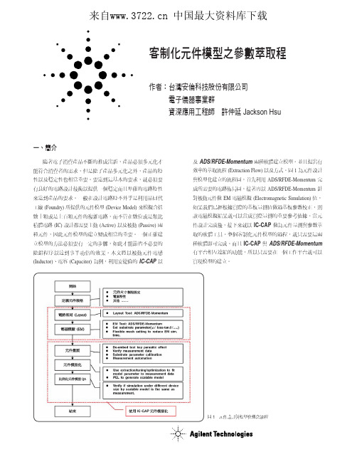
本文將以被動元件電感(Inductor)、電容(Capacitor) 為例,利用安捷倫的IC-CAP 以及ADS/RFDE-Momentum 兩種軟體建立模型。
並且提出有效率的萃取流程(Extraction Flow) 以及方式。
圖1 為元件設計與模型化建立的流程圖,首先利用ADS/RFDE-Momentum 完成所需要的電路佈局圖,接著再以ADS/RFDE-Momentum 針對被動元件做EM 電磁模擬(Electromagnetic Simulation) 值,如果我們已經根據實際的基板量測值做過基板參數校正,則該電磁模擬結果就可以當成實際量測的重要參考依據。
當元件設計完成後,接下來就以IC-CAP 做為元件量測與參數萃取的軟體工具。
整個客制化元件模型的過程,就只需要這兩種軟體即可完成。
而且IC-CAP 與ADS/RFDE-Momentum 有平台相互連結的功能,所以只需要在一個工作平台就可以實現模型的建立。
圖1元件設計與模型化概念流程二、被動元件電路佈局圖A、Substrate 特性的萃取利用ADS/RFDE-Momentum可以完成電路的佈局圖,首先開啟主視窗如圖2 所示,選定Layout 的形狀後就可以在主視窗裡完成佈局圖。
bjt_model参数解释剖析

附件A、三极管的Pspice模型参数.Model <model name> NPN(PNP、LPNP) [model parameters]第 1 页共9页第 2 页共9页附件B、PSpice Goal Function第 3 页共9页附件CModeling voltage-controlled and temperature-dependent resistorsAnalog Behavioral Modeling (ABM) can be used to model a nonlinear resistor through use of Ohm抯 law and tables and expressions which describe resistance. Here are some examples.Voltage-controlled resistorIf a Resistance vs. Voltage curve is available, a look-up table can be used in the ABM expression. This table contains (Voltage, Resistance) pairs picked from points on the curve. The voltage input is nonlinearly mapped from the voltage values in the table to the resistance values. Linear interpolation is used between table values.Let抯 say that points picked from a Resistance vs. Voltage curve are:Voltage ResistanceThe ABM expression for this is shown in Figure 1.第 4 页共9页Figure 1 - Voltage controlled resistor using look-up tableTemperature-dependent resistorA temperature-dependent resistor (or thermistor) can be modeled with a look-up table, or an expression can be used to describe how the resistance varies with temperature. The denominator in the expression in Figure 2 is used to describe common thermistors. The TEMP variable in the expression is the simulation temperature, in Celsius. This is then converted to Kelvin by adding 273.15. This step is necessary to avoid a divide by zero problem in the denominator, when T=0 C.NOTE: TEMP can only be used in ABM expressions (E, G devices).Figure 3 shows the results of a DC sweep of temperature from -40 to 60 C. The y-axis shows the resistance or V(I1:-)/1A.Figure 2 - Temperature controlled resistor第 5 页共9页Figure 3 - PSpice plot of Resistance vs. Temperature (current=1A)Variable Q RLC networkIn most circuits the value of a resistor is fixed during a simulation. While the value can be made to change for a set of simulations by using a Parametric Sweep to move through a fixed sequence of values, a voltage-controlled resistor can be made to change dynamically during a simulation. This is illustrated by the circuit shown in Figure 5, which employs a voltage-controlled resistor.第 6 页共9页Figure 4 - Parameter sweep of control voltageThis circuit employs an external reference component that is sensed. The output impedance equals the value of the control voltage times the reference. Here, we will use Rref, a 50 ohm resistor as our reference. As a result, the output impedance is seen by the circuit as a floating resistor equal to the value of V(Control) times the resistance value of Rref. In our circuit, the control voltage value is stepped from 0.5 volt to 2 volts in 0.5 volt steps, therefore, the resistance between nodes 3 and 0 varies from 25 ohms to 100 ohms in 25 ohm-steps.第7 页共9页Figure 5 - Variable Q RLC circuitA transient analysis of this circuit using a 0.5 ms wide pulse will show how the ringing differs as the Q is varied.Using Probe, we can observe how the ringing varies as the resistance changes. Figure 6 shows the input pulse and the voltage across the capacitor C1. Comparing the four output waveforms, we can see the most pronounced ringing occurs when the resistor has the lowest value and the Q is greatest. Any signal source can be used to drive the voltage-controlled resistance. If we had used a sinusoidal control source instead of a staircase, the resistance would have varied dynamically during the simulation.第8 页共9页Figure 6 - Output waveforms of variable Q RLC circuit第9 页共9页。
Multisim电路设计与仿真14第10章习题答案
第10章习题参考答案
1.答、热噪声(Thermal Noise):也就是约翰逊噪声(Johnson Noise)或白色噪声(White Noise),这种噪声敏感于温度的变化,由导体中的自由电子和振动粒子之间的热量的相互作用而产生,它的频率在频谱总均匀分布。
散粒噪声(Shot Noise):这种噪声是由各种形式半导体中载流子的分散特性而产生的,这种噪声为晶体管的主要噪声。
闪烁噪声(Flicker Noise):又称为超越噪声(Excess Noise)、粉红噪声(Pink Noise)或1/f噪声,通常由双极型晶体管(BJT)和场效应管(FET)产生,且发生在频率小于1kHz 以下。
闪烁噪声是所有线性器件固有的随机噪声,噪声振幅与频率成反比,频率很低时这种噪声较大,频率较高时(几百赫兹以上)这种噪声的影响较小。
在电路的输入端,闪烁噪声通常是频率低于400Hz时的主要噪声源。
2答:失真分析(Distortion Analysis)用于分析电子电路中的非线性失真和相位偏移,通常非线性失真会导致谐波失真,而相位偏移会导致互调失真。
3、建立10-44仿真电路
对该电路进行静态工作点分析的结果如下图10.1所示。
图10.1
对6节点进行交流分析的结果如下图10.2所示。
图10.2
对节点6进行瞬态分析的结果如下图10.3所示,其中End time(TSTOP)设置为0.1s。
图10.3。
- 1、下载文档前请自行甄别文档内容的完整性,平台不提供额外的编辑、内容补充、找答案等附加服务。
- 2、"仅部分预览"的文档,不可在线预览部分如存在完整性等问题,可反馈申请退款(可完整预览的文档不适用该条件!)。
- 3、如文档侵犯您的权益,请联系客服反馈,我们会尽快为您处理(人工客服工作时间:9:00-18:30)。
F.Sischka Agilent Technologies GmbH, Munich
modeling toolkits NOISE.DOC | 22.04.02
Franz Sischka
Noise Modeling for Semiconductors -2-
1. Introduction
Fig.1: low frequency noise spectral density current of a bipolar transistor [A2/Hz], measured at the Collector. Broadband noise in bipolar or FET models is determined essentially by thermal noise and shot noise. These noise sources are automatically determined within the model from the large signal model parameters. An important prerequisite for this is, however, that the noise determining parameters, e.g. the Base resistor of bipolar transistors, has been determined carefully and that their values have a physical meaning. The low frequency noise, on the other hand, dominated by the 1/f noise, is modeled by some specific model parameters. In general, these are the AF and KF and sometimes BF/EF parameters, covered in this chapter. With some models, like the BSIM3v3, an alternate 1/f noise model is available too [10,15].
Noise Terms Definitions
In order to keeps things simple, we consider white noise of a resistor. This frequencyindependent and bias-independent noise is described in terms of a voltage by the well-known formula
v nR 2 = 4 ⋅ k ⋅ T ⋅ ∆f ∗ R
with
v nR 2 4 ⋅ k ⋅ T ⋅ ∆f R effective noise voltage (root means square value), in [V2] this product represents a power, with dimension [A*V] resistance value
Phase noise of oscillator circuits is among the key parameters of today's communication systems. It limits the modulation quality of the information signal, and the cross-talk to adjacent channels. In the receiver, on the other hand, it can reduce the selectivity and the demodulation quality. With today's trend to even more complex modulation schemes, low phase noise becomes even more critical. Therefore, minimizing noise with the design of high frequency communications circuits is a must for the cost-effective exploitation of limited bandwidth, and to obtain low bit error rates. In order to predict the noise behavior of such systems correctly, accurate noise models are required. Without them, the design and optimization of an amplifier's noise figure or the phase noise of oscillators cannot be successful. A key element is the transistor. While for linear circuits the modeling of the noise at the operating frequency f0 is sufficient, non-linear circuits do also convert the low-frequency noise up to the operating frequency range. For oscillators as an example, the 1/f low frequency noise at fm will be mixed upwards to contribute to the phase noise of the total circuit at the frequencies f0+fm and f0-fm . Therefore, noise modeling of transistors can be split into a high and a low frequency segment. Fig.1 depicts the Collector low-frequency noise spectral density [A2/Hz] of a bipolar transistor. It can be seen that the resolution of the toolkit measurement setup is at about 0.2nA / Hz .
v nR 2 Snv = ∆f = 4 ⋅k ⋅T ∗ R
In some cases, the square root of Snv is used, called the equivalent noise voltage, Env [V/√Hz].
Env = v nR 2 ∆f
Note: using Env instead of Snv does not require to calculate noise transmissions/amplifications using squares of R, amplification etc. See below.
v nR 2 is called power noise spectral density. ∆f
However, this is not exact, referring to the dimensions. A more appropriate term is therefore voltage noise spectral density. Its symbol is usually Snv, and its dimension is [V2 / Hz]
modeling toolkits NOISE.DOC | 22.04.02
Franz Sischka
Noise Modeling for Semiconductors -4-
Note: When expressing noise in terms of currents, e.g. same terminology applies.
v nR 2 = 4 ⋅k ⋅T ∗ R ∆f
This result can be plotted against frequency. In case of our resistor, it is a constant value. For semiconductors, such a plot can also exhibit frequency dependencies, e.g. 1/f noise. In any case, such a plot shows a spectrum. Therefore, this term
modeling toolkits NOISE.DOC | 22.04.02
Franz Sischka
Noise Modeling for Semiconductors -3Since there is much confusion about noise terms, noise units etc., we will first commence with a small chapter on
Sv1
amplSv2 = Sv1源自(ampl)2RSv = Si * R2
SiC = ß2 * SiB
modeling toolkits NOISE.DOC | 22.04.02
Franz Sischka
1. Introduction 2. Types of Noise in Semiconductors 3. Noise Models in Semiconductors 4. 1/f Noise Measurement Setup 5. AF, KF and BF/EF Noise Parameter Extraction and Verification 6. Appendix: Noise floor information on the toolkit measurement setup 7. Acknowledgements and Publications