fm151A
SMF15A中文资料
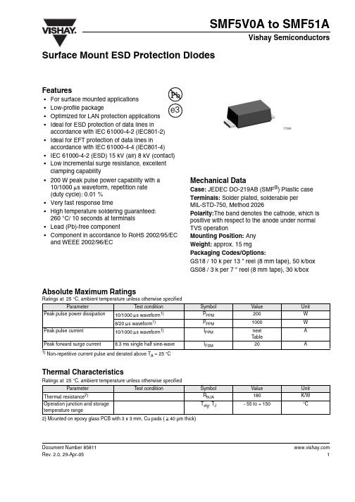
Document Number 17249Surface Mount ESD Protection DiodesFeatures•For surface mounted applications •Low-profile package•Optimized for LAN protection applications •Ideal for ESD protection of data lines in accordance with IEC 61000-4-2 (IEC801-2) •Ideal for EFT protection of data lines in accordance with IEC 61000-4-4 (IEC801-4) •IEC 61000-4-2 (ESD) 15 kV (air) 8 kV (contact) •Low incremental surge resistance, excellent clamping capability •200 W peak pulse power capability with a 10/1000 µs waveform, repetition rate (duty cycle): 0.01 % •Very fast response time•High temperature soldering guaranteed:260°C/ 10 seconds at terminals •Lead (Pb)-free component•Component in accordance to RoHS 2002/95/EC and WEEE 2002/96/ECMechanical DataCase: JEDEC DO-219AB (SMF ®) Plastic case Terminals: Solder plated, solderable per MIL-STD-750, Method 2026Polarity:The band denotes the cathode, which is positive with respect to the anode under normal TVS operationMounting Position: Any Weight: approx. 15 mgPackaging Codes/Options:GS18 / 10 k per 13 " reel (8 mm tape), 50 k/box GS08 / 3 k per 7 " reel (8 mm tape), 30 k/boxAbsolute Maximum RatingsRatings at 25°C, ambient temperature unless otherwise specified1)Non-repetitive current pulse and derated above T A = 25°CThermal CharacteristicsRatings at 25°C, ambient temperature unless otherwise specified2) Mounted on epoxy glass PCB with 3 x 3 mm, Cu pads ( ≥ 40 µm thick)ParameterT est conditionSymbol Value Unit Peak pulse power dissipation 10/1000 µs waveform 1)P PPM 200W 8/20 µs waveform 1)P PPM 1000W Peak pulse current 10/1000 µs waveform 1)I PPM next Table A Peak forward surge current8.3 ms single half sine-waveI FSM20AParameterT est conditionSymbol Value Unit Thermal resistance 2)R thJA 180K/W Operation junction and storage temperature rangeT stg , T J- 55 to + 150°C Document Number 85811Electrical CharacteristicsRatings at 25°C ambient temperature unless otherwise specified. V F = 3.5 V at I F = 12 A (uni-directional only)1) Pulse test t p≤ 5.0 ms2)Surge current waveform 10/1000 µs3) All terms and symbols are consistent with ANSI/IEEE C62.35PartnumberMarking Code UNIBreakdown Voltage 1)Test CurrentStand-off VoltageMaximum Reverse Leakage Maximum Peak Pulse Surge Current 2,3)Maximum Clamping VoltageJunction CapacitanceV (BR)@ I TV WM@ V WMI D I PPM@ I PPM V CC j @ V R = 0 V, f = 1 MHzV mA V µA AV pF mintypSMF5V0A AE 6.4010 5.040021.79.21030SMF6V0A AG 6.6710 6.040019.410.31010SMF6V5A AK 7.2210 6.525017.911.2850SMF7V0A AM 7.78107.010016.712.0750SMF7V5A AP 8.33 1.07.55015.512.9730SMF8V0A AR 8.89 1.08.02514.713.6670SMF8V5A AT 9.44 1.08.51013.914.4660SMF9V0A AV 10.0 1.09.0 5.013.515.4620SMF10A AX 11.1 1.010 2.511.817.0570SMF11A AZ 12.2 1.011 2.511.018.2460SMF12A BE 13.3 1.012 2.510.119.9440SMF13A BG 14.4 1.013 1.09.321.5420SMF14A BK 15.6 1.014 1.08.623.2370SMF15A BM 16.7 1.015 1.08.224.4350SMF16A BP 17.8 1.016 1.07.726.0340SMF17A BR 18.9 1.017 1.07.227.6310SMF18A BT 20.0 1.018 1.0 5.829.2305SMF20A BV 22.2 1.020 1.0 6.232.4207SMF22A BX 24.4 1.022 1.0 5.635.5265SMF24A BZ 26.7 1.024 1.0 5.138.9240SMF26A CE 28.9 1.026 1.0 4.842.1225SMF28A CG 31.1 1.028 1.0 4.445.4210SMF30A CK 33.3 1.030 1.0 4.148.4205SMF33A CM 36.7 1.033 1.0 3.853.3190SMF36A CP 40.0 1.036 1.0 3.458.1180SMF40A CR 44.4 1.040 1.0 3.164.5165SMF43A CT 47.8 1.043 1.0 2.969.4160SMF45A CV 50.0 1.045 1.0 2.872.7155SMF48A CX 53.3 1.048 1.0 2.677.4150SMF51ACZ56.71.0511.02.482.4145Document Number Typical Characteristics (Tamb = 25 °C unless otherwise specified)Figure 1. Peak Pulse Power RatingFigure 2. Pulse Derating CurveFigure 3. Pulse WaveformP P P M -P e a k P u l s e P o w e r (k W )0.11100.1µ s 1.0µ s 10µ s t d -Pulse Width (sec.)100µ s 1.0ms 10ms172502550751000752550100125150175200P e a k P u l s e P o w e r (P P P )o r C u r r e n t (I P P M )D e r a t i n g i n P e r c e n t a g e ,%T A -Ambient Temperature (°C)17251I P P M -P e a k P u l s e C u r r e n t ,%I R S M2.0t -Time (ms)17252Package Dimensions in mm (Inches) Document Number 85811Blistertape for SMFDocument Number Ozone Depleting Substances Policy StatementIt is the policy of Vishay Semiconductor GmbH to1.Meet all present and future national and international statutory requirements.2.Regularly and continuously improve the performance of our products, processes, distribution and operatingsystems with respect to their impact on the health and safety of our employees and the public, as well as their impact on the environment.It is particular concern to control or eliminate releases of those substances into the atmosphere which are known as ozone depleting substances (ODSs).The Montreal Protocol (1987) and its London Amendments (1990) intend to severely restrict the use of ODSs and forbid their use within the next ten years. Various national and international initiatives are pressing for an earlier ban on these substances.Vishay Semiconductor GmbH has been able to use its policy of continuous improvements to eliminate the use of ODSs listed in the following documents.1.Annex A, B and list of transitional substances of the Montreal Protocol and the London Amendmentsrespectively2.Class I and II ozone depleting substances in the Clean Air Act Amendments of 1990 by the EnvironmentalProtection Agency (EPA) in the USA3.Council Decision 88/540/EEC and 91/690/EEC Annex A, B and C (transitional substances) respectively. Vishay Semiconductor GmbH can certify that our semiconductors are not manufactured with ozone depleting substances and do not contain such substances.We reserve the right to make changes to improve technical designand may do so without further notice.Parameters can vary in different applications. All operating parameters must be validated for each customer application by the customer. Should the buyer use Vishay Semiconductors products for any unintended or unauthorized application, the buyer shall indemnify Vishay Semiconductors against all claims, costs, damages, and expenses, arising out of, directly or indirectly, any claim of personal damage, injury or death associated with such unintended or unauthorized use.Vishay Semiconductor GmbH, P.O.B. 3535, D-74025 Heilbronn, Germany Document Number 85811。
1951A中文资料
Gate
Source
Source
S-Parameter Reference Planes
Drain
MITSUBISHI
(4/4)
1 Aug 2002
Drain Current ID (mA)
60 50 40 30 20 10 0 0 1 2 3 4 -0.2V/step
60 50 40 30 20 10 0 -2.0 -1.5 -1.0 -0.5 0
Drain to Source Voltage VDS (V) OUTPUT POWER vs INPUT POWER
20
Gate to Source Voltage VGS (V)
Output Power Pout (dBm)
VDS=3V ID=30mA f=12GHz 15
10
5
0 -10
-5
0
5
10
Input Power Pin (dBm)
MITSUBISHI
(3/4)
1 Aug 2002
元器件交易网
QUALITY
General Grade
ORDERING INFORMATION
Part Number MGF1951A-01 Quantity 3.000 pcs/reel Supply Form Tape & Reel
Keep Safety first in your circuit designs!
View A
MITSUBISHI
(2/4)
1 Aug 2002
40. 55
z
C 2 4AA
x
y
y
y
±0
.0 5
2-R0.20
RFM151 有线电视射频 分析仪 说明书

RFM151有线电视射频分析仪用户手册简介RFM 151 SignalScout 是专为电缆电视应用而设计的高性能RF信号电平仪。
它不公用于电平测量,还可在电缆电视系统的安装和维护中完成其它必需的测量。
这些测量项目包括播出中的载噪比、信号交流声比、频谱显示和FM频偏。
仪器内还设有FM 检波器和扬声器。
特点电平测量方式LEVEL键(电平键)可提供电平测量的五种方式。
单频道方式(1 channel mode)可显示图象载波电平(以dBmV或dBuV 表示)、伴音载波电平差(以dBc表示)、频道号和该频道的频率。
导频方式(pilots mode)(双频道)和5频道方式(5 channel mode)可用于同时测量2个频道或5个频道的工作电平。
模拟表方式(analog meter mode)一般用作电平测量,并且带有仿模拟表头的显示。
该方式可用于峰值/零值调整。
全频道方式(all channel mode)可用图案显示由用户选择的频道表所规定的所有图象载波电平。
其它工作方式按一下MEAS键,可进行载噪比、信号交流声比和FM频偏测量,但要选择相应的测量功能。
这些测量均显示被调谐频道的图象载波电平。
SPECT键提供频谱显示。
该测量方式显示出被测频道的频谱,其分辨带宽可选为30KHZ或300KHZ,跨宽范围也可选择。
使用参考频标可测出频谱中任意点的电平和频率。
这种方式可用于频谱的细致分析以发现频道中的异常现象。
按一下SWEEP键,即可选出参考扫描。
用户可先在电缆电视系统的前面某一部位测出载波电平频响,并把结果储存下来作为参考,接着在系统后面另一部位测出频响,并将后一部位的频响与储存的前一部位的频响参考相比较。
按下HELP键,可显示出与上下有关联的求助程序屏幕(help screens)。
旋转园钮可使显示内容上下移动。
用户接口菜单键(menu keys)的栏目选择可通过功能键(F1-F5)、园钮或数字键盘获得。
芯片pn551a参数

芯片pn551a参数
PN551A芯片是一款由NXP Semiconductors推出的NFC(近场通信)芯片。
它是一款高性能的NFC解决方案,具有多种功能和特性。
首先,让我们从PN551A芯片的性能参数方面来看。
PN551A芯
片采用了NXP Semiconductors的高性能射频技术,具有优秀的无线
通信性能。
它支持ISO/IEC 14443 Type A/B、ISO/IEC 15693和FeliCa等多种NFC标准,能够实现与各种NFC设备的兼容性。
此外,PN551A芯片还具有较高的数据处理能力和安全性能,能够满足复杂
的应用需求。
其次,从功能特性方面来看,PN551A芯片具有丰富的功能。
它
支持卡模拟模式、读写器模式和点对点模式,能够实现多种NFC应
用场景下的灵活应用。
此外,PN551A芯片还内置了丰富的安全功能,包括数据加密、认证和访问控制等,能够保障通信数据的安全性。
除此之外,PN551A芯片还具有低功耗特性,能够满足移动设备
等对电池续航能力要求较高的场景。
它还支持多种封装形式,便于
在不同的应用场景中进行灵活应用。
总的来说,PN551A芯片作为一款高性能的NFC解决方案,具有丰富的功能和性能特点,能够满足各种复杂的NFC应用需求。
希望这些信息能够满足你的需求,如果你还有其他方面的问题,也欢迎继续提问。
TDA1514A中文资料
May 1992
Fig.3 SOAR protection curve. 5
元器件交易网
Philips Semiconductors
50 W high performance hi-fi amplifier
f = 100 Hz
VP
± 10
−
± 30
V
Itot
−
56
−
mA
Po
−
40
−
W
Po
−
48
−
W
Gc
−
30
−
dB
Ri
−
20
−
kΩ
(S+N)/N
−
83
−
dB
SVRR
−
64
−
dB
PACKAGE OUTLINE 9-lead SIL, plastic power (SOT131R); SOT131-2; 1996 July 19.
Considering, for example, a maximum ambient temperature of 50 °C and a maximum junction temperature of 150 °C the total thermal resistance is:
Rth j-a = 1----5---0--1---9–-----5---0-- = 5.3 K/W Since the thermal resistance of the SOT131A encapsulation is Rth j-mb < 1 K/W, the thermal resistance required of the heatsink is Rth h-a < 4.3 K/W.
FGA15N120AN中文资料

I CES Collector Cut-Off Current V CE = V CES, V GE = 0V----3mA I GES G-E Leakage Current V GE = V GES, V CE = 0V ----± 100nAOn CharacteristicsV GE(th)G-E Threshold Voltage I C = 15mA, V CE = V GE 3.5 5.57.5VV CE(sat)Collector to EmitterSaturation VoltageI C = 15A, V GE = 15V-- 2.4 3.2VI C = 15A, V GE = 15V,T C = 125°C-- 2.9--VI C = 24A, V GE = 15V-- 3.0--VDynamic CharacteristicsC ies Input Capacitance VCE = 30V, V GE = 0V,f = 1MHz --1150--pFC oes Output Capacitance--120--pF C res Reverse Transfer Capacitance--56--pFSwitching Characteristicst d(on)Turn-On Delay TimeV CC = 600 V, I C = 15A,R G = 20Ω, V GE = 15V,Inductive Load, T C = 25°C --90--nst r Rise Time--70--ns t d(off)Turn-Off Delay Time--310--ns t f Fall Time--60120ns E on Turn-On Switching Loss-- 3.27 4.9mJ E off Turn-Off Switching Loss--0.60.9mJ E ts TotalSwitchingLoss-- 3.68 5.8mJt d(on)Turn-On Delay TimeV CC = 600 V, I C = 15A,R G = 20Ω, V GE = 15V,Inductive Load, T C = 125°C --80--nst r Rise Time--60--ns t d(off)Turn-Off Delay Time--310--ns t f Fall Time--50--ns E on Turn-On Switching Loss-- 3.41--mJ E off Turn-Off Switching Loss--0.84--mJ E ts TotalSwitchingLoss-- 4.25--mJQ g Total Gate ChargeV CE = 600 V, I C = 15A,V GE = 15V --120180nCQ ge Gate-Emitter Charge--914nC Q gc Gate-Collector Charge--6395nC L e Internal Emitter Inductance Measured 5mm from PKG--14--nHFGA15N120ANDISCLAIMERFAIRCHILD SEMICONDUCTOR RESERVES THE RIGHT TO MAKE CHANGES WITHOUT FURTHER NOTICE TO ANY PRODUCTS HEREIN TO IMPROVE RELIABILITY, FUNCTION OR DESIGN. FAIRCHILD DOES NOT ASSUME ANY LIABILITY ARISING OUT OF THE APPLICATION OR USE OF ANY PRODUCT OR CIRCUIT DESCRIBED HEREIN;NEITHER DOES IT CONVEY ANY LICENSE UNDER ITS PATENT RIGHTS, NOR THE RIGHTS OF OTHERS.LIFE SUPPORT POLICYFAIRCHILD’S PRODUCTS ARE NOT AUTHORIZED FOR USE AS CRITICAL COMPONENTS IN LIFE SUPPORT DEVICES OR SYSTEMS WITHOUT THE EXPRESS WRITTEN APPROVAL OF FAIRCHILD SEMICONDUCTOR CORPORATION.As used herein:1. Life support devices or systems are devices or systems which, (a) are intended for surgical implant into the body,or (b) support or sustain life, or (c) whose failure to perform when properly used in accordance with instructions for use provided in the labeling, can be reasonably expected to result in significant injury to the user.2. A critical component is any component of a life support device or system whose failure to perform can be reasonably expected to cause the failure of the life support device or system, or to affect its safety or effectiveness.PRODUCT STATUS DEFINITIONS Definition of TermsDatasheet Identification Product Status DefinitionAdvance InformationFormative or In Design This datasheet contains the design specifications for product development. Specifications may change in any manner without notice.PreliminaryFirst ProductionThis datasheet contains preliminary data, andsupplementary data will be published at a later date.Fairchild Semiconductor reserves the right to make changes at any time without notice in order to improve design.No Identification Needed Full ProductionThis datasheet contains final specifications. Fairchild Semiconductor reserves the right to make changes at any time without notice in order to improve design.Obsolete Not In ProductionThis datasheet contains specifications on a product that has been discontinued by Fairchild semiconductor.The datasheet is printed for reference information only.TRADEMARKSThe following are registered and unregistered trademarks Fairchild Semiconductor owns or is authorized to use and is not intended to be an exhaustive list of all such trademarks.FACT Quiet Series™FAST ®FASTr™FRFET™GlobalOptoisolator™GTO™HiSeC™I 2C™ImpliedDisconnect™ISOPLANAR™LittleFET™MICROCOUPLER™MicroFET™MicroPak™MICROWIRE™MSX™MSXPro™OCX™OCXPro™OPTOLOGIC ®OPTOPLANAR™PACMAN™POP™Power247™PowerTrench ®QFET ®QS™QT Optoelectronics™Quiet Series™RapidConfigure™RapidConnect™SILENT SWITCHER ®SMART START™SPM™Stealth™SuperSOT™-3SuperSOT™-6SuperSOT™-8SyncFET™TinyLogic ®TINYOPTO™TruTranslation™UHC™UltraFET ®VCX™ACEx™ActiveArray™Bottomless™CoolFET™CROSSVOLT ™DOME™EcoSPARK™E2CMOS™EnSigna™FACT™Across the board. Around the world.™The Power Franchise™Programmable Active Droop™。
BT151中文资料_数据手册_参数
SYMBOL PARAMETER
CONDITIONS
MIN.
VDRM, VRRM Repetitive peak off-state
-
voltages
IT(AV) IT(RMS) ITSM
I2t dIT/dt IGM VGM VRGM PGM PG(AV) Tstg Tj
Average on-state current half sine wave; Tmb ≤ 109 ˚C
IL(Tj) IL(25 C) 3
BT145
2.5
2
1.5
1
0.5
0 -50
Fig.8.
0
50
100
150
Tj / C
Normalised latching current IL(Tj)/ IL(25˚C), versus junction temperature Tj.
IH(Tj) IH(25 C) 3
currents, f = 50 Hz; Tmb ≤ 109˚C.
VGT(Tj) 1.6 VGT(25 C)
BT151
1.4
1.2
1
0.8
0.6
0.4-50
0
50
100
150
Tj / C
Fig.6. Normalised gate trigger voltage VGT(Tj)/ VGT(25˚C), versus junction temperature Tj.
September 1997
3
Rev 1.200
Philips Semiconductors
Thyristors
Product specification
156FMI-A发动机的开发
156FMI-A发动机的开发宋如钢张宝欢白景升林建生(天津内燃机研究所,天津,300072)天津大学机械学院摘要本文介绍了156FMI-A发动机的开发过程,该发动机的主要特点是:采用了单轴平衡减振系统,挤流型燃烧室,采用机油冷却、自然风冷混合冷却的气缸盖,开发了全新的二次进气装置,全新设计的发动机外观。
156FMI-A发动机是在目前国内产量最大的CG125发动机基础上开发,试验表明,与普通CG发动机相比,156FMI-A发动机性能提高显著,最大功率达到8.75kW,最低燃油消耗率达到276g/kW.h。
同时,单轴平衡减振系统的减振效果明显,挤流型燃烧室明显改善了燃烧,大大降低了有害气体的排放,采用机油冷却、自然风冷混合冷却的气缸盖使得气缸盖温度更为理想,提高了发动机的可靠性;全新的发动机外观设计,彻底摆脱了原发动机的陈旧的外观,给消费者耳目一新的感受。
一.前言CG125发动机在国内长盛不衰的原因:价格低,可靠性好,维修方便。
从发动机的技术上讲,CG125发动机并不很先进,甚至可以说是落后,尤其是配气机构,CG125采用中置凸轮轴,顶置气门的布置方式,似乎完全不符合现在的OHC,DOHC的潮流,但是它却能在国内占有最大的市场,主要有两个原因,首先,CG125发动机的价格优势明显,这是因为CG125是国内最早的四冲程、顶置气门发动机,由于先入为主,该发动机的产量在国内也是最大的,因此该发动机的零部件的价格也比同类型发动机的零部件价格低。
其次,CG125发动机配气机构结构简单,可靠性好,维修方便,易于为消费者接受。
CG125发动机缺点也很明显:性能差(功率、扭矩、油耗与GS,CB125-T,CB125等相比),振动大(活塞连杆质量相对较大),外观陈旧。
二.开发目标我们决定在CG125发动机基础上开发156FMI-A发动机,156FMI-A发动机将保留CG125发动机的价格低,可靠性好,维修方便的优势,同时采用新技术使发动机功率更高,油耗更低,排放更清洁,在外观上也要摆脱老CG125发动机的束缚,给消费者一个耳目一新的感觉。
851a芯片参数
851a芯片是一种高性能的音频功率放大器芯片,常用于音频放大器和音响系统中。
以下是该芯片的主要参数:
供电电压:±12V ~ ±40V
输出功率:100W(THD+N=10%,RL=8Ω,f=1kHz)
工作温度范围:-40℃~ +85℃
输入阻抗:47kΩ
噪声电平:≤100μV
失真率:≤0.1%
频率响应范围:20Hz ~ 20kHz
封装形式:TO-220-15
851a芯片采用了多种保护电路,包括过热保护、过流保护、过压保护和欠压保护等,可以有效地保护芯片和外部设备。
该芯片还支持单电源和双电源供电,适用于不同的应用场景。
需要注意的是,851a芯片是一种高功率放大器芯片,使用时需要注意安全和稳定性。
在设计和使用电路时,应该遵循相关的规范和最佳实践,以确保设备的可靠性和安全性。
AUMP-15A中文资料
GENERAL SPECIFICATIONS
Attenuation: 1 - 2 GHz: Atten. = 0 - 10 dB min. 2 - 4 GHz: Atten. = 0 - 15 dB min. 4 - 8 GHz: Atten. = 0 - 20 dB min. Insertion Loss: 0.5 dB max. VSWR: 1.5:1 max. Impedance: 50 Ω nom. Average Power: 2 Watts max. Operating Temperature: -- 55° to +85°C Typical Performance
1 to 8 GHz / 0 to 20 dB / Ferrite / Excellent Temperature Stability / MIL-E-5400 Class 3 / SMA
AUMP-15A
NOTES: 1. Tolerance on 3 place decimals ± .020(.51) except as noted. 2. Dimensions in inches over millimeters. 3. Counter clockwise shaft rotation increases attenuation. 4. Shaft lock mtg. nut, shaft locking nut, flat washer and internal tooth lockwasher are supplied by MERRIMAC. 5. Call Merrimac for panel mount installation instructions.
04Mar96
NOTES:
1. Tolerance on 3 place decimals ±.020(.51) except as noted. 2. Dimensions in inches over millimeters. 3. Counterclockwise shaft rotation increases attenuation.
- 1、下载文档前请自行甄别文档内容的完整性,平台不提供额外的编辑、内容补充、找答案等附加服务。
- 2、"仅部分预览"的文档,不可在线预览部分如存在完整性等问题,可反馈申请退款(可完整预览的文档不适用该条件!)。
- 3、如文档侵犯您的权益,请联系客服反馈,我们会尽快为您处理(人工客服工作时间:9:00-18:30)。
07
换
通
道
信
号
输
出
V/I
I7
转
换
模块地址
C+ C-
通讯接口
V+ ห้องสมุดไป่ตู้-
工作电源
+24V
通讯接口 C+ C-V+V-工作电源
FM131A
64针欧式连 接器
滤 波
D/A 转 换
光 电 隔 离
滤 波
D/A
光
转
电
换
隔
离
+24V
微 控 +5V 器
DP 控 制 器
+5VD 收 发 器
调 压
FB351A-A
20针 连接器
图 2-2 模块的接口电路图
3.1 状态指示灯说明
本模块加电时 其面板上的状态指示灯 RDY 灯和 COM 灯 显示当前的工作和通讯状态 具 体组合状态及含义如表 3-1 所示
4
HollySys
FM151A 八路4 20mA号模拟量输出模块
FM151A 型模块是小负载型 8 路 4 20mA 模拟量输出模块 是 HollySys 公司采用目前世界上 先进的现场总线技术(ProfiBus-DP 总线)而新开发的模拟量输出模块 它的最大负载能力为 300 欧姆 适用于带 300 欧姆以下的负载 通过与配套的端子底座 FM131A 连接 构成输出 8 路 4 20mA 的 电流信号的 AO 处理单元 FM151A 作为 ProfiBus-DP 的从站通过 ProfiBus-DP 总线把采集到的信号 及相关诊断信息上传到 ProfiBus-DP 的主站 它是智能型的现场总线产品 可与其他公司系统相连 它也是构成 HollySys 公司的 MACSTM 系统的 I/O 单元的一种
1 3 5 7 9 11 13 15 17 19 21 23 25 27 29 31 33 35 37 39
奇数端子
I0+ NC I1+ NC I2+ NC I3+ NC I4+ NC I5+ NC I6+ NC I7+ NC NC NC C+ V+ 2 4 6 8 10 12 14 16 18 20 22 24 26 28 30 32 34 36 38 40
偶数端子
IO- NC I1- NC I2- NC I3- NC I4- NC I5- NC I6- NC I7- NC NC NC C- V图 3-1 接线端子定义图
说明
V+为模块供电电源的+24V V-为供电电源的地
通常 模块的工作电源由 FM131A 的四孔 针 连接器提
HollySys
2 原理说明
FM151A 的原理框图如图 2-1 所示 FM151A 模块通过与其相配的底座 FM131A 相连构成一个 完整的 AO 处理单元 它接收 ProfiBus-DP 的主站的数字信号 经过计算后输出 输出信号经过光
2
HollySys
FM151A 八路4 20mA号模拟量输出模块
表 3-1 面板指示灯 RDY 和 COM 的组合及含义
RDY COM
含义
闪 灭 模块工作正常 等待初始化或未得到正确的初始化数据 通讯未建立
或者通讯线路故障
灭 灭 未上电或模块坏
亮 亮 一切正常
3.2 底座端子接线说明
3.2.1 底座接线端子的定义
FM151A 模块与 FM131A 底座之间依靠 64 针欧式连接器连接 从而构成完整的 I/O 单元 现 场模拟量信号直接连接到 FM131A 侧边的双层端子上 双层接线端子定义如图 3-1 所示
FM151A 八路4 20mA号模拟量输出模块
4 技术指标
型号 FM151A
模块电源
供电电压 24VDC±10%
5
八路4 20mA模拟量输出模块 FM151A
供 因此 39/40 端子不接电源 C+ C-为通讯的正 负信号 C+ C-与配套底座 FM131A 的四孔 针 连接器的 DP 通讯正端 DP 通讯负
奇数端子
FM151
偶数端子
伺服放大
磁 放 触发器1 大 器 触发器2
现 场
开指令 关指令
阀位
执行器
图 5-1 FM151A 的一般使用方法
FM151A 可以与操作器串联使用 操作器作为后备操作 操作器信号输入端电阻应该小于
FM151A 的负载能力 图 5-2 为示意图
手/自动状态
固定孔
1.2 组成
FM151A 系 列 模 块 是 由 8 路 模 拟 输 出 板 FB351 系列 I/O 通用型智能处理板 FB311 系列 和外壳结构件组成 其外观如图 1-1 所示
模块正面标签夹中可以插入纸卡 纸卡上可以 写上 1 8 通道的测点名称或标识 便于工程使用 及维护 纸卡插入方式如图 1-2 所示
导向槽
FM151A
和利时
TM
MACS
8CH AO
标签夹
RDY COM
指示灯 指示灯2个 RDY灯 COM灯
图 1-1 FM151A 外观图示
HollySys
1
八路4 20mA模拟量输出模块 FM151A
V+ V0 NC 通 I0+ 道 NC I0-
26 通 道
+12V 100
GND
调压
+24V
+
+5V CH0
D/A转换
微 控 +5VD 器
NC 7 I7+ 通 道 NC
I7-
+12V 100
C+ C-
四孔插头 C+C-V+V-
FM131A
+
CH7
D/A转换
DP
控
制
+5VD
FB351A-A
FB311
3 使用说明
硬件产品手册
FM151A 八路 4 20mA 模拟量输出模块
北京和利时系统工程股份有限公司
2002年7月
在未得到北京和利时系统工程股份有限公司书面明确许可的情况下 无论出于什么目 的 均不得用任何电子或机械方法 以任何形式复制和传递本手册的任何部分 本手册内容如有更改 恕不另行通知 ©北京和利时系统工程股份有限公司 保留全部权利 MACSTM HollySys® 和利时®的字样和徽标均为北京和利时系统工程股份有限公司 的注册商标
HollySys
7
八路4 20mA模拟量输出模块 FM151A
5 工程应用举例
5.1 一般使用方法
一般 FM151A 输出的 4 20mA 信号 经过伺服放大器 产生控制指令 操纵执行器动作达 到调节作用 伺服放大输入端电阻应该小于 FM151A 的负载能力 如图 5-1 所示
FM151A RDY COM
8CH AO
HOLLYSYS
TM
MACS
插入纸卡 标签夹
纸卡 纸卡安装位图
图 1-2 FM151A 模件纸卡插入图示
1.3 特点和功能
FM151A 模块体积小 重量轻 安装灵活 FM151A 模块具备带电插拔功能 可在系统加电的情况下直接插拔本模块 不会影响本模块及 系统的正常运行 FM151A 模块能够定期检测 CPU 工作状态情况 具有看门狗定时器电路 可使模块在异常情况 下自动复位 FM151A 模块提供了模块电流过载保护 通讯线箝压保护 FM151A 支持实时的状态显示 可实时显示本模块的运行状态和通信状态 FM151A 具有带电复位自保持功能 FM151A 的最大负能力 300 欧姆 适用带小于 300 欧姆的负载
FB311
图 2-1 模块的原理框图
HollySys
3
八路4 20mA模拟量输出模块 FM151A
FM151A 的接口电路如图 2-2 所示
C+C-V+V四针插座
更新速度 10 次/秒 Max
负载能力
最大 300 @24VDC
通讯 通讯接口类型 ProfiBus-DP 协议 通讯速率 500Kbps/ 93.75Kbps/ 45.45Kbps/ 31.25Kbps/ 19.2Kbps/ 9.6Kbps 通讯与系统隔离电压 500Vrms
功率消耗 MAX 2.4W@24VDC 8 路空载
输出通道
通道数 8 路 通常推荐使用 6 路 以免模块温度过高 另 2 路备用
信号类型 4 20mA
输出精度 0.2%@25 满量程
温 漂 100ppm/
端是相通的 通常 模块的通讯线由 FM131A 的四孔 针 连接器接入 因此 37/38 端子不接线 In+表示电流信号输出正端 n 0~7 In-表示电流信号输出负端(n 0~7) NC 表示未用端子
3.2.2 模拟量输出信号的端子接线说明
FM151A 端子信号的接线要求每路信号采用两根 导线 屏蔽电缆 接到 FM131A 的端子上
3 使用说明
4
3.1 状态指示灯说明
4
3.2 底座端子接线说明
5
3.2.1 底座端子接线的定义
5
3.2.2 模拟量输出信号的端子接线说明
6
4 技术指标
7
5 工程应用举例
8
HollySys
FM151A 8 路 4 20mA 模拟量输出模块
1 FM151A 型模块的基本说明
块式I/O
1.1 简介
其它 外壳 宽×高×深=114mm×63mm×101mm 安装 遵循通用模块的安装方法,与 FM131A 模块连接 工作环境温度 0 ~45 工作湿度 5~90%相对湿度,不凝结 存储温度 -15 ~65 存储湿度 5~95%相对湿度,不凝结 防护等级 IP40 防混销位置 4