芯片datasheet---mic4420
DTM4420

1N-Channel 30-V (D-S) MOSFETFEATURES•Halogen-free•TrenchFET ® Power MOSFET•Optimized for High-Side SynchronousRectifier Operation •100 % R g Tested •100 % UIS TestedAPPLICATIONS•Notebook CPU Core - High-Side SwitchPRODUCT SUMMARYVDS (V)R DS(on) (Ω)I D (A)a Q g (Typ.)300.0089 at V GS = 10 V 13 6.8 nC0.012 at V GS = 4.5 V12Notes:a.Base on T C = 25 °C.b.Surface Mounted on 1" x 1" FR4 board.c.t = 10 s.d.Maximum under Steady State conditions is 85 °C/W.ABSOLUTE MAXIMUM RATINGS T A = 25 °C, unless otherwise notedParameterSymbol Limit Unit Drain-Source Voltage V DS 30VGate-Source VoltageV GS± 20Continuous Drain Current (T J = 150 °C)T C = 25 °C I D 13AT C = 70 °C 12T A = 25 °C 11b, c T A = 70 °C9b, c Pulsed Drain CurrentI DM 50Continuous Source-Drain Diode Current T C = 25 °C I S 3.8T A = 25 °C 2.1b, c Single Pulse Avalanche Current L = 0.1 mHI AS 22Avalanche EnergyE AS 24mJMaximum Power Dissipation T C = 25 °C P D 4.5WT C = 70 °C 2.8T A = 25 °C 2.5b, c T A = 70 °C 1.6b, c Operating Junction and Storage T emperature Range T J , T stg- 55 to 150°CTHERMAL RESISTANCE RATINGSParameterSymbol Typical Maximum Unit Maximum Junction-to-Ambient b, dt ≤ 10 s R thJA 3850°C/WMaximum Junction-to-Foot (Drain)Steady StateR thJF 22282Notes:a.Pulse test; pulse width ≤ 300 µs, duty cycle ≤ 2 %.b.Guaranteed by design, not subject to production testing.Stresses beyond those listed under “Absolute Maximum Ratings” may cause permanent damage to the device. These are stress ratings only, and functional operation of the device at these or any other conditions beyond those indicated in the operational sections of the specifications is not implied. Exposure to absolute maximum rating conditions for extended periods may affect device reliability.SPECIFICATIONS T J = 25 °C, unless otherwise notedParameter Symbol Test Conditions Min.Typ.Max.Unit StaticDrain-Source Breakdown Voltage V DS V GS = 0 V , I D = 250 µA30VV DS Temperature Coefficient ΔV DS /T J I D = 250 µA 28mV/°C V GS(th) Temperature Coefficient ΔV GS(th)/T J - 6Gate-Source Threshold Voltage V GS(th) V DS = V GS , I D = 250 µA 1.22.5V Gate-Source LeakageI GSS V DS = 0 V , V GS = ± 20 V ± 100nA Zero Gate Voltage Drain Current I DSS V DS = 30 V , V GS = 0 V 1µA V DS = 30 V , V GS = 0 V , T J = 55 °C10On-State Drain Current aI D(on)V DS ≥ 5 V , V GS = 10 V 20A Drain-Source On-State Resistance a R DS(on)V GS = 10 V , I D = 11 A 0.00770.0089ΩV GS = 4.5 V, I D = 10 A 0.00960.012Forward T ransconductance a g fsV DS = 15 V , I D = 11 A52SDynamic bInput Capacitance C iss V DS = 15 V , V GS = 0 V, f = 1 MHz 820pFOutput CapacitanceC oss 195Reverse Transfer Capacitance C rss 73Total Gate Charge Q g V DS = 15 V , V GS = 10 V , ID = 11 A 1523nC V DS = 15 V , V GS = 5 V , I D = 11 A6.810.2Gate-Source Charge Q gs 2.5Gate-Drain Charge Q gd 2.3Gate Resistance R g f = 1 MHz0.361.8 3.6ΩTurn-On Delay Time t d(on) V DD = 15 V , R L = 1.4 Ω I D ≅ 9 A, V GEN = 4.5 V , R g = 1 Ω1624ns Rise Timet r 1218Turn-Off Delay Time t d(off) 1624Fall Timet f 1020Turn-On Delay Time t d(on) V DD = 15 V , R L = 1.4 Ω I D ≅ 9 A, V GEN = 10 V , R g = 1 Ω816Rise Timet r 1020Turn-Off Delay Time t d(off) 1624Fall Timet f 815Drain-Source Body Diode Characteristics Continuous Source-Drain Diode Current I S T C = 25 °C 25A Pulse Diode Forward Current a I SM 50Body Diode VoltageV SD I S = 9 A0.8 1.2V Body Diode Reverse Recovery Time t rr I F = 9 A, dI/dt = 100 A/µs, T J = 25 °C1530ns Body Diode Reverse Recovery Charge Q rr 612nC Reverse Recovery Fall Time t a 8nsReverse Recovery Rise Timet b7Output CharacteristicsOn-Resistance vs. Drain Current and Gate VoltageGate ChargeTransfer CharacteristicsCapacitanceOn-Resistance vs. Junction Temperature3TYPICAL CHARACTERISTICS 25Source-Drain Diode Forward VoltageThreshold VoltageOn-Resistance vs. Gate-to-Source VoltageSingle Pulse Power, Junction-to-AmbientSafe Operating Area, Junction-to-Ambient45TYPICAL CHARACTERISTICS 25°C, unless otherwise noted*The power dissipation P D is based on T J(max) = 150 °C, using junction-to-case thermal resistance, and is more useful in settling the upper dissipation limit for cases where additional heatsinking is used. It is used to determine the current rating, when this rating falls below the package limit.Power Derating, Junction-to-FootPower Derating, Junction-to-AmbientTYPICAL CHARACTERISTICS 25°C, unless otherwise notedNormalized Thermal Transient Impedance, Junction-to-Foot 61DIM MILLIMETERSINCHESMin Max Min Max A 1.35 1.750.0530.069A 10.100.200.0040.008B 0.350.510.0140.020C 0.190.250.00750.010D 4.80 5.000.1890.196E 3.804.000.1500.157e 1.27 BSC0.050 BSCH 5.80 6.200.2280.244h 0.250.500.0100.020L 0.500.930.0200.037q 0°8°0°8°S0.440.640.0180.026ECN: C-06527-Rev. I, 11-Sep-06DWG: 54981A P P L I C A T I O N N O T ERECOMMENDED MINIMUM PADS FOR SO-8DisclaimerALL PROD UCT, PROD UCT SPECIFICATIONS AND D ATA ARE SUBJECT TO CHANGE WITHOUT NOTICE TO IMPROVE RELIABILITY, FUNCTION OR DESIGN OR OTHERWISE.Din-Tek Intertechnology, Inc., its affiliates, agents, and employees, and all persons acting on its or their behalf (collectively,“Din-Tek”), disclaim any and all liability for any errors, inaccuracies or incompleteness contained in any datasheet or in any other disclosure relating to any product.Din-Tek makes no warranty, representation or guarantee regarding the suitability of the products for any particular purpose or the continuing production of any product. To the maximum extent permitted by applicable law, Din-Tek disclaims (i) any and all liability arising out of the application or use of any product, (ii) any and all liability, including without limitation special, consequential or incidental damages, and (iii) any and all implied warranties, including warranties of fitness for particular purpose, non-infringement and merchantability.Statements regarding the suitability of products for certain types of applications are based on Din-Tek’s knowledge of typical requirements that are often placed on Din-Tek products in generic applications. Such statements are not binding statements about the suitability of products for a particular application. It is the customer’s responsibility to validate that a particular product with the properties described in the product specification is suitable for use in a particular application. Parameters provided in datasheets and/or specifications may vary in different applications and performance may vary over time. All operating parameters, including typical parameters, must be validated for each customer application by the customer’s technical experts. Product specifications do not expand or otherwise modify Din-Tek’s terms and conditions of purchase, including but not limited to the warranty expressed therein.Except as expressly indicated in writing, Din-Tek products are not designed for use in medical, life-saving, or life-sustaining applications or for any other application in which the failure of the Din-Tek product could result in personal injury or death. Customers using or selling Din-Tek products not expressly indicated for use in such applications do so at their own risk. Please contact authorized Din-Tek personnel to obtain written terms and conditions regarding products designed for such applications. No license, express or implied, by estoppel or otherwise, to any intellectual property rights is granted by this document or by any conduct of Din-Tek. Product names and markings noted herein may be trademarks of their respective owners.Material Category PolicyDin-Tek Intertechnology, Inc. hereby certifies that all its products that are identified as RoHS-Compliant fulfill the definitions and restrictions defined under Directive 2011/65/EU of The European P arliament and of the Council of June 8, 2011 on the restriction of the use of certain hazardous substances in electrical and electronic equipment (EEE) - recast, unless otherwise specified as non-compliant.Please note that some Din-Tek documentation may still make reference to RoHS Directive 2002/95/EC. We confirm that all the products identified as being compliant to Directive 2002/95/EC conform to Directive 2011/65/EU.Din-Tek Intertechnology, Inc. hereby certifies that all its products that are identified as Halogen-Free follow Halogen-Free requirements as per JEDEC JS709A standards. Please note that some Din-Tek documentation may still make reference to the IEC 61249-2-21 definition. We confirm that all the products identified as being compliant to IEC 61249-2-21 conform to JEDEC JS709A standards.1。
TC4421A中文数据手册(Microchip)「EasyDatasheet」
θJA
—
125
—
θJA
—
155
ቤተ መጻሕፍቲ ባይዱ
—
单位
条件
°C °C °C
°C/W °C/W
°C/W °C/W
无散热片
典型 4 层板,带有到地平面 的过孔
DS21946A_CN 第 4 页
2006 Microchip Technology Inc.
中文手册全文下载
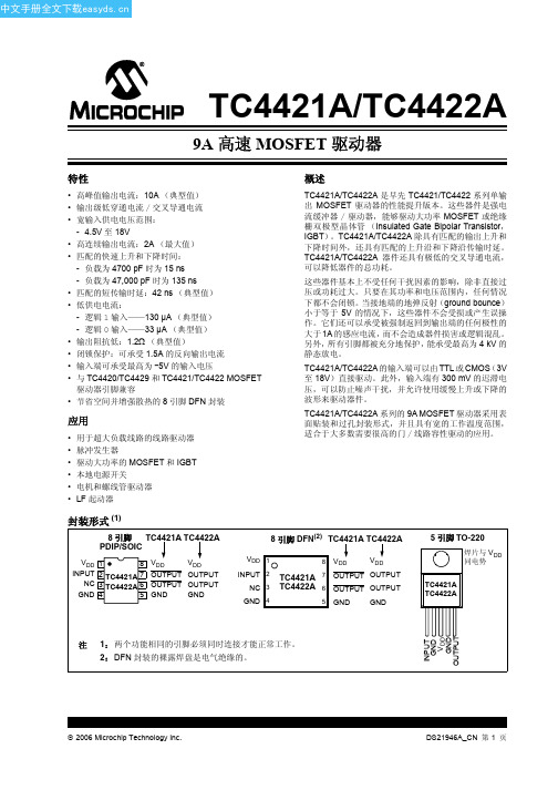
TC4421A/TC4422A
VDD 1 INPUT 2
NC 3 GND 4
8 VDD
VDD
TC4421A 7 OUTPUT OUTPUT TC4422A 6 OUTPUT OUTPUT
5 GND
GND
5 引脚 TO-220
焊片与 VDD 同电势
TC4421A TC4422A
注 1: 两个功能相同的引脚必须同时连接才能正常工作。 2: DFN 封装的裸露焊盘是电气绝缘的。
INPUT GND VDD GND
OUTPUT
2006 Microchip Technology Inc.
DS21946A_CN 第 1 页
中文手册全文下载
TC4421A/TC4422A
功能框图
输入
130 µA 300 mV
TC4421A 反相
降低交叉导通 和前驱电路
4.7V
180
160
140
22,000 pF
120
100
80
60
10,000 pF
40
20
1,000 pF 100 pF
0
4
6
8 10 12 14 16 18
Supply Voltage (V)
TC4423 datasheet

- With Logic ‘1’ Input – 3.5 mA (Max) - With Logic ‘0’ Input – 350 µA (Max) • Low Output Impedance: 3.5Ω (typ) • Latch-Up Protected: Will Withstand 1.5A Reverse Current • Logic Input Will Withstand Negative Swing Up To 5V • ESD Protected: 4 kV • Pin compatible with the TC1426/TC1427/TC1428, TC4426/TC4427/TC4428 and TC4426A/ TC4427A/TC4428A devices. • Space-saving 8-Pin 6x5 DFN Package
(Each Input)
GND
Non-inverting
4.7V TC4423 Dual Inverting TC4424 Dual Non-inverting TC4425 One Inverting, One Non-inverting
Note 1: Unused inputs should be grounded.
16-Pin SOIC (Wide) TC4423 TC4424 TC4425
NC 1 IN A 2 NC 3 GND 4 GND 5 NC 6 IN B 7 NC 8
TC4423 TC4424 TC4425
TC4429COA;TC4420COA;TC4429CPA;TC4420CPA;TC4420EPA;中文规格书,Datasheet资料
VDD Output
DS21419C-page 2
/
2004 Microchip Technology Inc.
1.0 ELECTRICAL CHARACTERISTICS
Absolute Maximum Ratings†
Supply Voltage ..................................................... +20V Input Voltage .................................. – 5V to VDD + 0.3V Input Current (VIN > VDD)................................... 50 mA Power Dissipation (TA ≤ 70°C)
- 4.5V to 18V • High Capacitive Load Drive Capability: 10,000 pF • Short Delay Time: 55 ns (typ.) • CMOS/TTL Compatible Input • Low Supply Current With Logic ‘1’ Input:
TC4420/TC4429
† Stresses above those listed under “Absolute Maximum Ratings” may cause permanent damage to the device. These are stress ratings only and functional operation of the device at these or any other conditions above those indicated in the operation sections of the specifications is not implied. Exposure to Absolute Maximum Rating conditions for extended periods may affect device reliability.
TLRO4420中文资料

12
6
www.vishay.de • FaxBack +1-408-970-5600 2 (9)
Document Number 83045 Rev. A1, 04-Feb-99
元器件交易网
TLR.442.
Vishay Telefunken
Green (TLRG4420 ) Parameter Luminous intensity Dominant wavelength Peak wavelength Angle of half intensity Forward current Breakdown voltage Junction capacitance Test Conditions VF = 12 V VF = 12 V VF = 12 V VF = 12 V VS = 12 V IR = 10 mA VR = 0, f = 1 MHz Type Symbol IV ld lp ϕ IF VBR Cj Min 1.6 562 Typ 4 565 ±30 10 70 50 Max 575 Unit mcd nm nm deg mA V pF
12
6
Soft orange (TLRO4420 ) Parameter Luminous intensity Dominant wavelength Peak wavelength Angle of half intensity Forward current Breakdown voltage Junction capacitance Test Conditions VF = 12 V VF = 12 V VF = 12 V VF = 12 V VS = 12 V IR = 10 mA VR = 0, f = 1 MHz Type Symbol IV ld lp ϕ IF VBR Cj Min 4 598 Typ 10 605 ±30 10 70 50 Max 611 Unit mcd nm nm deg mA V pF
tc4422

9A High-Speed MOSFET Drivers
Features
• High Peak Output Current: 9A • Wide Input Supply Voltage Operating Range:
- 4.5V to 18V • High Continuous Output Current: 2A Max • Fast Rise and Fall Times:
TC4421/TC4422
† Stresses above those listed under “Absolute Maximum Ratings” may cause permanent damage to the device. These are stress ratings only and functional operation of the device at these or any other conditions above those indicated in the operation sections of the specifications is not implied. Exposure to Absolute Maximum Rating conditions for extended periods may affect device reliability.
The TC4421/TC4422 inputs may be driven directly from either TTL or CMOS (3V to 18V). In addition, 300 mV of hysteresis is built into the input, providing noise immunity and allowing the device to be driven from slowly rising or falling waveforms.
mic4426
Functional DiagramVPin DescriptionPin NumberPin NamePin Function1, 8NC not internally connected2INA Control Input A: TTL/CMOS compatible logic input.3GND Ground4INB Control Input B: TTL/CMOS compatible logic input.5OUTB Output B: CMOS totem-pole output.6V S Supply Input: +4.5V to +18V 7OUTAOutput A: CMOS totem-pole output.Pin ConfigurationNC INA GND INB MIC4426Inverting MIC4426MIC4427MIC442824MIC4427Noninverting MIC4428NoninvertingOrdering InformationPart Number Temperature Range Package Configuration MIC4426AM –55°C to +125°C 8-lead SOIC Dual Inverting MIC4426BM –40°C to +85°C 8-lead SOIC Dual Inverting MIC4426BMM –40°C to +85°C 8-lead MSOP Dual Inverting MIC4426BN –40°C to +85°C 8-lead Plastic DIP Dual Inverting MIC4427AM –55°C to +125°C 8-lead SOIC Dual Noninverting MIC4427BM –40°C to +85°C 8-lead SOIC Dual Noninverting MIC4427BMM –40°C to +85°C 8-lead MSOP Dual Noninverting MIC4427BN –40°C to +85°C 8-pin Plastic DIP Dual Noninverting MIC4428AM –55°C to +125°C 8-lead SOIC Inverting + Noninverting MIC4428BM –40°C to +85°C 8-lead SOIC Inverting + Noninverting MIC4428BMM –40°C to +85°C 8-lead MSOP Inverting + Noninverting MIC4428BN–40°C to +85°C8-lead Plastic DIPInverting + NoninvertingMIC426/427/428 Device ReplacementDiscontinued NumberReplacement MIC426CM MIC4426BM MIC426BM MIC4426BM MIC426CN MIC4426BN MIC426BN MIC4426BN MIC427CM MIC4427BM MIC427BM MIC4427BM MIC427CN MIC4427BN MIC427BN MIC4427BN MIC428CM MIC4428BM MIC428BM MIC4428BM MIC428CN MIC4428BN MIC428BNMIC4428BNMIC1426/1427/1428 Device ReplacementDiscontinued NumberReplacement MIC1426CM MIC4426BM MIC1426BM MIC4426BM MIC1426CN MIC4426BN MIC1426BN MIC4426BN MIC1427CM MIC4427BM MIC1427BM MIC4427BM MIC1427CN MIC4427BN MIC1427BN MIC4427BN MIC1428CM MIC4428BM MIC1428BM MIC4428BM MIC1428CN MIC4428BN MIC1428BNMIC4428BNAbsolute Maximum Ratings (Note 1)Supply Voltage (V S)....................................................+22V Input Voltage (V IN).........................V S + 0.3V to GND – 5V Junction Temperature (T J)........................................150°C Storage Temperature...............................–65°C to +150°C Lead Temperature (10 sec.)......................................300°C ESD Rating, Note 3Operating Ratings (Note 2)Supply Voltage (V S).....................................+4.5V to +18V Temperature Range (T A)(A)........................................................–55°C to +125°C(B)..........................................................–40°C to +85°C Package Thermal ResistancePDIP θJA............................................................130°C/W PDIP θJC.............................................................42°C/W SOIC θJA...........................................................120°C/W SOIC θJC.............................................................75°C/W MSOP θJC.........................................................250°C/WElectrical Characteristics4.5V ≤ V s≤ 18V; T A = 25°C, bold values indicate full specified temperature range; unless noted.Symbol Parameter Condition Min Typ Max Units InputV IH Logic 1 Input Voltage 2.4 1.4V2.4 1.5V V IL Logic 0 Input Voltage 1.10.8V1.00.8VI IN Input Current0 ≤ V IN≤ V S–11µA OutputV OH High Output Voltage V S–0.025V V OL Low Output Voltage0.025V R O Output Resistance I OUT = 10mA, V S = 18V610Ω812ΩI PK Peak Output Current 1.5A I Latch-Up Protection withstand reverse current>500mA Switching Timet R Rise Time test Figure 11830ns2040ns t F Fall Time test Figure 11520ns2940ns t D1Delay Tlme test Flgure 11730ns1940ns t D2Delay Time test Figure 12350ns2760ns t PW Pulse Width test Figure 1400ns Power SupplyI S Power Supply Current V INA = V INB = 3.0V 1.4 4.5mA1.58mAI S Power Supply Current V INA = V INB = 0.0V0.180.4mA0.190.6mANote 1.Exceeding the absolute maximum rating may damage the device.Note 2.The device is not guaranteed to function outside its operating rating.Note 3.Devices are ESD sensitive. Handling precautions recommended.Test CircuitsINA INBFigure 2a.Noninverting Configuration90%10%10%0V 5V V S OUTPUTINPUT90%0VFigure 2b. Noninverting TimingINAINBFigure 1a.Inverting ConfigurationV OUTPUTINPUTFigure 1b.Inverting TimingElectrical CharacteristicsRise and Fall Time vs. Supply Voltage70605040100TI M E (n s )2030Delay Time vs. Supply Voltage3530252050T I M E (n s )1015-2501502550TEMPERATURE (°C)751001251010000100CAPACITIVE LOAD (pF)10001010000100CAPACITIVE LOAD (pF)1000Supply Current vs. Frequency200S U P P L Y C U R R E N T (m A )30101100010FREQUENCY (kHz)100High Output vs. Current| V – V | (V )S O U TCURRENT SOURCED (mA)Low Output vs. Current1.200.9600.480.720.24010CURRENT SUNK (mA)2030405060708090100O U T P U T V O L T A G E (V )Rise and Fall Timevs. Temperature1.200.960.480.720.240102030405060708090100-50-75Quiescent Power Supply Current vs. Supply VoltagePackage Power DissipationAMBIENT TEMPERATURE (°C)10007502500500Quiescent Power Supply 00.52.51.01.5S U P P L Y C U R R E N T (m A )SUPPLY VOLTAGE (V)2.0S U P P L Y C U R R E N T (µA )50100150200300400SUPPLY VOLTAGE (V)M A X I M U M P A C K A G EP O W E R D I S S I P A T I O N (m W )1250Applications InformationSupply BypassingLarge currents are required to charge and discharge large capacitive loads quickly. For example, changing a 1000pF load by 16V in 25ns requires 0.8A from the supply input. To guarantee low supply impedance over a wide frequency range, parallel capacitors are recommended for power sup-ply bypassing. Low-inductance ceramic MLC capacitors with short lead lengths (< 0.5") should be used. A 1.0µF film capacitor in parallel with one or two 0.1µF ceramic MLC capacitors normally provides adequate bypassing. GroundingWhen using the inverting drivers in the MIC4426 or MIC4428, individual ground returns for the input and output circuits or a ground plane are recommended for optimum switching speed. The voltage drop that occurs between the driver’s ground and the input signal ground, during normal high-current switching, will behave as negative feedback and degrade switching speed.Control InputUnused driver inputs must be connected to logic high (which can be V S) or ground. For the lowest quiescent current (<500µA) , connect unused inputs to ground. A logic-high signal will cause the driver to draw up to 9mA.The drivers are designed with 100mV of control input hyster-esis. This provides clean transitions and minimizes output stage current spikes when changing states. The control input voltage threshold is approximately 1.5V. The control input recognizes 1.5V up to V S as a logic high and draws less than 1µA within this range.The MIC4426/7/8 drives the TL494, SG1526/7, MIC38C42, TSC170 and similar switch-mode power supply integrated circuits.Power DissipationPower dissipation should be calculated to make sure that the driver is not operated beyond its thermal ratings. Quiescent power dissipation is negligible. A practical value for total power dissipation is the sum of the dissipation caused by the load and the transition power dissipation (P L + P T).Load DissipationPower dissipation caused by continuous load current (when driving a resistive load) through the driver’s output resistance is:P L = I L2 R OFor capacitive loads, the dissipation in the driver is: P L = f C L V S2Transition DissipationIn applications switching at a high frequency, transition power dissipation can be significant. This occurs during switching transitions when the P-channel and N-channel output FETs are both conducting for the brief moment when one is turning on and the other is turning off.P T = 2 f V S QCharge (Q) is read from the following graph:1×10-88×10-94×10-93×10-92×10-96×10-91×10-94681012141618SUPPLY VOLT AGE (V)CHARGE(Q)Crossover Energy Loss per TransitionPackage Information8-lead SOP (M)8-lead MM8™ MSOP (MM)0.380 (9.65)0.370 (9.40)PIN 1DIMENSIONS:INCH (MM)8-lead Plastic DIP (N)MICREL INC.1849 FORTUNE DRIVE SAN JOSE, CA95131USATEL + 1 (408) 944-0800 FAX + 1 (408) 944-0970 WEB This information is believed to be accurate and reliable, however no responsibility is assumed by Micrel for its use nor for any infringement of patents or other rights of third parties resulting from its use. No license is granted by implication or otherwise under any patent or patent right of Micrel Inc.© 1999 Micrel Incorporated。
mb202i,max202芯片资料datasheet
5 V DINROUTDOUT RS-232RIN RS-232120 kb/s15 kV HBMCopyright © 2016,Texas Instruments IncorporatedProduct FolderSample &BuyTechnical Documents Tools &SoftwareSupport &CommunityAn IMPORTANT NOTICE at the end of this data sheet addresses availability,warranty,changes,use in safety-critical applications,intellectual property matters and other important disclaimers.PRODUCTION DATA.MAX202SLLS576F –JULY 2003–REVISED SETPEMBER 2016MAX2025-V Dual RS-232Line Driver and Receiver With ±15-kV ESD Protection1Features•Meets or Exceeds the Requirements of TIA/EIA-232-F and ITU v.28Standards•ESD Protection for RS-232Bus Pins:±15-kV Human-Body Model•Operates at 5-V V CC Supply •Operates Up to 120kbit/s•Two Drivers and Two Receivers•Latch-Up Performance Exceeds 100mA Per JESD 78,Class II2Applications•Battery-Powered Systems •Notebooks •Laptops•Palmtop PCs•Hand-Held Equipment3DescriptionThe MAX202device consists of two line drivers,two line receivers,and a dual charge-pump circuit with ±15-kV ESD protection pin to pin (serial-port connection pins,including GND).The device meets the requirements of TIA/EIA-232-F and provides the electrical interface between an asynchronous communication controller and the serial-port connector.The charge pump and four small external capacitors allow operation from a single 5-V supply.The device operates at data signaling rates up to 120kbit/s and a maximum of 30-V/µs driver output slew rate.Device Information (1)PART NUMBER PACKAGE BODY SIZE (NOM)MAX202CD MAX202ID SOIC (16)9.90mm ×3.91mm MAX202CDW MAX202IDW SOIC WIDE (16)10.30mm ×7.50mm MAX202CPW MAX202IPWTSSOP (16)5.00mm x 4.40mm(1)For all available packages,see the orderable addendum atthe end of the data sheet.Block Diagram2MAX202SLLS576F –JULY 2003–REVISED SETPEMBER 2016Product Folder Links:MAX202Submit Documentation FeedbackCopyright ©2003–2016,Texas Instruments IncorporatedTable of Contents1Features ..................................................................12Applications ...........................................................13Description .............................................................14Revision History .....................................................25Pin Configuration and Functions . (36)Specifications .........................................................46.1Absolute Maximum Ratings......................................46.2ESD Ratings..............................................................46.3Recommended Operating Conditions.......................46.4Thermal Information..................................................46.5Electrical Characteristics...........................................56.6Switching Characteristics..........................................56.7Typical Characteristics .............................................67Parameter Measurement Information ..................78Detailed Description . (8)8.1Overview...................................................................88.2Functional Block Diagram.. (8)8.3Feature Description...................................................88.4Device Functional Modes (8)9Application and Implementation (10)9.1Application Information............................................109.2Typical Application.. (10)10Power Supply Recommendations .....................1311Layout . (13)11.1Layout Guidelines ................................................1311.2Layout Example. (13)12Device and Documentation Support (14)12.1Receiving Notification of Documentation Updates 1412.2Community Resources..........................................1412.3Trademarks...........................................................1412.4Electrostatic Discharge Caution............................1412.5Glossary................................................................1413Mechanical,Packaging,and OrderableInformation (14)4Revision HistoryNOTE:Page numbers for previous revisions may differ from page numbers in the current version.Changes from Revision E (April 2007)to Revision F Page•Added ESD Ratings table,Feature Description section,Device Functional Modes ,Application and Implementation section,Power Supply Recommendations section,Layout section,Device and Documentation Support section,andMechanical,Packaging,and Orderable Information section..................................................................................................1•Removed the Ordering Information table;see POA at the end of the data sheet .................................................................1•Changed values in the Thermal Information table to align with JEDEC standards (4)C1+ V CC V+ GND C1± DOUT1C2+ RIN1C2± ROUT1V ± DIN1DOUT2 DIN2RIN2ROUT23MAX202SLLS576F –JULY 2003–REVISED SETPEMBER 2016Product Folder Links:MAX202Submit Documentation FeedbackCopyright ©2003–2016,Texas Instruments Incorporated 5Pin Configuration and FunctionsD,DW,or PW Package 16-Pin SOIC or TSSOPTop ViewPin FunctionsPINI/O DESCRIPTION 1C1+—Positive lead of C1capacitor2V+O Positive charge pump output for storage capacitor only 3C1–—Negative lead of C1capacitor 4C2+—Positive lead of C2capacitor 5C2–—Negative lead of C2capacitor6V–O Negative charge pump output for storage capacitor only 7DOUT2O RS-232line data output (to remote RS-232system)8RIN2I RS-232line data input (from remote RS-232system)9ROUT2O Logic data output (to UART)10DIN2I Logic data input (from UART)11DIN1I Logic data input (from UART)12ROUT1O Logic data output (to UART)13RIN1I RS-232line data input (from remote RS-232system)14DOUT1O RS-232line data output (to remote RS-232system)15GND —Ground16V CC—Supply voltage,connect to external 5-V power supply4MAX202SLLS576F –JULY 2003–REVISED SETPEMBER 2016Product Folder Links:MAX202Submit Documentation FeedbackCopyright ©2003–2016,Texas Instruments Incorporated(1)Stresses beyond those listed under Absolute Maximum Ratings may cause permanent damage to the device.These are stress ratings only,which do not imply functional operation of the device at these or any other conditions beyond those indicated under Recommended Operating Conditions .Exposure to absolute-maximum-rated conditions for extended periods may affect device reliability.(2)All voltages are with respect to network GND.6Specifications6.1Absolute Maximum Ratingsover operating free-air temperature range (unless otherwise noted)(1)MINMAX UNIT Supply voltage,V CC (2)–0.36V Positive charge pump voltage,V+(2)V CC –0.314V Negative charge pump voltage,V–(2)–140.3V Input voltage,V I Drivers –0.3V++0.3V Receivers ±30Output voltage,V ODrivers V––0.3V++0.3VReceivers–0.3V CC +0.3Short-circuit duration,D OUTContinuousOperating junction temperature,T J 150°C Storage temperature,T stg –65150°C (1)JEDEC document JEP155states that 500-V HBM allows safe manufacturing with a standard ESD control process.(2)JEDEC document JEP157states that 250-V CDM allows safe manufacturing with a standard ESD control process.6.2ESD RatingsVALUEUNITV (ESD)Electrostatic dischargeHuman-body model (HBM),per ANSI/ESDA/JEDEC JS-001(1)Pins 7,8,13,and 14±15000V All other pins±2000Charged-device model (CDM),per JEDEC specification JESD22-C101(2)±1500(1)Test conditions are C1–C4=0.1µF at V CC =5V ±0.5V.6.3Recommended Operating Conditionsover operating free-air temperature range (unless otherwise noted (1);see Figure 10)MINNOMMAX UNIT Supply voltage4.555.5V V IH Driver high-level input voltage (D IN )2V V IL Driver low-level input voltage (D IN )0.8V V I Driver input voltage (D IN )0 5.5V Receiver input voltage –3030T A Operating free-air temperatureMAX202C 070°CMAX202I–4085(1)For more information about traditional and new thermal metrics,see the Semiconductor and IC Package Thermal Metrics application report.6.4Thermal InformationTHERMAL METRIC (1)MAX202UNITD (SOIC)DW (SOIC)PW (TSSOP)16PINS 16PINS 16PINS R θJA Junction-to-ambient thermal resistance 76.276.8101°C/W R θJC(top)Junction-to-case (top)thermal resistance 36.839.636.4°C/W R θJB Junction-to-board thermal resistance 33.941.545.9°C/W ψJT Junction-to-top characterization parameter 6.712.6 2.7°C/W ψJB Junction-to-board characterization parameter33.640.945.3°C/W5MAX202SLLS576F –JULY 2003–REVISED SETPEMBER 2016Product Folder Links:MAX202Submit Documentation FeedbackCopyright ©2003–2016,Texas Instruments Incorporated (1)Test conditions are C1–C4=0.1µF at V CC =5V ±0.5V.(2)All typical values are at V CC =5V,and T A =25°C.(3)Short-circuit durations should be controlled to prevent exceeding the device absolute power-dissipation ratings,and not more than one output should be shorted at a time.6.5Electrical Characteristicsover recommended ranges of supply voltage and operating free-air temperature (unless otherwise noted;see Figure 10)(1)PARAMETERTEST CONDITIONSMINTYP (2)MAX UNIT I CC Supply currentNo load,V CC =5V815mADRIVER SECTIONV OH High-level output voltage D OUT at R L =3k Ωto GND,D IN =GND 59V V OL Low-level output voltage D OUT at R L =3k Ωto GND,D IN =V CC –5–9V I IH High-level input current V I =V CC 0200µA I IL Low-level input current V I at 0V0–200µA I OS (3)Short-circuit output current V CC =5.5V,V O =0V±10±60mA r O Output resistance V CC ,V+,and V–=0V,V O =±2V 300ΩRECEIVER SECTIONV OH High-level output voltage I OH =–1mA 3.5V CC –0.4V V OL Low-level output voltageI OL =1.6mA 0.4V V IT+Positive-going input threshold voltage V CC =5V,T A =25°C 1.7 2.4V V IT–Negative-going input threshold voltage V CC =5V,T A =25°C0.8 1.2V V hys Input hysteresis (V IT+–V IT–)0.20.51V r i Input resistanceV I =±3V to ±25V357k Ω(1)Test conditions are C1–C4=0.1µF at V CC =5V ±0.5V.(2)All typical values are at V CC =5V,and T A =25°C.(3)Pulse skew is defined as |t PLH –t PHL |of each channel of the same device.6.6Switching Characteristicsover recommended ranges of suply voltage and operating free-air temperature (unless otherwise noted;see Figure 10)(1)PARAMETERTEST CONDITIONSMINTYP (2)MAXUNITDRIVER SECTIONMaximum data rateC L =50pF to 1000pF,R L =3k Ωto 7k ΩoneD OUT switching,see Figure 6120kbit/s t PLH(D)Propagation delay time,low-to high-level output C L =2500pF,R L =3k Ω,all drivers loaded,see Figure 62µs t PHL(D)Propagation delay time,high-to low-level output C L =2500pF,R L =3k Ω,all drivers loaded,see Figure 62µs t sk(p)Pulse skew (3)C L =150to 2500pF,R L =3k Ωto 7k Ω,see Figure 7300ns SR(tr)Slew rate,transition regionC L =50to 1000pF,R L =3k Ωto 7k Ω,V CC =5V,see Figure 63630V/µsRECEIVER SECTION (SEE Figure 8)t PLH(R)Propagation delay time,low-to high-level output C L =150pF 0.510µs t PHL(R)Propagation delay time,high-to low-level output C L =150pF 0.510µs t sk(p)Pulse skew (3)C L =150pF300ns6MAX202SLLS576F –JULY 2003–REVISED SETPEMBER 2016Product Folder Links:MAX202Submit Documentation FeedbackCopyright ©2003–2016,Texas Instruments Incorporated6.7Typical Characteristicsat T A =25°C (unless otherwise noted)TEST CIRCUITVOLTAGE WAVEFORMS50%50%–3 V3 V1.5 V1.5 VOutputInputV OL V OHt PHL (R)t PLH (R)OutputA)TEST CIRCUITVOLTAGE WAVEFORMS0 V 3 VOutputInputV OLV OHt PLH (D)t PHL (D)50%50%1.5 V1.5 VRS-232OutputA)TEST CIRCUITVOLTAGE WAVEFORMS0 V3 VOutputInputV OLV OH t PLH (D)RS-232Outputt PHL (D)A)1.5 V1.5 V3 V –3 V3 V –3 VSR(tf) =6 Vt or t PHL(D PLH(D))7MAX202SLLS576F –JULY 2003–REVISED SETPEMBER 2016Product Folder Links:MAX202Submit Documentation FeedbackCopyright ©2003–2016,Texas Instruments Incorporated 7Parameter Measurement InformationA.C L includes probe and jig capacitance.B.The pulse generator has the following characteristics:PRR =120kbit/s,Z O =50Ω,50%duty cycle,t r ≤10ns,t f ≤10ns.Figure 6.Driver Slew RateA.C L includes probe and jig capacitance.B.The pulse generator has the following characteristics:PRR =120kbit/s,Z O =50Ω,50%duty cycle,t r ≤10ns,t f ≤10ns.Figure 7.Driver Pulse SkewA.C L includes probe and jig capacitance.B.The pulse generator has the following characteristics:Z O =50Ω,50%duty cycle,t r ≤10ns,t f ≤10ns.Figure 8.Receiver Propagation Delay Times5 V DINROUTDOUT RS-232RIN RS-232120 kb/s15 kV HBMCopyright © 2016,Texas Instruments Incorporated8MAX202SLLS576F –JULY 2003–REVISED SETPEMBER 2016Product Folder Links:MAX202Submit Documentation FeedbackCopyright ©2003–2016,Texas Instruments Incorporated8Detailed Description8.1OverviewThe MAX202device is a dual driver and receiver that includes a capacitive voltage generator using four capacitors to supply TIA/EIA-232-F voltage levels from a single 5-V supply.Each receiver converts TIA/EIA-232-F inputs to 5-V TTL/CMOS levels.These receivers have shorted and open fail safe.The receiver can accept up to ±30-V inputs and decode inputs as low as ±3V.Each driver converts TTL/CMOS input levels into TIA/EIA-232-F levels.Outputs are protected against shorts to ground.8.2Functional Block Diagram8.3Feature Description8.3.1PowerThe power block increases and inverts the 5-V supply for the RS-232driver using a charge pump that requires four 0.1-µF external capacitors.8.3.2RS-232DriverTwo drivers interface standard logic levels to RS-232levels.The driver inputs do not have internal pullup resistors.Do not float the driver inputs.8.3.3RS-232ReceiverTwo Schmitt trigger receivers interface RS-232levels to standard logic levels.Each receiver has an internal 5-k Ωload to ground.An open input results in a high output on ROUT.8.4Device Functional Modes8.4.1V CC Powered by 5-VThe device is in normal operation when powered by 5V.8.4.2V CC UnpoweredWhen MAX202is unpowered,it can be safely connected to an active remote RS-232device.DIN1DOUT1RIN1ROUT1DIN2DOUT2RIN2ROUT29MAX202SLLS576F –JULY 2003–REVISED SETPEMBER 2016Product Folder Links:MAX202Submit Documentation FeedbackCopyright ©2003–2016,Texas Instruments Incorporated Device Functional Modes (continued)8.4.3Truth TablesTable 1and Table 2list the function for each driver and receiver (respectively).(1)H =high level,L =low levelTable 1.Function Table forEach Driver (1)INPUT DIN OUTPUT DOUTL H HL(1)H =high level,L =low level,Open =input disconnected or connected driver offTable 2.Function Table forEach Receiver (1)INPUT RIN OUTPUT ROUTL H H L OpenHFigure 9.Logic Diagram (Positive Logic)CBYPASS = 0.1F,m C10.1F,m 6.3 VCopyright © 2016,Texas Instruments Incorporated10MAX202SLLS576F –JULY 2003–REVISED SETPEMBER 2016Product Folder Links:MAX202Submit Documentation FeedbackCopyright ©2003–2016,Texas Instruments Incorporated9Application and ImplementationNOTEInformation in the following applications sections is not part of the TI component specification,and TI does not warrant its accuracy or completeness.TI’s customers are responsible for determining suitability of components for their purposes.Customers should validate and test their design implementation to confirm system functionality.9.1Application InformationFor proper operation,add capacitors as shown in Figure 10.Pins 9through 12connect to UART or general purpose logic lines.RS-232lines on pins 7,8,13,and 14connect to a connector or cable.9.2Typical ApplicationA.C3can be connected to V CC or GND.B.Resistor values shown are nominal.C.Nonpolarized ceramic capacitors are acceptable.If polarized tantalum or electrolytic capacitors are used,they must be connected as shown.Figure 10.Typical Operating Circuit and Capacitor Values9.2.1Design Requirements •V CC minimum is 4.5V and maximum is 5.5V.•Maximum recommended bit rate is 120kbps.RVHBM MAX202 SLLS576F–JULY2003–REVISED SETPEMBER2016 Typical Application(continued)9.2.2Detailed Design Procedure9.2.2.1Capacitor SelectionThe capacitor type used for C1through C4is not critical for proper operation.The MAX202requires0.1-µF capacitors.Capacitors up to10µF can be used without harm.Ceramic dielectrics are suggested for the0.1-µF capacitors.When using the minimum recommended capacitor values,make sure the capacitance value does not degrade excessively as the operating temperature varies.If in doubt,use capacitors with a larger(for example, 2×)nominal value.The capacitors'effective series resistance(ESR),which usually rises at low temperatures, influences the amount of ripple on V+and V–.Use larger capacitors(up to10µF)to reduce the output impedance at V+and V–.Bypass V CC to ground with at least0.1µF.In applications sensitive to power-supply noise generated by the charge pumps,decouple V CC to ground with a capacitor the same size as(or larger than)the charge-pump capacitors(C1to C4).9.2.2.2ESD ProtectionMAX202devices have standard ESD protection structures incorporated on all pins to protect against electrostatic discharges encountered during assembly and handling.In addition,the RS-232bus pins(driver outputs and receiver inputs)of these devices have an extra level of ESD protection.Advanced ESD structures were designed to successfully protect these bus pins against ESD discharge of±15-kV when powered down.9.2.2.3ESD Test ConditionsStringent ESD testing is performed by TI based on various conditions and procedures.Please contact TI for a reliability report that documents test setup,methodology,and results.9.2.2.4Human-Body Model(HBM)The HBM of ESD testing is shown in Figure11.Figure12shows the current waveform that is generated during a discharge into a low impedance.The model consists of a100-pF capacitor,charged to the ESD voltage of concern,and subsequently discharged into the device under test(DUT)through a1.5-kΩresistor.Figure11.HBM ESD Test Circuit1001502005001.51.00.50.0I -AD U T MAX202SLLS576F –JULY 2003–REVISED SETPEMBER Typical Application (continued)Figure 12.Typical HBM Current Waveform9.2.3Application Curve120kbit/s,1-nF loadFigure 13.Driver and Receiver Loopback SignalMAX202 SLLS576F–JULY2003–REVISED SETPEMBER201610Power Supply RecommendationsThe V CC voltage must be connected to the same power source used for logic device connected to DIN and ROUT pins.V CC must be between4.5V and5.5V.11Layout11.1Layout GuidelinesKeep the external capacitor traces short.This is more important on C1and C2nodes that have the fastest rise and fall times.For best ESD performance,make the impedance from MAX202ground pin to the ground plane of the circuit board as low as e wide metal and multiple vias on both sides of ground pin.11.2Layout ExampleFigure14.MAX202Circuit Board LayoutMAX202SLLS576F–JULY2003–REVISED 12Device and Documentation Support12.1Receiving Notification of Documentation UpdatesTo receive notification of documentation updates,navigate to the device product folder on .In the upper right corner,click on Alert me to register and receive a weekly digest of any product information that has changed.For change details,review the revision history included in any revised document.12.2Community ResourcesThe following links connect to TI community resources.Linked contents are provided"AS IS"by the respective contributors.They do not constitute TI specifications and do not necessarily reflect TI's views;see TI's Terms of Use.TI E2E™Online Community TI's Engineer-to-Engineer(E2E)Community.Created to foster collaboration among engineers.At ,you can ask questions,share knowledge,explore ideas and helpsolve problems with fellow engineers.Design Support TI's Design Support Quickly find helpful E2E forums along with design support tools and contact information for technical support.12.3TrademarksE2E is a trademark of Texas Instruments.All other trademarks are the property of their respective owners.12.4Electrostatic Discharge CautionThese devices have limited built-in ESD protection.The leads should be shorted together or the device placed in conductive foam during storage or handling to prevent electrostatic damage to the MOS gates.12.5GlossarySLYZ022—TI Glossary.This glossary lists and explains terms,acronyms,and definitions.13Mechanical,Packaging,and Orderable InformationThe following pages include mechanical,packaging,and orderable information.This information is the most current data available for the designated devices.This data is subject to change without notice and revision of this document.For browser-based versions of this data sheet,refer to the left-hand navigation.PACKAGING INFORMATIONAddendum-Page 1(1) The marketing status values are defined as follows:ACTIVE: Product device recommended for new designs.LIFEBUY: TI has announced that the device will be discontinued, and a lifetime-buy period is in effect.NRND: Not recommended for new designs. Device is in production to support existing customers, but TI does not recommend using this part in a new design.PREVIEW: Device has been announced but is not in production. Samples may or may not be available.OBSOLETE: TI has discontinued the production of the device.(2) Eco Plan - The planned eco-friendly classification: Pb-Free (RoHS), Pb-Free (RoHS Exempt), or Green (RoHS & no Sb/Br) - please check /productcontent for the latest availability information and additional product content details.TBD: The Pb-Free/Green conversion plan has not been defined.Pb-Free (RoHS): TI's terms "Lead-Free" or "Pb-Free" mean semiconductor products that are compatible with the current RoHS requirements for all 6 substances, including the requirement that lead not exceed 0.1% by weight in homogeneous materials. Where designed to be soldered at high temperatures, TI Pb-Free products are suitable for use in specified lead-free processes.Pb-Free (RoHS Exempt): This component has a RoHS exemption for either 1) lead-based flip-chip solder bumps used between the die and package, or 2) lead-based die adhesive used between the die and leadframe. The component is otherwise considered Pb-Free (RoHS compatible) as defined above.Green (RoHS & no Sb/Br): TI defines "Green" to mean Pb-Free (RoHS compatible), and free of Bromine (Br) and Antimony (Sb) based flame retardants (Br or Sb do not exceed 0.1% by weight in homogeneous material)(3) MSL, Peak Temp. - The Moisture Sensitivity Level rating according to the JEDEC industry standard classifications, and peak solder temperature.(4) There may be additional marking, which relates to the logo, the lot trace code information, or the environmental category on the device.Addendum-Page 2(5) Multiple Device Markings will be inside parentheses. Only one Device Marking contained in parentheses and separated by a "~" will appear on a device. If a line is indented then it is a continuation of the previous line and the two combined represent the entire Device Marking for that device.(6) Lead/Ball Finish - Orderable Devices may have multiple material finish options. Finish options are separated by a vertical ruled line. Lead/Ball Finish values may wrap to two lines if the finish value exceeds the maximum column width.Important Information and Disclaimer:The information provided on this page represents TI's knowledge and belief as of the date that it is provided. TI bases its knowledge and belief on information provided by third parties, and makes no representation or warranty as to the accuracy of such information. Efforts are underway to better integrate information from third parties. TI has taken and continues to take reasonable steps to provide representative and accurate information but may not have conducted destructive testing or chemical analysis on incoming materials and chemicals. TI and TI suppliers consider certain information to be proprietary, and thus CAS numbers and other limited information may not be available for release.In no event shall TI's liability arising out of such information exceed the total purchase price of the TI part(s) at issue in this document sold by TI to Customer on an annual basis.Addendum-Page 3TAPE AND REEL INFORMATION*All dimensions are nominal Device Package Type Package DrawingPinsSPQ Reel Diameter (mm)Reel Width W1(mm)A0(mm)B0(mm)K0(mm)P1(mm)W (mm)Pin1Quadrant MAX202CDR SOICD 162500330.016.4 6.510.3 2.18.016.0Q1MAX202CDWR SOICDW 162000330.016.410.7510.7 2.712.016.0Q1MAX202CPWR TSSOPPW 162000330.012.4 6.9 5.6 1.68.012.0Q1MAX202IDR SOICD 162500330.016.4 6.510.3 2.18.016.0Q1MAX202IDWR SOICDW 162000330.016.410.7510.7 2.712.016.0Q1MAX202IPWR TSSOP PW 162000330.012.4 6.9 5.6 1.68.012.0Q1*All dimensions are nominalDevice Package Type Package Drawing Pins SPQ Length(mm)Width(mm)Height(mm) MAX202CDR SOIC D162500333.2345.928.6 MAX202CDWR SOIC DW162000367.0367.038.0 MAX202CPWR TSSOP PW162000367.0367.035.0 MAX202IDR SOIC D162500333.2345.928.6 MAX202IDWR SOIC DW162000367.0367.038.0MAX202IPWR TSSOP PW162000367.0367.035.0IMPORTANT NOTICETexas Instruments Incorporated and its subsidiaries(TI)reserve the right to make corrections,enhancements,improvements and other changes to its semiconductor products and services per JESD46,latest issue,and to discontinue any product or service per JESD48,latest issue.Buyers should obtain the latest relevant information before placing orders and should verify that such information is current and complete.All semiconductor products(also referred to herein as“components”)are sold subject to TI’s terms and conditions of sale supplied at the time of order acknowledgment.TI warrants performance of its components to the specifications applicable at the time of sale,in accordance with the warranty in TI’s terms and conditions of sale of semiconductor products.Testing and other quality control techniques are used to the extent TI deems necessary to support this warranty.Except where mandated by applicable law,testing of all parameters of each component is not necessarily performed.TI assumes no liability for applications assistance or the design of Buyers’products.Buyers are responsible for their products and applications using TI components.To minimize the risks associated with Buyers’products and applications,Buyers should provide adequate design and operating safeguards.TI does not warrant or represent that any license,either express or implied,is granted under any patent right,copyright,mask work right,or other intellectual property right relating to any combination,machine,or process in which TI components or services are rmation published by TI regarding third-party products or services does not constitute a license to use such products or services or a warranty or endorsement e of such information may require a license from a third party under the patents or other intellectual property of the third party,or a license from TI under the patents or other intellectual property of TI.Reproduction of significant portions of TI information in TI data books or data sheets is permissible only if reproduction is without alteration and is accompanied by all associated warranties,conditions,limitations,and notices.TI is not responsible or liable for such altered rmation of third parties may be subject to additional restrictions.Resale of TI components or services with statements different from or beyond the parameters stated by TI for that component or service voids all express and any implied warranties for the associated TI component or service and is an unfair and deceptive business practice. TI is not responsible or liable for any such statements.Buyer acknowledges and agrees that it is solely responsible for compliance with all legal,regulatory and safety-related requirements concerning its products,and any use of TI components in its applications,notwithstanding any applications-related information or support that may be provided by TI.Buyer represents and agrees that it has all the necessary expertise to create and implement safeguards which anticipate dangerous consequences of failures,monitor failures and their consequences,lessen the likelihood of failures that might cause harm and take appropriate remedial actions.Buyer will fully indemnify TI and its representatives against any damages arising out of the use of any TI components in safety-critical applications.In some cases,TI components may be promoted specifically to facilitate safety-related applications.With such components,TI’s goal is to help enable customers to design and create their own end-product solutions that meet applicable functional safety standards and requirements.Nonetheless,such components are subject to these terms.No TI components are authorized for use in FDA Class III(or similar life-critical medical equipment)unless authorized officers of the parties have executed a special agreement specifically governing such use.Only those TI components which TI has specifically designated as military grade or“enhanced plastic”are designed and intended for use in military/aerospace applications or environments.Buyer acknowledges and agrees that any military or aerospace use of TI components which have not been so designated is solely at the Buyer's risk,and that Buyer is solely responsible for compliance with all legal and regulatory requirements in connection with such use.TI has specifically designated certain components as meeting ISO/TS16949requirements,mainly for automotive use.In any case of use of non-designated products,TI will not be responsible for any failure to meet ISO/TS16949.Products ApplicationsAudio /audio Automotive and Transportation /automotiveAmplifiers Communications and Telecom /communicationsData Converters Computers and Peripherals /computersDLP®Products Consumer Electronics /consumer-appsDSP Energy and Lighting /energyClocks and Timers /clocks Industrial /industrialInterface Medical /medicalLogic Security /securityPower Mgmt Space,Avionics and Defense /space-avionics-defense Microcontrollers Video and Imaging /videoRFID OMAP Applications Processors /omap TI E2E Community Wireless Connectivity /wirelessconnectivityMailing Address:Texas Instruments,Post Office Box655303,Dallas,Texas75265Copyright©2016,Texas Instruments Incorporated。
- 1、下载文档前请自行甄别文档内容的完整性,平台不提供额外的编辑、内容补充、找答案等附加服务。
- 2、"仅部分预览"的文档,不可在线预览部分如存在完整性等问题,可反馈申请退款(可完整预览的文档不适用该条件!)。
- 3、如文档侵犯您的权益,请联系客服反馈,我们会尽快为您处理(人工客服工作时间:9:00-18:30)。
Electrical Characteristics: (T A = 25°C with 4.5V ≤ V S ≤ 18V unless otherwise specified.)Symbol ParameterConditionsMinTypMaxUnitsINPUT V IH Logic 1 Input Voltage 2.41.4V V IL Logic 0 Input Voltage 1.10.8V V IN Input Voltage Range –5V S + 0.3V I IN Input Current0 V ≤ V IN ≤ V S–1010µAOUTPUT V OH High Output Voltage See Figure 1V S –0.025V V OL Low Output Voltage See Figure 10.025V R O Output Resistance,I OUT = 10 mA, V S = 18 V 1.7 2.8ΩOutput Low R O Output Resistance,I OUT = 10 mA, V S = 18 V 1.5 2.5ΩOutput High I PK Peak Output Current V S = 18 V (See Figure 5)6A I RLatch-Up Protection>500mAWithstand Reverse CurrentSWITCHING TIME (Note 3)t R Rise Time Test Figure 1, C L = 2500 pF 1235ns t F Fall Time Test Figure 1, C L = 2500 pF 1335ns t D1Delay Time Test Figure 11875ns t D2Delay TimeTest Figure 14875nsPOWER SUPPLYI S Power Supply Current V IN = 3 V 0.45 1.5mA V IN = 0 V90150µA V SOperating Input Voltage4.518VAbsolute Maximum Ratings (Notes 1, 2 and 3)Supply Voltage (20V)Input Voltage...............................V S + 0.3V to GND – 5V Input Current (V IN > V S ).........................................50mA Power Dissipation, T A ≤ 25°CPDIP...................................................................960W SOIC .............................................................1040mW 5-Pin TO-220..........................................................2W Power Dissipation, T C ≤ 25°C5-Pin TO-220.....................................................12.5W Derating Factors (to Ambient)PDIP............................................................7.7mW/°C SOIC ...........................................................8.3mW/°C 5-Pin TO-220................................................17mW/°C Storage Temperature............................–65°C to +150°C Lead Temperature (10 sec.)..................................300°COperating RatingsJunction Temperature............................................150°C Ambient TemperatureC Version ................................................0°C to +70°C B Version.............................................–40°C to +85°C Package Thermal Resistance5-pin TO-220 (θJC )..........................................10°C/W 8-pin MSOP (θJA )..........................................250°C/W查询"MIC4420"供应商where:I H =quiescent current with input high I L =quiescent current with input lowD =fraction of time input is high (duty cycle)V S =power supply voltageTransition Power DissipationTransition power is dissipated in the driver each time its output changes state, because during the transition, for a very brief interval, both the N- and P-channel MOSFETs in the output totem-pole are ON simultaneously, and a current is conducted through them from V +S to ground. The transi-tion power dissipation is approximately:P T = 2 f V S (A•s)where (A•s) is a time-current factor derived from the typical characteristic curves.Total power (P D ) then, as previously described is:P D = P L + P Q +P TDefinitionsC L =Load Capacitance in Farads.D =Duty Cycle expressed as the fraction of time theinput to the driver is high.f =Operating Frequency of the driver in Hertz I H =Power supply current drawn by a driver whenboth inputs are high and neither output is loaded.I L =Power supply current drawn by a driver whenboth inputs are low and neither output is loaded.I D =Output current from a driver in Amps.P D =Total power dissipated in a driver in Watts.P L =Power dissipated in the driver due to the driver’sload in Watts.P Q =Power dissipated in a quiescent driver in Watts.P T =Power dissipated in a driver when the outputchanges states (“shoot-through current”) in Watts.NOTE: The “shoot-through” current from a dual transition (once up, once down) for both drivers is shown by the "Typical Characteristic Curve :Crossover Area vs. Supply Voltage and is in ampere-seconds. This figure must be multiplied by the number of repetitions per second (fre-quency) to find Watts.R O =Output resistance of a driver in Ohms.V S =Power supply voltage to the IC in Volts.Capacitive Load Power DissipationDissipation caused by a capacitive load is simply the energy placed in, or removed from, the load capacitance by the driver. The energy stored in a capacitor is described by the equation:E = 1/2 C V 2As this energy is lost in the driver each time the load is charged or discharged, for power dissipation calculations the 1/2 is removed. This equation also shows that it is good practice not to place more voltage on the capacitor than is necessary, as dissipation increases as the square of the voltage applied to the capacitor. For a driver with a capaci-tive load:P L = f C (V S )2where:f =Operating Frequency C =Load Capacitance V S =Driver Supply Voltage Inductive Load Power DissipationFor inductive loads the situation is more complicated. For the part of the cycle in which the driver is actively forcing current into the inductor, the situation is the same as it is in the resistive case:P L1 = I 2 R O DHowever, in this instance the R O required may be either the on resistance of the driver when its output is in the high state, or its on resistance when the driver is in the low state,depending on how the inductor is connected, and this is still only half the story. For the part of the cycle when the inductor is forcing current through the driver, dissipation is best described asP L2 = I V D (1-D)where V D is the forward drop of the clamp diode in the driver (generally around 0.7V). The two parts of the load dissipa-tion must be summed in to produce P LP L = P L1 + P L2Quiescent Power DissipationQuiescent power dissipation (P Q , as described in the input section) depends on whether the input is high or low. A low input will result in a maximum current drain (per driver) of ≤0.2mA; a logic high will result in a current drain of ≤2.0mA.Quiescent power can therefore be found from:P Q = V S [D I H + (1-D) I L ]查询"MIC4420"供应商。