开关电源品质控制计划中英文版
制程过程IPQC检验控制计划中英文版

100%
全检 All inspection 2H 全检 All inspection
2PCS
4
装配灯罩,锁灯 罩扣位片,涂 704 硅胶(水泥 电阻)Assembly of chimney, chimney screw slice, with 704 silica gel (cement resistor)
2PCS
2H
IPQC 抽检 spot check
2
组装水窗(右) Assemble the water window
外观 appearance
100%
All inspection
操作员自检 The operator self-inspection
burst/white/screen printing is bad
制程过程 IPQC 检验控制计划中英文版
机种: type of machine number Process: KETTLE MODEL NO.: XXX sampling standard 抽样方案:GB/T2828.1-2003 AQL:Crit=(A)0 Maj=(B)1.0 Min(C)2.5
100%
全检 All inspection
2PCS
2H
PQC 抽检记录
7
装配蒸气管及锁 电制螺丝 Steam pipe assembly 夹具 fixed screws and lock the electric system
外观 appearance
1.电制组装线要牢固,螺丝要打紧/不可滑牙 目測 /漏打/用错螺丝。Electrical system eyeballing assembly line wants firm, screws are matter/non slip teeth/play/using the wrong screw. 2.蒸汽硅胶 目測 要装到位, 不能有漏装。 2. Steam silica gel eyeballing pack in place, there can be no packing. 1.电制组装插线要到位,不能松脱, 目測 Electrical system assembly line is in eyeballing place, not loose 2.锁水泥电 阻固定夹要打紧/不可有松动/螺丝未打紧/ 螺丝滑牙等现象。 Cement resistance clamp 目測 lock to matter/not have loose not eyeballing matter/screws/screw the phenomenon such
德力西 CDKU-S系列超薄型开关电源 英文说明书

CDKU-S200-350 Ultra-Thin Switching Power SupplyUser ManualStandard: Q/DLX 173 □ Please read the product instructions carefully before the installation and operation of the product, and keep those instructions properly for reference later1.Features and PurposesCDKU-S series product is a single group output enclosed switching power supply with 30mm ultra-thin appearance design, and the whole series of products use new technology, significantly reducing no-load power consumption and improving product efficiency, with efficiency up to 90%. It can be widely used in many fields such as communications, LED display, industrial control, radio and television, computer networks, medical apparatus and instruments, and intelligent monitoring.2.Product Model and Specifications and MeaningsOutput voltage codeRated capacitySingle group outputUltra-slim switching power supplyEnterprise code3. Working Conditions and Installation Method3.1 Working Conditions:Ambient temperature: -10°C~+60°C (refer to output derating curve, Fig. 1), ambient humidity: 20%~90 %Rh without condensation.3.2 Installation Method:Choose a suitable fixing position, and confirm the length and torque of the screws during installation to ensure good insulation and stability.3.3 In order to prolong the life of the equipment, please fully consider the heat dissipation problem:⚫The power supply should be installed in a place where the surrounding air is well ventilated. ⚫It is recommended to install it on a metal plate.⚫It is recommended that the spacing between the two power supplies is 20mm and more.⚫It is recommended that forced air cooling is used (such as: axial fans).4. Working PrincipleThe switching power supply is used to control the switch tube through the circuit for high-speed turn-on and turn-off, thus generating required one set or multiple sets of voltage in the secondary stage of the switching transformer.5. Use Method and Precautions5.1 Please check the wiring mark carefully before using the product, and confirm whether the input voltage meets the requirements. The meanings of the product wiring mark diagram are described as follows: "L": Phase line; "N": Zero line; " ": Earth wire; "-V": Negative voltage; "+V": Positive voltage; "COM": Output common terminal; "VADJ": Output voltage regulation.Note: For a power supply with high power, there are multiple terminals at the output terminal, and the terminal block is connected inside (equivalent to a power supply) and shall be evenly connected to the load.5.2 I n order to ensure the use safety and reduce interference, the wire that meets the electrician’s requirements must be earthed reliably when installation.5.3 There is high voltage in the machine, so that the non-professionals are prohibited to open the shell, otherwise it may cause electric shock or damage to the product.5.4 When used at different ambient temperatures, the load rate of the product should refer to "Fig. 1: Output Derating Curve Chart".5.5 When used under the different input voltages, the load rate of the product should refer to "Fig. 2 and Fig. 3 Output Derating Curve Chart". (Fig. 2 is suitable for switch selective type switching power supply, and Fig. 3 is suitable for full-range switching power supply);Fig. 1 Output Derating CurveAmbient temp. (℃)Fig. 2 Output Derating Curve (Switch Selection)Input voltage (VAC) 50Hz/60HzFig. 3 Output Derating Curve (Full Range)Input voltage (VAC) 50Hz/60HzL o a d r a t e (%)L o a d (%) L o a d (%)Note 1: 85-132/170-264VAC is optionalNote 2: Function A: Overload (overcurrent) short circuit protection; B: Output overvoltage protection; C: Over temperature protection;Selection method: F: Full range; S: Switch selection. D: Automatic on/off control of cooling fan (prolonged life); K: Output LED display.5.6 Definition of Terminal PinsCDKU-S200-3506. Transportation and StorageThe product shall not be subject to violent collisions and vibrations during transportation and storage, and shall be free from rain and snow erosion and direct sunlight.Storage temperature: -20°C~~+85°C; humidity: 10%~95%RH without condensation.8. Outline StructureFig. F1: Fig. F2:9. Description of Common Icons and SymbolsSymbol DescriptionOnly suitable for safe use in non-tropical climatesOnly suitable for safe use at the 2000m and below altitudeCaution! SafetyFor indoor use onlyEarthedACDCHigh voltage hazards! Danger! electric shockWarning!This produce is a Class A product. This product may cause radio interference in a living environment, so that it is required to take practicable measures against the interference by users in those cases.Company’s CommitmentsThe “Three-Warranty” servi ce will be provided by the company for abnormal operation of the product manufactured by our company due to poor manufacturing quality within 24 months from the date of the production under the premise that the user conforms to the storage, transportation, maintenance and operation conditions. However, the paid repair is provided for damage caused by one of the following situations even within the warranty period:1)Improper operation, maintenance, or storage;2)Modification without permission, or improper repair;3)Damage caused by falling off after purchase or occurred during the installation process;4)Irresistible nature disasters such as earthquakes, fires, lightning strikes, abnormal voltages, and secondary disaster.If you have any questions, please contact the dealer or the company’s customer service department. Customer service hotline: 400-826-8008Zhejiang DELIXI Electrical Co., Ltd.Address: No. 155, Zhenzhan East Road, Liush Town, Yueqing City, Zhejiang Province 325604 Tel: (86-577)6177 8888Fax: (86-577)6177 8000Customer service hotline: 400-826-8008The first edition of this User Manual was issued in May 2021.。
SMT控制计划 中英文
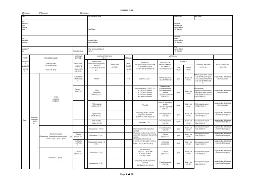
PartNumber/L atest Change LevelCore TeamCustomer Engineering Approval/Dat e (If Req'd.)PartName/De scriptionSupplier/Plant Approval/DateCustomer QualityApproval/Dat e (If Req'd.)Supplier/P lantSupplier Code Other Approval/Date (If Req'd.)OtherApproval/Dat e (If Req'd.)MACHINE,PART/DEVICE,SPECIAL PROCESS JIG,TOOLS,CHAR.SAMPLENUMBER FOR MFG.NO .CLASS (流程编号)(机器/设备/工装夹具)(特殊特性)EDS3000D (ROHS 测试仪)ROHS ▽S lead-free (无铅)ROHS inspection (进行ROHS 检测)5pcsEvery Lot (每批)ROHS report from vendor IQA ROHS test report (供应商提供的ROHS 报告 & IQA ROHS 检测报告)separate the defect Lot/inform supplierCaliper (游标卡尺)PCB Dimension (PCB 的尺寸)▽Key dimension (关键尺寸):1.1.651+/-0.100mm2. 1.778+/-0.100mm3. 3.175+/-0.100mm4.0.508+/-0.050mmMeasurement Visual Inspection CPK Report fromVendor(查看供应商提供的CPK 报告)5pcsEvery Lot (每批)IQA test dataInspection criteria status CPK Report from Vendor (IQA 检测报告 & 供应商提供的CPK 报告)separate the defect Lot/inform supplierPCB material (PCB 的材质)FR-4-86material report fromvendor(查看供应提供的材质报告)onceEvery Lot (每批) PCB material report (PCB 材质报告)separate the defect Lot/inform supplierAppearance (PCB 的外观)According to IPC-A-610E inspection standard(根据IPC-A-610E 检验标准)Visual Inspection (目视检验)5pcsEvery Lot (每批)IQA inspection report (IQA 检测报告)separate the defect Lot/inform SQE disposal PCB Validity (PCB 的有效期)one year (一年)Visual Inspection (目视检验)100%Every Lot (每批)IQA inspection report (IQA 检测报告)separate the defect Lot/inform SQE disposal Appearance (外观)Visual Inspection (目视检验)5pcsEvery Lot (每批)IQA inspection report (IQA 检测报告)separate the defect Lot/inform SQE disposal Caliper (游标卡尺) Dimension (尺寸)Caliper (游标卡尺)5pcsEvery Lot (每批)IQA inspection report (IQA 检测报告)separate the defect Lot/inform SQE disposal LCR meter (LCR 测试仪)Characteristic Value (特性值)LCR meter (LCR 测试仪)5pcsEvery Lot (每批)IQA inspection report (IQA 检测报告)separate the defect Lot/inform SQE disposalCaliper (游标卡尺)Dimension (尺寸)Key dimension(关键尺寸,参考CER ):1. 21.1+/-0.2mm2. 8.0+/-0.2mm Caliper (游标卡尺)5pcsEvery Lot (每批)IQA inspection report (IQA 检测报告)separate the defect Lot/inform SQE disposalAppearance (外观)According to IQA inspectionstandard根据IQA 的来料检验标准Visual Inspection (目视检验)5pcsEvery Lot (每批)IQA inspection report (IQA 检测报告)separate the defect Lot/inform SQE disposalStep 1Incoming Inspection (来料检验)Connector (连接器)PCB materials (PCB 物料)Electron material(Resistance ,Capacitance,Inductance ) (电子物料:电阻,电容,电感)CONTROL METHOD(控制方法)SIZE (数量)FREQ (频率)CHARACTERISTICS(特性)METHODSPart NumberReference DesignationProduct(产品特性/参考设计图纸)PROCESS NAME/(流程名称/描述)OPERATION DESCRIPTION PROCESS (过程特性)EVALUATION MEASUREMENT TECHNIQUE (评估测量的方法)REACTION PLAN (反应计划)PRODUCTPROCESS SPECIFICATIONTOLERANCE (mm)(产品&过程特性的规格要求)1.According to IQA inspection standard2.Supplier must provide COC to us by lot to make sure the autority channel.1.根据IQA 的来料检验标准2. 供应商必须提供COC 文件给到Ryder ,保证正规的供货渠道PartNumber/L atest Change LevelCore TeamCustomer Engineering Approval/Dat e (If Req'd.)PartName/De scriptionSupplier/Plant Approval/DateCustomer QualityApproval/Dat e (If Req'd.)Supplier/P lantSupplier Code Other Approval/Date (If Req'd.)OtherApproval/Dat e (If Req'd.)MACHINE,PART/DEVICE,SPECIAL PROCESS JIG,TOOLS,CHAR.SAMPLENUMBER FOR MFG.NO .CLASS (流程编号)(机器/设备/工装夹具)(特殊特性)CONTROL METHOD(控制方法)SIZE (数量)FREQ (频率)CHARACTERISTICS(特性)METHODSPart NumberReference DesignationProduct(产品特性/参考设计图纸)PROCESS NAME/(流程名称/描述)OPERATION DESCRIPTION PROCESS (过程特性)EVALUATION MEASUREMENT TECHNIQUE (评估测量的方法)REACTION PLAN (反应计划)PRODUCTPROCESS SPECIFICATIONTOLERANCE (mm)(产品&过程特性的规格要求)aph(温湿度计)(存储)(环境监督)PartNumber/L atest Change LevelCore TeamCustomer Engineering Approval/Dat e (If Req'd.)PartName/De scriptionSupplier/Plant Approval/DateCustomer QualityApproval/Dat e (If Req'd.)Supplier/P lantSupplier Code Other Approval/Date (If Req'd.)OtherApproval/Dat e (If Req'd.)MACHINE,PART/DEVICE,SPECIAL PROCESS JIG,TOOLS,CHAR.SAMPLENUMBER FOR MFG.NO .CLASS (流程编号)(机器/设备/工装夹具)(特殊特性)CONTROL METHOD(控制方法)SIZE (数量)FREQ (频率)CHARACTERISTICS(特性)METHODSPart NumberReference DesignationProduct(产品特性/参考设计图纸)PROCESS NAME/(流程名称/描述)OPERATION DESCRIPTION PROCESS (过程特性)EVALUATION MEASUREMENT TECHNIQUE (评估测量的方法)REACTION PLAN (反应计划)PRODUCTPROCESS SPECIFICATIONTOLERANCE (mm)(产品&过程特性的规格要求)PartNumber/L atest Change LevelCore TeamCustomer Engineering Approval/Dat e (If Req'd.)PartName/De scriptionSupplier/Plant Approval/DateCustomer QualityApproval/Dat e (If Req'd.)Supplier/P lantSupplier Code Other Approval/Date (If Req'd.)OtherApproval/Dat e (If Req'd.)MACHINE,PART/DEVICE,SPECIAL PROCESS JIG,TOOLS,CHAR.SAMPLENUMBER FOR MFG.NO .CLASS (流程编号)(机器/设备/工装夹具)(特殊特性)CONTROL METHOD(控制方法)SIZE (数量)FREQ (频率)CHARACTERISTICS(特性)METHODSPart NumberReference DesignationProduct(产品特性/参考设计图纸)PROCESS NAME/(流程名称/描述)OPERATION DESCRIPTION PROCESS (过程特性)EVALUATION MEASUREMENT TECHNIQUE (评估测量的方法)REACTION PLAN (反应计划)PRODUCTPROCESS SPECIFICATIONTOLERANCE (mm)(产品&过程特性的规格要求)(存储)Loading (上板架)PartNumber/L atest Change LevelCore TeamCustomer Engineering Approval/Dat e (If Req'd.)PartName/De scriptionSupplier/Plant Approval/DateCustomer QualityApproval/Dat e (If Req'd.)Supplier/P lantSupplier Code Other Approval/Date (If Req'd.)OtherApproval/Dat e (If Req'd.)MACHINE,PART/DEVICE,SPECIAL PROCESS JIG,TOOLS,CHAR.SAMPLENUMBER FOR MFG.NO .CLASS (流程编号)(机器/设备/工装夹具)(特殊特性)CONTROL METHOD(控制方法)SIZE (数量)FREQ (频率)CHARACTERISTICS(特性)METHODSPart NumberReference DesignationProduct(产品特性/参考设计图纸)PROCESS NAME/(流程名称/描述)OPERATION DESCRIPTION PROCESS (过程特性)EVALUATION MEASUREMENT TECHNIQUE (评估测量的方法)REACTION PLAN (反应计划)PRODUCTPROCESS SPECIFICATIONTOLERANCE (mm)(产品&过程特性的规格要求)PartNumber/L atest Change LevelCore TeamCustomer Engineering Approval/Dat e (If Req'd.)PartName/De scriptionSupplier/Plant Approval/DateCustomer QualityApproval/Dat e (If Req'd.)Supplier/P lantSupplier Code Other Approval/Date (If Req'd.)OtherApproval/Dat e (If Req'd.)MACHINE,PART/DEVICE,SPECIAL PROCESS JIG,TOOLS,CHAR.SAMPLENUMBER FOR MFG.NO .CLASS (流程编号)(机器/设备/工装夹具)(特殊特性)CONTROL METHOD(控制方法)SIZE (数量)FREQ (频率)CHARACTERISTICS(特性)METHODSPart NumberReference DesignationProduct(产品特性/参考设计图纸)PROCESS NAME/(流程名称/描述)OPERATION DESCRIPTION PROCESS (过程特性)EVALUATION MEASUREMENT TECHNIQUE (评估测量的方法)REACTION PLAN (反应计划)PRODUCTPROCESS SPECIFICATIONTOLERANCE (mm)(产品&过程特性的规格要求)(印刷BOT 面,Line2)PartNumber/L atest Change LevelCore TeamCustomer Engineering Approval/Dat e (If Req'd.)PartName/De scriptionSupplier/Plant Approval/DateCustomer QualityApproval/Dat e (If Req'd.)Supplier/P lantSupplier Code Other Approval/Date (If Req'd.)OtherApproval/Dat e (If Req'd.)MACHINE,PART/DEVICE,SPECIAL PROCESS JIG,TOOLS,CHAR.SAMPLENUMBER FOR MFG.NO .CLASS (流程编号)(机器/设备/工装夹具)(特殊特性)CONTROL METHOD(控制方法)SIZE (数量)FREQ (频率)CHARACTERISTICS(特性)METHODSPart NumberReference DesignationProduct(产品特性/参考设计图纸)PROCESS NAME/(流程名称/描述)OPERATION DESCRIPTION PROCESS (过程特性)EVALUATION MEASUREMENT TECHNIQUE (评估测量的方法)REACTION PLAN (反应计划)PRODUCTPROCESS SPECIFICATIONTOLERANCE (mm)(产品&过程特性的规格要求)Step 6Print(BOT)Line2PartNumber/L atest Change LevelCore TeamCustomer Engineering Approval/Dat e (If Req'd.)PartName/De scriptionSupplier/Plant Approval/DateCustomer QualityApproval/Dat e (If Req'd.)Supplier/P lantSupplier Code Other Approval/Date (If Req'd.)OtherApproval/Dat e (If Req'd.)MACHINE,PART/DEVICE,SPECIAL PROCESS JIG,TOOLS,CHAR.SAMPLENUMBER FOR MFG.NO .CLASS (流程编号)(机器/设备/工装夹具)(特殊特性)CONTROL METHOD(控制方法)SIZE (数量)FREQ (频率)CHARACTERISTICS(特性)METHODSPart NumberReference DesignationProduct(产品特性/参考设计图纸)PROCESS NAME/(流程名称/描述)OPERATION DESCRIPTION PROCESS (过程特性)EVALUATION MEASUREMENT TECHNIQUE (评估测量的方法)REACTION PLAN (反应计划)PRODUCTPROCESS SPECIFICATIONTOLERANCE (mm)(产品&过程特性的规格要求)面,Line4)PartNumber/L atest Change LevelCore TeamCustomer Engineering Approval/Dat e (If Req'd.)PartName/De scriptionSupplier/Plant Approval/DateCustomer QualityApproval/Dat e (If Req'd.)Supplier/P lantSupplier Code Other Approval/Date (If Req'd.)OtherApproval/Dat e (If Req'd.)MACHINE,PART/DEVICE,SPECIAL PROCESS JIG,TOOLS,CHAR.SAMPLENUMBER FOR MFG.NO .CLASS (流程编号)(机器/设备/工装夹具)(特殊特性)CONTROL METHOD(控制方法)SIZE (数量)FREQ (频率)CHARACTERISTICS(特性)METHODSPart NumberReference DesignationProduct(产品特性/参考设计图纸)PROCESS NAME/(流程名称/描述)OPERATION DESCRIPTION PROCESS (过程特性)EVALUATION MEASUREMENT TECHNIQUE (评估测量的方法)REACTION PLAN (反应计划)PRODUCTPROCESS SPECIFICATIONTOLERANCE (mm)(产品&过程特性的规格要求)Step8Print(TOP)Line4(印刷TOPPartNumber/L atest Change LevelCore TeamCustomer Engineering Approval/Dat e (If Req'd.)PartName/De scriptionSupplier/Plant Approval/DateCustomer QualityApproval/Dat e (If Req'd.)Supplier/P lantSupplier Code Other Approval/Date (If Req'd.)OtherApproval/Dat e (If Req'd.)MACHINE,PART/DEVICE,SPECIAL PROCESS JIG,TOOLS,CHAR.SAMPLENUMBER FOR MFG.NO .CLASS (流程编号)(机器/设备/工装夹具)(特殊特性)CONTROL METHOD(控制方法)SIZE (数量)FREQ (频率)CHARACTERISTICS(特性)METHODSPart NumberReference DesignationProduct(产品特性/参考设计图纸)PROCESS NAME/(流程名称/描述)OPERATION DESCRIPTION PROCESS (过程特性)EVALUATION MEASUREMENT TECHNIQUE (评估测量的方法)REACTION PLAN (反应计划)PRODUCTPROCESS SPECIFICATIONTOLERANCE (mm)(产品&过程特性的规格要求)reflow (回流炉之前检验)PartNumber/L atest Change LevelCore TeamCustomer Engineering Approval/Dat e (If Req'd.)PartName/De scriptionSupplier/Plant Approval/DateCustomer QualityApproval/Dat e (If Req'd.)Supplier/P lantSupplier Code Other Approval/Date (If Req'd.)OtherApproval/Dat e (If Req'd.)MACHINE,PART/DEVICE,SPECIAL PROCESS JIG,TOOLS,CHAR.SAMPLENUMBER FOR MFG.NO .CLASS (流程编号)(机器/设备/工装夹具)(特殊特性)CONTROL METHOD(控制方法)SIZE (数量)FREQ (频率)CHARACTERISTICS(特性)METHODSPart NumberReference DesignationProduct(产品特性/参考设计图纸)PROCESS NAME/(流程名称/描述)OPERATION DESCRIPTION PROCESS (过程特性)EVALUATION MEASUREMENT TECHNIQUE (评估测量的方法)REACTION PLAN (反应计划)PRODUCTPROCESS SPECIFICATIONTOLERANCE (mm)(产品&过程特性的规格要求)beforePartNumber/L atest Change LevelCore TeamCustomer Engineering Approval/Dat e (If Req'd.)PartName/De scriptionSupplier/Plant Approval/DateCustomer QualityApproval/Dat e (If Req'd.)Supplier/P lantSupplier Code Other Approval/Date (If Req'd.)OtherApproval/Dat e (If Req'd.)MACHINE,PART/DEVICE,SPECIAL PROCESS JIG,TOOLS,CHAR.SAMPLENUMBER FOR MFG.NO .CLASS (流程编号)(机器/设备/工装夹具)(特殊特性)CONTROL METHOD(控制方法)SIZE (数量)FREQ (频率)CHARACTERISTICS(特性)METHODSPart NumberReference DesignationProduct(产品特性/参考设计图纸)PROCESS NAME/(流程名称/描述)OPERATION DESCRIPTION PROCESS (过程特性)EVALUATION MEASUREMENT TECHNIQUE (评估测量的方法)REACTION PLAN (反应计划)PRODUCTPROCESS SPECIFICATIONTOLERANCE (mm)(产品&过程特性的规格要求)PartNumber/L atest Change LevelCore TeamCustomer Engineering Approval/Dat e (If Req'd.)PartName/De scriptionSupplier/Plant Approval/DateCustomer QualityApproval/Dat e (If Req'd.)Supplier/P lantSupplier Code Other Approval/Date (If Req'd.)OtherApproval/Dat e (If Req'd.)MACHINE,PART/DEVICE,SPECIAL PROCESS JIG,TOOLS,CHAR.SAMPLENUMBER FOR MFG.NO .CLASS (流程编号)(机器/设备/工装夹具)(特殊特性)CONTROL METHOD(控制方法)SIZE (数量)FREQ (频率)CHARACTERISTICS(特性)METHODSPart NumberReference DesignationProduct(产品特性/参考设计图纸)PROCESS NAME/(流程名称/描述)OPERATION DESCRIPTION PROCESS (过程特性)EVALUATION MEASUREMENT TECHNIQUE (评估测量的方法)REACTION PLAN (反应计划)PRODUCTPROCESS SPECIFICATIONTOLERANCE (mm)(产品&过程特性的规格要求)PartNumber/L atest Change LevelCore TeamCustomer Engineering Approval/Dat e (If Req'd.)PartName/De scriptionSupplier/Plant Approval/DateCustomer QualityApproval/Dat e (If Req'd.)Supplier/P lantSupplier Code Other Approval/Date (If Req'd.)OtherApproval/Dat e (If Req'd.)MACHINE,PART/DEVICE,SPECIAL PROCESS JIG,TOOLS,CHAR.SAMPLENUMBER FOR MFG.NO .CLASS (流程编号)(机器/设备/工装夹具)(特殊特性)CONTROL METHOD(控制方法)SIZE (数量)FREQ (频率)CHARACTERISTICS(特性)METHODSPart NumberReference DesignationProduct(产品特性/参考设计图纸)PROCESS NAME/(流程名称/描述)OPERATION DESCRIPTION PROCESS (过程特性)EVALUATION MEASUREMENT TECHNIQUE (评估测量的方法)REACTION PLAN (反应计划)PRODUCTPROCESS SPECIFICATIONTOLERANCE (mm)(产品&过程特性的规格要求)PartNumber/L atest Change LevelCore TeamCustomer Engineering Approval/Dat e (If Req'd.)PartName/De scriptionSupplier/Plant Approval/DateCustomer QualityApproval/Dat e (If Req'd.)Supplier/P lantSupplier Code Other Approval/Date (If Req'd.)OtherApproval/Dat e (If Req'd.)MACHINE,PART/DEVICE,SPECIAL PROCESS JIG,TOOLS,CHAR.SAMPLENUMBER FOR MFG.NO .CLASS (流程编号)(机器/设备/工装夹具)(特殊特性)CONTROL METHOD(控制方法)SIZE (数量)FREQ (频率)CHARACTERISTICS(特性)METHODSPart NumberReference DesignationProduct(产品特性/参考设计图纸)PROCESS NAME/(流程名称/描述)OPERATION DESCRIPTION PROCESS (过程特性)EVALUATION MEASUREMENT TECHNIQUE (评估测量的方法)REACTION PLAN (反应计划)PRODUCTPROCESS SPECIFICATIONTOLERANCE (mm)(产品&过程特性的规格要求)。
启源控制板英文版说明书

目录1. 产品说明 (1)1.1.多机同步 (1)1.2.屏幕保护 (1)1.3.信号提示 (1)1.4.控台延时 (1)1.5.电流调节 (1)2. 操作方法 (2)2.1.按键操作 (2)2.2.菜单说明 (3)2.2.1.功能菜单 (3)2.3.控台操作 (5)2.3.1.通道表 (5)2.3.2.选色表 (6)1.产品说明1.1.多机同步当用控台控制多台灯光并且使用频闪效果时,控台只是简单地发送通道数据,频闪效果的变换是由各灯自己实现的。
由于各灯的晶振频率并不是绝对相等的,因此,如果不加控制任其运行,则长时间后会出现不同步的现象。
本软件提供了“多机同步”的功能。
注意事项:1、实际使用中,各灯开机时间往往有差别,这会导致一开始就可能不同步。
此时请变换一下相应的控台推杆的值(比如从20 改为0 再改回20),即可达到同步。
完成此步后,如果前几分钟是同步的,那么长时间运行后也应该是同步的。
2、当连接到控台时,同步控制功能会不断校正时间、统一步调,此时会造成屏幕轻微抖动。
这只是视觉上的缺陷,并不影响功能。
事实上,这个现象反而很有实用价值:我们可以根据屏幕是否抖动判断是否启用了“多机同步”以及该功能是否正在起作用。
3、软件是依赖于硬件的。
如果您使用本软件却仍不能同步,首要原因可能是该灯的晶振频率偏差过大,其次可能是您所用的控台比较特殊。
1.2.屏幕保护功能菜单下30 秒内没有按键操作,则进入屏保状态。
(设置菜单无屏保状态。
)当处于屏保状态时,按下任意键然后松开,退出屏保状态。
1.3.信号提示在从机状态下,如果没有接收到来自控台或主机的控制信号,则屏幕以闪烁的方式显示。
注意:在屏幕闪烁时(即“线路连接不正确”时),即使达到屏保时间,也不会进入屏保状态。
如果之前已经是屏保状态,那么将自动退出屏保状态。
之所以要“闪烁时不屏保”,目的是为了帮助我们快速地判断线路连接有无问题。
1.4.控台延时对控台推杆的上推和下拉并不会立即导致灯光骤然变亮或变暗,而是具有一个较柔和的渐变过程(大约 1 秒)。
开关电源使用说明书英文版
开关电源使用说明书英文版摘要:1.开关电源概述2.开关电源的工作原理3.开关电源的组成部分4.开关电源的使用方法5.开关电源的维护与注意事项6.结束语正文:【开关电源概述】开关电源是一种利用现代电力电子技术,通过开关管的开通和关断,实现输入电压和输出电压之间能量传递的电源设备。
与传统的线性稳压器相比,开关电源具有转换效率高、体积小、重量轻等优点,在现代电子设备中得到了广泛应用。
【开关电源的工作原理】开关电源的工作原理可以简单概括为:通过开关管进行开关控制,使输入电压的正负半周期分别作用于输出端,从而实现输出电压的调整。
具体来说,当开关管导通时,输入电压加在输出端的电感元件上,电感元件储存能量;当开关管截止时,电感元件释放能量,输出端得到稳定的电压。
【开关电源的组成部分】一个典型的开关电源主要包括以下几个部分:1.输入部分:包括输入电源、输入滤波器等,用于接收输入电压并滤除其中的干扰信号。
2.开关部分:主要包括开关管、驱动电路等,用于实现输入电压的正负半周期切换。
3.输出部分:包括输出滤波器、稳压器等,用于输出稳定电压并滤除其中的高频干扰。
4.控制部分:主要包括误差放大器、脉宽调制电路等,用于实现开关电源的自动稳压功能。
【开关电源的使用方法】1.根据设备的电源需求,选择合适的开关电源。
主要参数包括输出电压、输出电流、工作温度等。
2.将开关电源的输入端与电源系统相连接,注意接线要牢固可靠,并确保电源线有足够的截面积。
3.将开关电源的输出端与负载设备相连接,同样要注意接线要牢固可靠。
4.开启电源系统,检查开关电源输出电压是否稳定,如有异常,请检查电源线、开关电源及负载设备。
【开关电源的维护与注意事项】1.定期检查开关电源的工作状态,如发现异常,应及时断电并联系专业人员进行维修。
2.不要在潮湿、高温、充满尘埃的环境中使用开关电源,以免影响其正常工作和使用寿命。
3.不要在输入电压超过规定范围的情况下使用开关电源,以免损坏设备。
开关电源关键元件的各个参数中英文对照表!

开关电源关键元件的各个参数中英文对照表!肖特基二极管Symbol Parameter 中文翻译VRRM Peak repetitive reverse voltage 反向重复峰值电压VRWM Working peak reverse voltage 反向工作峰值电压VR DC Blocking Voltage 反向直流电压VR(RMS) RMS Reverse Voltage 反向电压有效值IF(AV) Average Rectified Forward Current 正向平均电流IR Reverse Current 反向电流IFSM Non-Repetitive Peak Forward Surge Current 浪涌电流VF Forward Voltage 正向直流电压Cj Typical Junction Capactiance 结电容PD Power Dissipation 耗散功率Tj Operating Junction Temperature 工作结温Tstg Storage Temperature Range 存储温度Rth(j-a) Thermal Resistance from Junction to Ambient 结到环境的热阻二极管Symbol Parameter 中文翻译VR Continuous reverse voltage 反向直流电压IF Continuous forward current 正向直流电流VF Forward voltage 正向电压IR Reverse current 反向电流Cd diode capacitance 二极管电容Rd diode forward resistance 二极管正向电阻Ptot total power dissipation 功率总损耗Tj Junction Temperature 结温Tstg storage temperature 存储温度TVS管Symbol Parameter 中文翻译IPP Maximum reverse peak pulse current 峰值脉冲电流VC Clampling voltage 钳位电压IR Maximum reverse leakage current 最大反向漏电流V(BR) Breakdown voltage 击穿电压VRWM Working peak reverse voltage 反向工作峰值电压VF Forward voltage 正向电压IF Forward current 正向电流IT Test current 测试电流可控硅Symbol Parameter 中文翻译VDRM Peak repetitive off-state voltage 断态重复峰值电压VRRM Peak repetitive reverse voltage 反向重复峰值电压IT(RMS) RMS On-state current 额定通态电流ITSM Non repetitive surge peak on-state current 通态非重复浪涌电流IGM Forward peak gate current 控制极重复峰值电流VTM peak forward on-state voltage 通态峰值电压IGT Gate trigger current 控制极触发直流电流VGT Gate trigger voltage 控制极触发电压IH Holding current 维持电流IDRM Peak repetitive off-state current 断态重复峰值电流IRRM Peak repetitive reverse current 反向重复峰值电流PG(AV) Average gate power dissipation 控制极平均功率Tj operating junction temperature range 工作结温Tstg storage temperature range 存储温度稳压管Symbol Parameter 中文翻译VI input voltage 输入电压Vo output voltage 输出电压ΔVo Load regulation 输出调整率ΔVo Line regulation 输入调整率Iq quiescent current 偏置电流ΔIq quiescent current change 偏置电流变化量VN Output noise voltage 输出噪声电压RR Ripple rejection 纹波抑制比Vd dropout voltage 降落电压Isc short circuit current 短路输出电流Ipk peak current 峰值输出电流Topr operating junction temperature range 结温Tstg storage temperature range 存储温度43系列基准源Symbol Parameter 中文翻译VKA Cathode voltage 阴极电压IK Cathode current range(continous) 阴极电流 Iref Reference input current range ,continous 基准输入电流 PD Power dissipation耗散功率Rth(j-a) Thermal resistance from junction toambient结到环境的热阻Topr operating junction temperature range 工作结温 Tstg storage temperature range 存储温度 Vref Reference input voltage基准输入电压ΔVref(dev)Deviation of reference input voltage over full temperature range 全温度范围内基准输入电压的偏差ΔVref/ΔVKA Ratio of change in reference inputvoltage to the change in cathode voltage基准输入电压变化量与阴极电压变化量的比 ΔIref(dev) Deviation of reference input current over full temperature range 全温度范围内基准输入电流的偏差 Imin Minimum cathode current for regulation 稳压时最小负极电流Ioff off-state cathode current 关断状态阴极电流 |ZKA|Dynamic impedance动态阻抗普通晶体管Symbol Parameter 中文翻译VCBO Collector-Base voltage 发射极开路,集电极-基极电压 VCEO Collector-emitter voltage 基极开路,集电极-发射极电压 VEBO Emitter-base voltage 集电极开路,发射极-基极电压 IC Collector current集电极电流 PC Collector power dissipation 集电极耗散功率 Tj Junction temperature 结温 Tstgstorage temperature存储温度V(BR)CBO Collector-Base breakdown voltage发射极开路,集电极-基极反向电压 V(BR)CEOCollector-emitterbreakdown voltage基极开路,集电极-发射极反向电压V(BR)EBO Emitter-base breakdown voltage 集电极开路,发射极-基极反向电压ICBO Collector cut-off current 发射极开路,集电极-基极截止电流IEBO Emitter cut-off current 集电极开路,发射极-基极截止电流ICEOCollector cut-off current基极开路,集电极-发射极截止电流hFE DC current gain 共发射极正向电流传输比的静态值VCEsatCollector-emitter saturationvoltage集电极-发射极饱和电压VBEsat Base-emitter saturation voltage 基极-发射极饱和电压 VBE Base-emitter voltage 基极-发射极电压 fT Transition frequency 特征频率 Cobo Collector output capacitance 共基极输出电容 Cibo Collector input capacitance 共基极输入电容 F Noise figure 噪声系数 Ton Turn-on time 开通时间 Toff Turn-off time 关断时间 Tr Rise time 上升时间 Ts Storage time 存储时间 Tf Fall time 下降时间 TdDelay time延迟时间MOS 管Symbol Parameter 中文翻译 ID Continuous drain current 漏极直流电流 VGS Gate-source voltage 栅-源电压 VDS Drain-source voltage漏-源电压EASsingle pulse avalchane energy单脉冲雪崩击穿能量Rth(j-a) Thermal resistance from junction toambient 结到环境的热阻Rth(j-c) Thermal resistance from junction tocase 结到管壳的热阻V(BR)DSS Drain-source breakdown voltage 漏源击穿电压 V(GS)th Gate threshold voltage 栅源阈值电压 IGSS Gate-body leakage current 漏-源短路的栅极电流 IDSS Zero gate voltage drain current 栅-源短路的漏极电流 rDS(on) Drain-source on-resistance漏源通态电阻 gfs Forward trans conductance 跨导VSD Diode forward voltage 漏源间体内反并联二极管正向压降 Ciss Input capacitance 栅-源电容 Coss Output capacitance漏-源电容 CrssReverse transfer capacitance反向传输电容Rg Gate resistance 栅极电阻td(on) Turn-on delay time 开通延迟时间tr Rise time 上升时间td(off) Turn-off delay time 关断延迟时间tf Fall time 下降时间IDM Pulsed drain current 最大脉冲漏电流PD Power dissipation 耗散功率Tj operating junction temperature range 结温Tstg storage temperature range 存储温度。
开关电源设计及其英文翻译
开关电源设计及其英文翻译Switching Power Supply DesignSwitching power supply work in high frequency, high pulse state, are analog circuits in a rather special kind. Cloth boards to follow the principle of high-frequency circuit wiring.1, layout:Pulse voltage connection as short as possible, including input switch connected to the transformer, output transformer to the rectifier tube cable. Pulse current loop as small as possible such as the input filter capacitor is returned to the transformer to the switch capacitor negative. Some out-ended output transformers are the output rectifier to the output capacitor back to transformer circuit X capacitor as close as possible to the input switching power supply, input lines should be avoided in parallel with other circuits, should be avoided. Y capacitor should be placed in the chassis ground terminal or FG connectors. A total of touch induction and transformer to maintain a certain distance in order to avoid magnetic coupling. Such as poor handling of feeling in between inductor and transformer plus a shield, over a number of EMC performance for power supply to the greater impact.General the output capacitor can be used the other two a close rectifier output terminal should be close to, can affect the power supply output ripple index, two small capacitor in parallel results should be better than using a large capacitor. Heating devices to maintain a certain distance, and electrolytic capacitors to extend machine life, electrolytic capacitors is the switching power supply bottleneck life, such as transformers, power control, high power resistors and electrolytic to maintain the distancerequired between the electrolyte leaving space for heat dissipation , conditions permitting, may be placed in the inlet.Control part to pay attention to: Weak signal high impedance circuit connected to sample the feedback loop as short as in the processing as far as possible avoid interference, the current sampling signal circuits, in particular the current control circuit, easy to deal with some unexpected bad The accident, which had some skill, now to 3843 the circuit example shown in Figure (1) Figure 1 better than Yu Figure 2, Figure 2 Zai full time by observing the current waveform oscilloscope Mingxian superimposed spikes, Youyuganrao limited flow ratio design Zhi Dian low, Figure 1 there is no such phenomenon, there are switch drive signal circuit, switch resistance should be close to the switch driver can switch the work to improve the reliability of this and the high DC impedance voltage power MOSFET driver characteristics.Second, routingAlignment of current density: now the majority of electronic circuit board using insulated copper constitute tied. Common PCB c opper thickness of 35μm, the alignment valuecan be obtained in accordance with 1A/mm experience the value of current density, the specific calculations can be found in textbooks. T o ensure the alignment principles of mechanical strength should be greater than or equal to the width of 0.3mm (other non-power supply circuit board may be smaller minimum line width). PCB copper thickness of 70μm is also common in switching power supply, then the current density can be higher.Add that, now Changyong circuit board design tool design software generally items such as line width, line spacing, hole size and so dry plate Guo Jin Xing parameters can be set. In thedesign of circuit boards, design software automatically in accordance with the specifications, can save time, reduce some of the workload and reduce the error rate.Generally higher on the reliability of lines or line density wiring can be used double panel. Characterized by moderate cost, high reliability, to meet most applications.The ranks of some of the power module products are also used plywood, mainly to facilitate integration of power devices such as transformer inductance to optimize wiring, cooling and other power tube. Good consistency with the craft beautiful, transformer cooling good advantage, but its disadvantage is high cost, poor flexibility, only suitable for industrial mass production.Single-sided, the market circulation of almost universal switching power supply using single-sided circuit board, which has the advantage of lower costs in the design and production technology are also taken some measures to ensure its performance.Single PCB design today to talk about some experience, as a single panel with low cost, easy-to-manufacture features, the switching power supply circuit has been widely used, because of its side tied only copper, the device's electrical connections, mechanical fixation should rely on the copper layer, the processing must be careful.To ensure good performance of the mechanical structure welding, single-sided pad should be slightly larger to ensure that the copper and substrate tied good focus, and thus will not be shocked when the copper strip, broken off. General welding ring width should be greater than 0.3mm. Pad diameter should be slightly larger than the diameter of the device pins, but not too large, to ensure pin and pad by the solder connection betweenthe shortest distance, plate hole size should not hinder the normal conditions for the degree of investigation, the pad diameter is generally greater than pin diameter 0.1-0.2mm. Multi-pin device to ensure a smooth investigation documents can also be larger.Electrical connection should be as wide as possible, in principle, should be larger than the width of pad diameter, special circumstances should be connected in line with the need to widen the intersection pad (commonly known as Generation tears), to avoid breaking certain conditions, line and pad. Principle of minimum line width should be greater than 0.5mm.Single-board components to be close to the circuit board. Need overhead cooling device to device and circuit board between the pins plus casing, can play a supporting device and increase the dual role of insulation to minimize or avoid external shocks on the pad and the pin junction impact and enhance the firmness of welding. Circuit board supporting the weight of large parts can increase the connection point, can enhance joint strength between the circuit board, such as transformers, power device heat sink.Single-sided welding pins without affecting the surface and the shell spacing of the prior conditions, it can be to stay longer, the advantage of increased strength of welded parts, increase weld area and immediately found a Weld phenomenon. Shear pin long legs, the welding force smaller parts. In T aiwan, the Japanese often use the device pins in the welding area and the circuit board was bent 45 degrees, and then welding process, its reasoning Ibid. Double panel today to talk about the design of some of the issues, in relatively high number of requests, or take the line density of the larger application environments usingdouble-sided PCB, its performance and various indicators of a lot better than a single panel.Two-panel pad as holes have been high intensity metal processing, welding ring smaller than a single panel, the pad hole diameter slightly larger in diameter than pins, as in the welding process solder solution conducive to penetrate through the top hole solder pad to increase the welding reliability. But there is a disadvantage if the hole is too large, wave soldering tin when the jet impact in the lower part of the device may go up, have some flaws.High current handling of alignment, line width in accordance with pre-quote processing, such as the width is not enough to go online in general can be used to increase the thickness of tin plating solution, the method has a good variety of1. Will take the line set to pad property, so that when the circuit board manufacturing solder alignment will not be covered, the whole hot air normally be tin plated.2. In the wiring by placing pads, the pad is set to take in line shape, pay attention to the pad holes set to zero.3. In the solder layer placed on line, this method is the most flexible, but not all PCB manufacturers will understand your intentions, needed captions. Place the line in the solder layer of the site will not coated solder tinning line several methods as above, to note that, if the alignment of a very wide all plated with tin in solder after the solder will bond a lot and distribution is very uneven, affecting appearance. Article tin can be used generally slender width in the 1 ~ 1.5mm, length can be determined according to lines, tin part of the interval 0.5 ~ 1mm Double-sided circuit board for the layout, the alignment provides a very selective, make wiring more reasonable. On theground, the power ground and signal ground must be separated, the two to converge in filter capacitors, in order to avoid a large pulsed current through the signal ground connection instability caused by unexpected factors, the signal control circuit grounding point as far as possible, a skill, as far as possible the alignment of the non-grounded wiring layer in the same place, the last shop in another layer of earth.Output line through the filter capacitors, the general first, and then to the load, input line must also pass capacitor, to the transformer, the theoretical basis is to ripple through trip filter capacitor.Voltage feedback sampling, in order to avoid high current through the alignment of the feedback voltage on the sampling point must be the most peripheral power output to increase the load effect of target machine.Alignment change from a wiring layer to another wiring layer generally used hole connected, not through the pin pad device to achieve, because the plug in the device may be damaged when the relationship between this connection, there is current in every passage of 1A, at least two through-hole, through hole diameter is greater than the principle of 0.5mm, 0.8mm generally processed ensure reliability.Cooling devices, in some small power supply, the circuit board traces can be and cooling, characterized by the alignment as generous as possible to increase the cooling area is not coated solder, conditions can even be placed over holes, enhanced thermal conductivity .Today to talk about the aluminum plate in the switching power supply application and multilayer printed circuit in the switching power supply applications.Aluminum plate by its own structure, has the following characteristics: very good thermal conductivity, single Mianfu copper, the device can only be placed in tied copper surface, can not open electrical connection hole so as not to place jumper in accordance with a single panel.Aluminum plate is generally placed patch device, switch, the output rectifier heat conduction through the substrate to go out, very low thermal resistance, high reliability can be achieved. Transformer with planar chip structure, but also through substrate cooling, the temperature is lower than the conventional, the same size transformer with a large aluminum plate structure available output power. Aluminum plate jumper bridge approach can be used. Aluminum plate power are generally composed by the two PCB, another one to place the control circuit board, through the physical connection between the two boards is integrated.As the excellent thermal conductivity of aluminum plate, in a small amount of manual welding more difficult, solder cooling too fast and prone to problems of a simple and practical way of existing, an ironing ordinary iron (preferably temperature regulation function), over and iron for the last, fixed, and t emperature to 150 ℃ and above the aluminum plate on the iron, heating time, and then affix the components according to conventional methods and welding, soldering iron temperature is appropriate to the device easy to , is too high when the device may be damaged, or even copper strip aluminum plate, the temperature is too low welding effect is not good, to be flexible.Recent years, with the multi-layer circuit board applications in switching powersupply circuit, printed circuit transformer makes it possible,due to multilayer, smaller spacing also can take advantage of Bianya Qi window section, the main circuit board can be re- Add 1-2 formed by the multilayer printed coil to use the window, the purpose of reducing circuit current density, due to adopt printed coil, reducing manual intervention, transformers consistency, surface structure, low leakage inductance, coupling good . Open-type magnetic core, good heat dissipation. Because of its many advantages, is conducive to mass production, it is widely used. But the research and development of large initial investment, not suitable for small-scale health.Switching power supply is divided into, two forms of isolation and non-isolated, isolated here mainly to talk about switching power supply topologies form below,non-specified, are to isolate the power. Isolated power supply in accordance with the structure of different forms, can be divided into two categories: a forward and flyback. Flyback transformer primary side means that when the Vice-edge conduction cut-off, transformer storage. Close of the primary, secondary side conduction, the energy released to the load of work status, general conventional flyback power multiplex, twin-tube is not common. Forward refers to the primary conduction in transformer secondary side while the corresponding output voltage is induced into the load, the direct transfer of energy through the transformer. According to specifications can be divided into conventional forward, including the single-transistor forward, Double Forward. Half-bridge, bridge circuits are all forward circuit.Forward and flyback circuits have their own characteristics in the process of circuit design to achieve optimal cost-effective, can be applied flexibly. Usually in the low-power flyback can beadopted. Slightly larger forward circuit can use a single tube, medium-power can use Double Forward circuit or half-bridge circuit, low-voltage push-pull circuit, and the half-bridge work in the same state. High power output, generally used bridge circuit, low voltage can be applied push-pull circuit.Flyback power supply because of its simple structure, and to cut the size of a similar size and transformer inductance, the power supply in the medium has been widely applied. Presentation referred to in some flyback power supply can do dozens of watts, output power exceeding 100 watts would be no advantage to them difficult. Under normal circumstances, I think so, but it can not be generalized, PI's TOP chips can do 300 watts, an article describes the flyback power supply can be on the KW, but not seen in kind. Power output and the output voltage level.Flyback power transformer leakage inductance is a critical parameter, because the power needs of the flyback transformer stored energy, to make full use of transformer core, the general must be open in the magnetic circuit air gap, the aim is to change the core hysteresis back line of the slope, so that transformers can withstand the impact of a largepulse current, which is not core into saturation non-linear state, the magnetic circuit in the high reluctance air gap in the state, generated in the magnetic flux leakage is much larger than completely closed magnetic circuit .Transformer coupling between the first pole is the key factor determining the leakage inductance, the coil to be very close as far as possible the first time, the sandwich can be used around the law, but this would increase the distributed capacitance transformer. Use core as core with a long window, can reduce the leakage inductance, such as the use of EE, EF, EER, PQ-based EItype magnetic core effective than good.The duty cycle of flyback power supplies, in principle, the maximum duty cycle of flyback power supply should be less than 0.5, otherwise not easy loop compensation may be unstable, but there are some exceptions, such as the U.S. PI has introduced the TOP series chip can work under the conditions of duty cycle is greater than 0.5.Duty cycle by the transformer turns ratio to determine former deputy side, I am an anti-shock view is, first determine the reflected voltage (output voltage reflected through the transformer coupling the primary voltage value), reflecting a certain voltage range of voltage increase is duty cycle increases, lower power loss. Reduce the reflected voltage duty cycle decreases, increases power loss. Of course, this is a prerequisite, when the duty cycle increases, it means that the output diode conduction time, in order to maintain output stability, more time will be to ensure that the output capacitor discharge current, the output capacitor will be under even greater high-frequency ripple current erosion, while increasing its heat, which in many circumstances is not allowed.Duty cycle increases, change the transformer turns ratio, transformer leakage inductance will increase, its overall performance change, when the leakage inductance energy large enough, can switch to fully offset the large account space to bring low-loss, no further increase when the meaning of duty, because the leakage inductance may even be too high against the peak voltage breakdown switch. Leakage inductance as large, may make the output ripple, and other electromagnetic indicators deteriorated. When the duty hours, the high RMS current through the switch, transformer primary current rms andlowered the converter efficiency, but can improve the working conditions of the output capacitor to reduce fever. How to determine the transformer reflected voltage (duty cycle) Some netizens said switching power supply feedback loop parameter settings, work status analysis. Since high school mathematics is rather poor, "Automatic Control Theory," almost on the make-up, and for the door is still feeling fear, and now can not write a complete closed-loop system transfer function, zero for the system, the concept of feeling pole vague, see Bode plot is only about to see is a divergence or convergence, so the feedback compensation can not nonsense, but there are a number of recommendations. If you have some mathematical skills, and then have some time to learn then the University of textbooks,"Principles of Automatic Control" digest look carefully to find out, combined with practical switching power supply circuit, according to the work of state for analysis. Will be harvested, the Forum has a message, "coach feedback loop to study the design, debugging," in which CMG good answer, I think we can reference.Then today, on the duty cycle of flyback power supply (I am concerned about the reflected voltage, consistent with the duty cycle), the duty cycle with the voltage selection switch is related to some early flyback switching power supply using a low pressure tube, such as 600V or 650V AC 220V input power as a switch, perhaps when the production process, high pressure tubes, easy to manufacture, or low-pressure pipes are more reasonable conduction losses and switching characteristics, as this line reflected voltage can not be too high, otherwise the work order to switch the security context of loss of power absorbing circuit is quite impressive.Reflected voltage 600V tube proved not more than 100V, 650V tube reflected voltage not greater than 120V, the leakage inductance voltage spike when the tubes are clamped at 50V 50V working margin. Now that the MOS raise the level of manufacturing process control, flyback power supplies are generally used 700V or 750V or 800-900V the switch. Like this circuit, overvoltage capability against a number of switching transformer reflected voltage can be done a bit higher, the maximum reflected voltage in the 150V is appropriate, to obtain better overall performance.TOP PI's recommendation for the 135V chipset with transient voltage suppression diode clamp. But his evaluation board generally reflected voltage to be lower than the value at around 110V. Both types have their advantages and disadvantages: Category: shortcomings against over-voltage, low duty cycle is small, a large pulse current transformer primary. Advantages: small transformer leakage inductance, electromagnetic radiation and low ripple index higher switch loss, the conversion efficiency is not necessarily lower than the second.The second category: a large number of shortcomings of power loss, a large number of transformer leakage inductance, the ripple worse. Advantages: Some strong against over-voltage, large duty cycle, lower transformer losses and efficiency higher.Reflected voltage flyback power supply and a determining factorReflected voltage flyback power supply with a parameter related to that is the output voltage, output voltage, the lower the larger the transformer turns ratio, the greater the transformer leakage inductance, switch to withstand higher voltage breakdown switch is possible to absorb power consumption ishigher, has the potential to permanently absorb the circuit power device failure (particularly with transient voltage suppression diode circuits). In the design of low-voltage low-power flyback power output optimization process must be handled with care, its approach has several:1, using a large core of a power level lower leakage inductance, which can improve the low-voltage flyback power conversion efficiency, reduce losses, reduce output ripple and improve multi-output power of the cross regulation in general is common in household appliances with a switch power, such as CD-ROM drive, DVB set-top boxes.2, if the conditions were not increased core, can reduce the reflected voltage, reducing the duty cycle. Reduce the reflected voltage can reduce the leakage inductance but may reduce the power conversion efficiency, which is a contradiction between the two, must have an alternative process to find a suitable point, replace the transformer during the experiment can detect the transformer original side of the anti-peak voltage, peak voltage to minimize the anti-pulse width, and magnitude of the work safety margin increase converter. Generally reflected voltage 110V when appropriate.3, enhance the coupling, reducing losses, the introduction of new technologies, and the routing process, transformers to meet the security specifications will between the primary and secondary side to insulation measures, such as pad tape, plus side air insulation tape. These will affect the performance of transformer leakage inductance, the reality can be used in production around the primary winding secondary wrapping method. Or sub-system with a triple insulated wire wound to remove the insulation between the initial level, can enhance thecoupling, even use wide copper winding.The article refers to low voltage output is less than or equal to 5V output, as this type of small power supply, my experience is that the power output of more than 20W output can use a forward, get the best value for money, of course, this is not the right decision , and personal habits, relationship between the application environment, the next time to talk about the flyback power supply with a magnetic core, magnetic circuit air gap opening some understanding, I hope you receive adequate guidance.Flyback power transformer core magnetization state at work in one way, it needs to open the air gap magnetic circuit, similar to the pulsating direct current sensor. Part of the magnetic coupling through the air gap. Why I understand the principle of open air gap as follows: As the power ferrite also has a similar rectangle of the operating characteristics (hysteresis loop), operating characteristics curve in the Y-axis magnetic induction (B), now the general production process saturation point in 400mT above, the general value in the design of this value should be more appropriate in the 200-300mT, X-axis magnetic field strength (H) the value of current intensity is proportional to the magnetization. Open magnetic circuit air gap equal to the magnetic hysteresis loop to the X axis tilt, in the same magnetic induction intensity, can withstand a greater magnetizing current, equivalent to core store more energy, this energy cut-off switch When spilled into the load through the transformer secondary circuit, flyback power core to open the air gap is twofold. One is to transfer more energy, and the second to prevent the core into saturation.Flyback Power Transformer magnetization state in one way,not only to pass through the magnetic coupling energy, is also responsible for input and output isolation voltage transform multiple roles. Therefore, the treatment gap need to be very careful, the air gap leakage inductance can become too large, increase the hysteresis loss, iron loss, copper loss increases, affecting the power of the whole performance. Air gap is too small has the potential to transformer core saturation, resulting in damage to powerThe so-called flyback power supply is continuous and discontinuous mode transformer working conditions, working in full load condition in the power transformer complete transfer, or incomplete transmission mode. General design of the working environment, conventional flyback power supply should work in continuous mode, this switch, circuit loss are relatively small, and can reduce the stress of work input and output capacitors, but that there are some exceptions.Requires in particular that: As the characteristics of the flyback power supply is also more suitable for design into a high-voltage power supply, and high-voltage power transformers generally work in discontinuous mode, I understand the need for as high voltage power supply output voltage of the rectifier diodes. Because of the manufacturing process characteristics, high-tension diode, reverse recovery time is long, low speed, the current continuous state, the diode has a positive bias in the recovery, reverse recovery energy loss is very large, is not conducive to converter performance increase, ranging from reduced conversion efficiency, rectifiers, severe fever, weight is even burnt rectifier. As in the intermittent mode, the diode is reverse biased under zero bias, loss can be reduced to a relatively low level. Therefore, high voltage power supply work indiscontinuous mode, and the frequency can not be too high.Another type of flyback power supply work in the critical state, the general type of power supply work in FM, or FM-width-modulated dual-mode, a number of low-costself-excitation power (RCC) is often used this form in order to ensure stable output transformer As the operating frequency, output current or input voltage change, close to the fully loaded transformer is always maintained at between continuous and intermittent, this power is only suitable for small power output, otherwise the handling characteristics of electromagnetic compatibility will be a headacheFlyback switching power supply transformer should work in continuous mode, it required relatively large winding inductance, of course, is to some extent continuous, excessive pursuit of absolute continuity is not realistic, may need a great core, very much coil turns, accompanied by a large leakage inductance and distributed capacitance, worth the trouble. So how does this parameter to determine, through repeated practice, and analysis of peer design, I think, in the nominal voltage input, the output reached 50% and 60% transformer from intermittent, continuous state of transition to more appropriate. Or at thehighest input voltage state, the full output, the transformer can transition to the continuous state on it.开关电源状态,电源工作在高频率,高脉冲的模拟电路的一个比较特殊的一种。
开关电源专业电子中英文词汇
开关电源专业电子中英文词汇Absorber Circuit 吸收电路AC/AC Frequency Converter 交交变频电路AC power control交流电力控制AC Power Controller交流调功电路AC Power Electronic Switch交流电力电子开关Ac Voltage Controller交流调压电路Asynchronous Modulation异步调制Baker Clamping Circuit 贝克箝位电路Bi-directional Triode Thyristor双向晶闸管Bipolar Junction Transistor-- BJT双极结型晶体管Boost-Buck Chopper 升降压斩波电路Boost Chopper 升压斩波电路Boost Converter 升压变换器Bridge Reversible Chopper 桥式可逆斩波电路Buck Chopper 降压斩波电路Buck Converter 降压变换器Commutation 换流Conduction Angle 导通角Constant Voltage Constant Frequency --CVCF 恒压恒频Continuous Conduction—CCM (电流)连续模式Control Circuit 控制电路Cuk Circuit CUK 斩波电路Current Reversible Chopper 电流可逆斩波电路Current Source Type Inverter--CSTI 电流(源)型逆变电路Cycloconvertor 周波变流器DC-AC-DC Converter直交直电路DC Chopping 直流斩波DC Chopping Circuit 直流斩波电路DC-DC Converter 直流-直流变换器Device Commutation 器件换流Direct Current Control 直接电流控制Discontinuous Conduction mode (电流)断续模式displacement factor 位移因数distortion power 畸变功率double end converter 双端电路driving circuit 驱动电路electrical isolation 电气隔离fast acting fuse 快速熔断器fast recovery diode 快恢复二极管fast revcovery epitaxial diodes快恢复外延二极管fast switching thyristor 快速晶闸管field controlled thyristor 场控晶闸管flyback converter 反激电流forced commutation 强迫换流forward converter 正激电路frequency converter 变频器full bridge converter 全桥电路full bridge rectifier 全桥整流电路full wave rectifier 全波整流电路fundamental factor 基波因数gate turn-off thyristor——GTO可关断晶闸管general purpose diode普通二极管giant transistor——GTR电力晶体管half bridge converter 半桥电路hard switching 硬开关high voltage IC 高压集成电路hysteresis comparison 带环比较方式indirect current control 间接电流控制indirect DC-DC converter 直接电流变换电路insulated-gate bipolar transistor-----IGBT绝缘栅双极晶体管intelligent power module-------IPM智能功率模块integrated gate-commutated thyristor------IGCT集成门极换流晶闸管inversion 逆变latching effect 擎住效应leakage inductance 漏感light triggered thyristo---LTT光控晶闸管line commutation 电网换流load commutation 负载换流loop current 环流Schottky Barrier Diode 肖特基二极管。
最新开关电源设计及其英文翻译
开关电源设计及其英文翻译Switching Power Supply DesignSwitching power supply work in high frequency, high pulse state, are analog circuits in a rather special kind. Cloth boards to follow the principle of high-frequency circuit wiring.1, layout:Pulse voltage connection as short as possible, including input switch connected to the transformer, output transformer to the rectifier tube cable. Pulse current loop as small as possible such as the input filter capacitor is returned to the transformer to the switch capacitor negative. Some out-ended output transformers are the output rectifier to the output capacitor back to transformer circuit X capacitor as close as possible to the input switching power supply, input lines should be avoided in parallel with other circuits, should be avoided. Y capacitor should be placed in the chassis ground terminal or FG connectors.A total of touch induction and transformer to maintain a certain distance in order to avoid magnetic coupling. Such as poor handling of feeling in between inductor and transformer plus a shield, over a number of EMC performance for power supply to the greater impact. General the output capacitor can be used the other two a close rectifier output terminal should be close to, can affect the power supply output ripple index, two small capacitor in parallel results should be better than using a large capacitor. Heating devices to maintain a certain distance, and electrolytic capacitors to extend machine life, electrolytic capacitors is the switching power supply bottleneck life, such as transformers, power control, high power resistors and electrolytic to maintain the distance required between the electrolyte leaving space for heat dissipation , conditions permitting, may be placed in the inlet.Control part to pay attention to: Weak signal high impedance circuit connected to sample the feedback loop as short as in the processing as far as possible avoid interference, the current sampling signal circuits, in particular the current control circuit, easy to deal with some unexpected bad The accident, which had some skill, now to 3843 the circuit example shown in Figure (1) Figure 1 better than Yu Figure 2, Figure 2 Zai full time by observing the current waveform oscilloscope Mingxian superimposed spikes, Youyuganrao limited flow ratio design Zhi Dian low, Figure 1 there is no such phenomenon, there are switch drive signal circuit, switch resistance should be close to the switch driver can switch the work to improve the reliability of this and the high DC impedance voltage power MOSFET driver characteristics.Second, routingAlignment of current density: now the majority of electronic circuit board using insulated copper constitute tied. Common PCB copper thickness of 35μm, the alignmentvalue can be obtained in accordance with 1A/mm experience the value of current density, the specific calculations can be found in textbooks. To ensure the alignment principles of mechanical strength should be greater than or equal to the width of 0.3mm (other non-power supply circuit board may be smaller minimum line width). PCB copper thickness of 70μm is also common in switching power supply, then the current density can be higher. Add that, now Changyong circuit board design tool design software generally items such as line width, line spacing, hole size and so dry plate Guo Jin Xing parameters can be set. In the design of circuit boards, design software automatically in accordance with the specifications, can save time, reduce some of the workload and reduce the error rate.Generally higher on the reliability of lines or line density wiring can be used double panel. Characterized by moderate cost, high reliability, to meet most applications.The ranks of some of the power module products are also used plywood, mainly to facilitate integration of power devices such as transformer inductance to optimize wiring, cooling and other power tube. Good consistency with the craft beautiful, transformer cooling good advantage, but its disadvantage is high cost, poor flexibility, only suitable for industrial mass production.Single-sided, the market circulation of almost universal switching power supply using single-sided circuit board, which has the advantage of lower costs in the design and production technology are also taken some measures to ensure its performance.Single PCB design today to talk about some experience, as a single panel with low cost, easy-to-manufacture features, the switching power supply circuit has been widely used, because of its side tied only copper, the device's electrical connections, mechanical fixation should rely on the copper layer, the processing must be careful.To ensure good performance of the mechanical structure welding, single-sided pad should be slightly larger to ensure that the copper and substrate tied good focus, and thus will not be shocked when the copper strip, broken off. General welding ring width should be greater than 0.3mm. Pad diameter should be slightly larger than the diameter of the device pins, but not too large, to ensure pin and pad by the solder connection between the shortest distance, plate hole size should not hinder the normal conditions for the degree of investigation, the pad diameter is generally greater than pin diameter 0.1-0.2mm. Multi-pin device to ensure a smooth investigation documents can also be larger.Electrical connection should be as wide as possible, in principle, should be larger than the width of pad diameter, special circumstances should be connected in line with the need to widen the intersection pad (commonly known as Generation tears), to avoid breaking certain conditions, line and pad. Principle of minimum line width should be greater than 0.5mm.Single-board components to be close to the circuit board. Need overhead cooling device to device and circuit board between the pins plus casing, can play a supporting device and increase the dual role of insulation to minimize or avoid external shocks on the pad and the pin junction impact and enhance the firmness of welding. Circuit board supporting the weight of large parts can increase the connection point, can enhance joint strength between the circuit board, such as transformers, power device heat sink.Single-sided welding pins without affecting the surface and the shell spacing of the prior conditions, it can be to stay longer, the advantage of increased strength of welded parts, increase weld area and immediately found a Weld phenomenon. Shear pin long legs, the welding force smaller parts. In Taiwan, the Japanese often use the device pins in the welding area and the circuit board was bent 45 degrees, and then welding process, its reasoning Ibid. Double panel today to talk about the design of some of the issues, in relatively high number of requests, or take the line density of the larger application environments using double-sided PCB, its performance and various indicators of a lot better than a single panel.Two-panel pad as holes have been high intensity metal processing, welding ring smaller than a single panel, the pad hole diameter slightly larger in diameter than pins, as in the welding process solder solution conducive to penetrate through the top hole solder pad to increase the welding reliability. But there is a disadvantage if the hole is too large, wave soldering tin when the jet impact in the lower part of the device may go up, have some flaws.High current handling of alignment, line width in accordance with pre-quote processing, such as the width is not enough to go online in general can be used to increase the thickness of tin plating solution, the method has a good variety of1. Will take the line set to pad property, so that when the circuit board manufacturing solder alignment will not be covered, the whole hot air normally be tin plated.2. In the wiring by placing pads, the pad is set to take in line shape, pay attention to the pad holes set to zero.3. In the solder layer placed on line, this method is the most flexible, but not all PCB manufacturers will understand your intentions, needed captions. Place the line in the solder layer of the site will not coated solder tinning line several methods as above, to note that, if the alignment of a very wide all plated with tin in solder after the solder will bond a lot and distribution is very uneven, affecting appearance. Article tin can be used generally slender width in the 1 ~ 1.5mm, length can be determined according to lines, tin part of the interval 0.5 ~ 1mmDouble-sided circuit board for the layout, the alignment provides a very selective, make wiring more reasonable. On the ground, the power ground and signal ground must be separated, the two to converge in filter capacitors, in order to avoid a large pulsed current through the signal ground connection instability caused by unexpected factors, the signal control circuit grounding point as far as possible, a skill, as far as possible the alignment of the non-grounded wiring layer in the same place, the last shop in another layer of earth. Output line through the filter capacitors, the general first, and then to the load, input line must also pass capacitor, to the transformer, the theoretical basis is to ripple through trip filter capacitor.Voltage feedback sampling, in order to avoid high current through the alignment of the feedback voltage on the sampling point must be the most peripheral power output to increase the load effect of target machine.Alignment change from a wiring layer to another wiring layer generally used hole connected, not through the pin pad device to achieve, because the plug in the device may be damaged when the relationship between this connection, there is current in every passage of 1A, at least two through-hole, through hole diameter is greater than the principle of 0.5mm, 0.8mm generally processed ensure reliability.Cooling devices, in some small power supply, the circuit board traces can be and cooling, characterized by the alignment as generous as possible to increase the cooling area is not coated solder, conditions can even be placed over holes, enhanced thermal conductivity .Today to talk about the aluminum plate in the switching power supply application and multilayer printed circuit in the switching power supply applications.Aluminum plate by its own structure, has the following characteristics: very good thermal conductivity, single Mianfu copper, the device can only be placed in tied copper surface, can not open electrical connection hole so as not to place jumper in accordance with a single panel.Aluminum plate is generally placed patch device, switch, the output rectifier heat conduction through the substrate to go out, very low thermal resistance, high reliability can be achieved. Transformer with planar chip structure, but also through substrate cooling, the temperature is lower than the conventional, the same size transformer with a large aluminum plate structure available output power. Aluminum plate jumper bridge approach can be used. Aluminum plate power are generally composed by the two PCB, another one to place the control circuit board, through the physical connection between the two boards is integrated.As the excellent thermal conductivity of aluminum plate, in a small amount of manual welding more difficult, solder cooling too fast and prone to problems of a simpleand practical way of existing, an ironing ordinary iron (preferably temperature regulation function), over and iron for the last, fixed, and temperature to 150 ℃ and above the aluminum plate on the iron, heating time, and then affix the components according to conventional methods and welding, soldering iron temperature is appropriate to the device easy to , is too high when the device may be damaged, or even copper strip aluminum plate, the temperature is too low welding effect is not good, to be flexible.Recent years, with the multi-layer circuit board applications in switching power supply circuit, printed circuit transformer makes it possible, due to multilayer, smaller spacing also can take advantage of Bianya Qi window section, the main circuit board can be re- Add 1-2 formed by the multilayer printed coil to use the window, the purpose of reducing circuit current density, due to adopt printed coil, reducing manual intervention, transformers consistency, surface structure, low leakage inductance, coupling good . Open-type magnetic core, good heat dissipation. Because of its many advantages, is conducive to mass production, it is widely used. But the research and development of large initial investment, not suitable for small-scale health.Switching power supply is divided into, two forms of isolation and non-isolated, isolated here mainly to talk about switching power supply topologies form below, non-specified, are to isolate the power. Isolated power supply in accordance with the structure of different forms, can be divided into two categories: a forward and flyback. Flyback transformer primary side means that when the Vice-edge conduction cut-off, transformer storage. Close of the primary, secondary side conduction, the energy released to the load of work status, general conventional flyback power multiplex, twin-tube is not common. Forward refers to the primary conduction in transformer secondary side while the corresponding output voltage is induced into the load, the direct transfer of energy through the transformer. According to specifications can be divided into conventional forward, including the single-transistor forward, Double Forward. Half-bridge, bridge circuits are all forward circuit.Forward and flyback circuits have their own characteristics in the process of circuit design to achieve optimal cost-effective, can be applied flexibly. Usually in the low-power flyback can be adopted. Slightly larger forward circuit can use a single tube, medium-power can use Double Forward circuit or half-bridge circuit, low-voltage push-pull circuit, and the half-bridge work in the same state. High power output, generally used bridge circuit, low voltage can be applied push-pull circuit.Flyback power supply because of its simple structure, and to cut the size of a similar size and transformer inductance, the power supply in the medium has been widely applied. Presentation referred to in some flyback power supply can do dozens of watts, output power exceeding 100 watts would be no advantage to them difficult. Under normalcircumstances, I think so, but it can not be generalized, PI's TOP chips can do 300 watts, an article describes the flyback power supply can be on the KW, but not seen in kind. Power output and the output voltage level.Flyback power transformer leakage inductance is a critical parameter, because the power needs of the flyback transformer stored energy, to make full use of transformer core, the general must be open in the magnetic circuit air gap, the aim is to change the core hysteresis back line of the slope, so that transformers can withstand the impact of a large pulse current, which is not core into saturation non-linear state, the magnetic circuit in the high reluctance air gap in the state, generated in the magnetic flux leakage is much larger than completely closed magnetic circuit .Transformer coupling between the first pole is the key factor determining the leakage inductance, the coil to be very close as far as possible the first time, the sandwich can be used around the law, but this would increase the distributed capacitance transformer. Use core as core with a long window, can reduce the leakage inductance, such as the use of EE, EF, EER, PQ-based EI type magnetic core effective than good.The duty cycle of flyback power supplies, in principle, the maximum duty cycle of flyback power supply should be less than 0.5, otherwise not easy loop compensation may be unstable, but there are some exceptions, such as the U.S. PI has introduced the TOP series chip can work under the conditions of duty cycle is greater than 0.5.Duty cycle by the transformer turns ratio to determine former deputy side, I am an anti-shock view is, first determine the reflected voltage (output voltage reflected through the transformer coupling the primary voltage value), reflecting a certain voltage range of voltage increase is duty cycle increases, lower power loss. Reduce the reflected voltage duty cycle decreases, increases power loss. Of course, this is a prerequisite, when the duty cycle increases, it means that the output diode conduction time, in order to maintain output stability, more time will be to ensure that the output capacitor discharge current, the output capacitor will be under even greater high-frequency ripple current erosion, while increasing its heat, which in many circumstances is not allowed.Duty cycle increases, change the transformer turns ratio, transformer leakage inductance will increase, its overall performance change, when the leakage inductance energy large enough, can switch to fully offset the large account space to bring low-loss, no further increase when the meaning of duty, because the leakage inductance may even be too high against the peak voltage breakdown switch. Leakage inductance as large, may make the output ripple, and other electromagnetic indicators deteriorated. When the duty hours, the high RMS current through the switch, transformer primary current rms and lowered the converter efficiency, but can improve the working conditions of the output capacitor to reduce fever. How to determine the transformer reflected voltage (duty cycle)Some netizens said switching power supply feedback loop parameter settings, work status analysis. Since high school mathematics is rather poor, "Automatic Control Theory," almost on the make-up, and for the door is still feeling fear, and now can not write a complete closed-loop system transfer function, zero for the system, the concept of feeling pole vague, see Bode plot is only about to see is a divergence or convergence, so the feedback compensation can not nonsense, but there are a number of recommendations. If you have some mathematical skills, and then have some time to learn then the University of textbooks, "Principles of Automatic Control" digest look carefully to find out, combined with practical switching power supply circuit, according to the work of state for analysis. Will be harvested, the Forum has a message, "coach feedback loop to study the design, debugging," in which CMG good answer, I think we can reference.Then today, on the duty cycle of flyback power supply (I am concerned about the reflected voltage, consistent with the duty cycle), the duty cycle with the voltage selection switch is related to some early flyback switching power supply using a low pressure tube, such as 600V or 650V AC 220V input power as a switch, perhaps when the production process, high pressure tubes, easy to manufacture, or low-pressure pipes are more reasonable conduction losses and switching characteristics, as this line reflected voltage can not be too high, otherwise the work order to switch the security context of loss of power absorbing circuit is quite impressive.Reflected voltage 600V tube proved not more than 100V, 650V tube reflected voltage not greater than 120V, the leakage inductance voltage spike when the tubes are clamped at 50V 50V working margin. Now that the MOS raise the level of manufacturing process control, flyback power supplies are generally used 700V or 750V or 800-900V the switch. Like this circuit, overvoltage capability against a number of switching transformer reflected voltage can be done a bit higher, the maximum reflected voltage in the 150V is appropriate, to obtain better overall performance.TOP PI's recommendation for the 135V chipset with transient voltage suppression diode clamp. But his evaluation board generally reflected voltage to be lower than the value at around 110V. Both types have their advantages and disadvantages:Category: shortcomings against over-voltage, low duty cycle is small, a large pulse current transformer primary. Advantages: small transformer leakage inductance, electromagnetic radiation and low ripple index higher switch loss, the conversion efficiency is not necessarily lower than the second.The second category: a large number of shortcomings of power loss, a large number of transformer leakage inductance, the ripple worse. Advantages: Some strong against over-voltage, large duty cycle, lower transformer losses and efficiency higher.Reflected voltage flyback power supply and a determining factorReflected voltage flyback power supply with a parameter related to that is the output voltage, output voltage, the lower the larger the transformer turns ratio, the greater the transformer leakage inductance, switch to withstand higher voltage breakdown switch is possible to absorb power consumption is higher, has the potential to permanently absorb the circuit power device failure (particularly with transient voltage suppression diode circuits). In the design of low-voltage low-power flyback power output optimization process must be handled with care, its approach has several:1, using a large core of a power level lower leakage inductance, which can improve the low-voltage flyback power conversion efficiency, reduce losses, reduce output ripple and improve multi-output power of the cross regulation in general is common in household appliances with a switch power, such as CD-ROM drive, DVB set-top boxes.2, if the conditions were not increased core, can reduce the reflected voltage, reducing the duty cycle. Reduce the reflected voltage can reduce the leakage inductance but may reduce the power conversion efficiency, which is a contradiction between the two, must have an alternative process to find a suitable point, replace the transformer during the experiment can detect the transformer original side of the anti-peak voltage, peak voltage to minimize the anti-pulse width, and magnitude of the work safety margin increase converter. Generally reflected voltage 110V when appropriate.3, enhance the coupling, reducing losses, the introduction of new technologies, and the routing process, transformers to meet the security specifications will between the primary and secondary side to insulation measures, such as pad tape, plus side air insulation tape. These will affect the performance of transformer leakage inductance, the reality can be used in production around the primary winding secondary wrapping method. Or sub-system with a triple insulated wire wound to remove the insulation between the initial level, can enhance the coupling, even use wide copper winding.The article refers to low voltage output is less than or equal to 5V output, as this type of small power supply, my experience is that the power output of more than 20W output can use a forward, get the best value for money, of course, this is not the right decision , and personal habits, relationship between the application environment, the next time to talk about the flyback power supply with a magnetic core, magnetic circuit air gap opening some understanding, I hope you receive adequate guidance.Flyback power transformer core magnetization state at work in one way, it needs to open the air gap magnetic circuit, similar to the pulsating direct current sensor. Part of the magnetic coupling through the air gap. Why I understand the principle of open air gap as follows: As the power ferrite also has a similar rectangle of the operating characteristics (hysteresis loop), operating characteristics curve in the Y-axis magnetic induction (B), now the general production process saturation point in 400mT above, thegeneral value in the design of this value should be more appropriate in the 200-300mT, X-axis magnetic field strength (H) the value of current intensity is proportional to the magnetization. Open magnetic circuit air gap equal to the magnetic hysteresis loop to the X axis tilt, in the same magnetic induction intensity, can withstand a greater magnetizing current, equivalent to core store more energy, this energy cut-off switch When spilled into the load through the transformer secondary circuit, flyback power core to open the air gap is twofold. One is to transfer more energy, and the second to prevent the core into saturation.Flyback Power Transformer magnetization state in one way, not only to pass through the magnetic coupling energy, is also responsible for input and output isolation voltage transform multiple roles. Therefore, the treatment gap need to be very careful, the air gap leakage inductance can become too large, increase the hysteresis loss, iron loss, copper loss increases, affecting the power of the whole performance. Air gap is too small has the potential to transformer core saturation, resulting in damage to powerThe so-called flyback power supply is continuous and discontinuous mode transformer working conditions, working in full load condition in the power transformer complete transfer, or incomplete transmission mode. General design of the working environment, conventional flyback power supply should work in continuous mode, this switch, circuit loss are relatively small, and can reduce the stress of work input and output capacitors, but that there are some exceptions.Requires in particular that: As the characteristics of the flyback power supply is also more suitable for design into a high-voltage power supply, and high-voltage power transformers generally work in discontinuous mode, I understand the need for as high voltage power supply output voltage of the rectifier diodes. Because of the manufacturing process characteristics, high-tension diode, reverse recovery time is long, low speed, the current continuous state, the diode has a positive bias in the recovery, reverse recovery energy loss is very large, is not conducive to converter performance increase, ranging from reduced conversion efficiency, rectifiers, severe fever, weight is even burnt rectifier. As in the intermittent mode, the diode is reverse biased under zero bias, loss can be reduced to a relatively low level. Therefore, high voltage power supply work in discontinuous mode, and the frequency can not be too high.Another type of flyback power supply work in the critical state, the general type of power supply work in FM, or FM-width-modulated dual-mode, a number of low-cost self-excitation power (RCC) is often used this form in order to ensure stable output transformer As the operating frequency, output current or input voltage change, close to the fully loaded transformer is always maintained at between continuous and intermittent, thispower is only suitable for small power output, otherwise the handling characteristics of electromagnetic compatibility will be a headacheFlyback switching power supply transformer should work in continuous mode, it required relatively large winding inductance, of course, is to some extent continuous, excessive pursuit of absolute continuity is not realistic, may need a great core, very much coil turns, accompanied by a large leakage inductance and distributed capacitance, worth the trouble. So how does this parameter to determine, through repeated practice, and analysis of peer design, I think, in the nominal voltage input, the output reached 50% and 60% transformer from intermittent, continuous state of transition to more appropriate. Or at the highest input voltage state, the full output, the transformer can transition to the continuous state on it.开关电源状态,电源工作在高频率,高脉冲的模拟电路的一个比较特殊的一种。
开关电源使用说明书英文版
开关电源使用说明书英文版Switching Power Supply User Manual1.IntroductionThis switching power supply is designed for use in a wide range of electronic equipment, including computers, printers, televisions, and many other products that requirea stable and efficient power supply.2.Features2.1 Efficient: The switching power supply has a high power conversion efficiency, which reduces energy waste and heat generation.2.2 Safe: The switching power supply has built-in safety features, such as over-voltage protection, over-current protection, and short-circuit protection, to ensure the safety of the equipment.2.3 Compact: The switching power supply is small and lightweight, saving space and making it easy to carry.2.4 Easy to Use: The switching power supply is easy to use and requires only a few simple steps to operate.3.Operating Instructions3.1 Connecting the Power CordConnect the power cord to the back of the switching power supply and insert it into the wall socket.3.2 Turning on the Power SupplyPress the ON/OFF button on the front panel of the switching power supply to turn it on. The power indicator will illuminate to show that the power supply is on.3.3 Adjusting the Voltage OutputUse the voltage adjustment knob on the front panel of the switching power supply to adjust the voltage output to the desired level. The user manual included with the switching power supply provides information on the correct voltage output settings for different equipment.3.4 Turning off the Power SupplyPress the ON/OFF button on the front panel of the switching power supply to turn it off. The power indicator will extinguish to show that the power supply is off.4.Safety Precautions4.1 Do not open the switching power supply or modify its internal components. This could result in electric shock or equipment failure.4.2 Ensure that the power cord is not loose or damaged and that the wall socket is in good condition. Damaged power cords should be replaced immediately.4.3 Do not insert foreign objects into the power socket or power cord to prevent electric shock or equipment failure.。
- 1、下载文档前请自行甄别文档内容的完整性,平台不提供额外的编辑、内容补充、找答案等附加服务。
- 2、"仅部分预览"的文档,不可在线预览部分如存在完整性等问题,可反馈申请退款(可完整预览的文档不适用该条件!)。
- 3、如文档侵犯您的权益,请联系客服反馈,我们会尽快为您处理(人工客服工作时间:9:00-18:30)。
MILSTD- Lot 1916
GRN & Incoming Inspection Report GRN单和来料检查报告
Inform IQC supervisor 通知IQC主管
WI No:BD-02-335100
Control
Inform line leader 通知生产组长
Adjust and re-inspect 调整并再检查
Re-warm time:4~12hrs 回温时间:4~12hrs
Clock
WI No:BD-02-335102
Visual 目视
Solder paste thickness
Solder paste
Frequency 频率
Revision:
Issue date:
Motorola
Revision
QC PD PIE RD QA QE Page:
1/6
■Pre run
■Mass
Control method 控制方法
Reaction plan 反应计划
Remarks 备注
Quantity and specification 数量和规格
0.005~0.009inch,WI No:BD-02335103 锡浆厚度0.005~0.009inch
thickness tester 锡浆厚度测试 仪
Per tub 每瓶
Re-warm record 回温记录
Inform line leader 通知生产组长
Once per piece 每片一次
Special
Characteristi Product Standard/ Process
c
Tolerance
特殊特性 产品标准/过程参数
File No:
Model No.: Motorola
Part# Team
□Sample
Method/方法
Method
测量方法/ 方法
评估
Quantity 数量
solder
paste,misalignment
and no solder splash
无连锡、漏印、多锡、
少 No锡wr、on移g位和溅锡
component,no missing
component,
MYDATA
MY12,
FEEDER
don't run production with missing
板3个点
WI No:BD-02-335102
10×magnifier 10倍放大镜
1 panel/hr 1板/小时
Quality Check Record 品质检查记录
Inform SMT engineer 通知SMT工程师
BOM,WI No:BD-02-335104
10×magnifier 10倍放大镜
手加排插
Equipment, Tool 设备、工具
First piece 首件
Line change& per shift 换线及每班
Verify program record, feeder check record 程序确认记录,加料检查 记录
Adjust and re-inspect 调整并再检查
Prepared by:邬洪文
Checked by:Xu Yi
Self check 自检
Inform line leader 通知生产组长
3point/
panel*5 panel 5块板每
Twice per 一天两次
day
Solder paste thickness data record 锡浆厚度数据记录
Inform SMT engineer 通知SMT工程师
2-1
○
Program IC IC烧录
Solder paste 2-2 ○ printing
锡浆印刷
2-3
○
Chip mounting 贴片
Equipment, Tool 设备、工具
PRODUCT QUALITY PLAN
产品品质计划
Product 产品
Characteristic/特性
Process 过程
清洗钢网
0.15mm
stencil,Sn63/Pb37 solder paste 丝印机,0.15mm模板, 有铅锡浆
Solder paste thickness 锡浆厚度
No solder bridge,
missing solder
paste, excess solder
paste, insufficient
Approved by:Chris Chan
Customer approve/date(if necessary):
Form No:A3-02-06118A
TEAMWISE
天惠 / 添威
Flow
NO
Chart 流程
Process Npin
2-4
header
Material 材质 Cosmetic 外观 Characteristic and dimension 性能和尺寸
According to PO,OP No:A302-000010 与采购单相符 Vendor report 供应商报告 Not damaged 无损伤
Drawing
Visual 目视
components
Verify program, feeder list 确认程序和加料清单
无错件、漏件、少料不
能生产
WI No:T33501770 2~8℃
Visual 目视
Thermometer 温度计
100%
Self check 自检
Twice per 一天两次
day
Temperature Chart 温度控制图
Computer,programmer IC programme
电脑和烧录器
IC程序
Solder paste storage temperature in refrigerator 锡膏储存冰箱温度 Solder paste rewarm 锡浆回温
Clean stencil
Screen printer,
Flow
NO
Chart 流程
Process Name 过程名称
图 0 ▽ TW-1335(NETCOM
5462)
IQC incoming 1-0 ◇ inspection
IQC来料检查
SMT Assy 13-05100395-1 flow 2-0 ▽ chart Raw PCB:22-05000537-1