ZMM33稳压二极管原厂DCY品牌推荐
ZMM27稳压二极管原厂DCY品牌推荐
2.0
5
1.80...2.15
<85
<600
1
<100
<200
1
-0.09...-0.06
ZMM 2V2
2.2
5
2.08...2.33
<85
<600
1
<75
<160
1
-0.09...-0.06
ZMM 2V4
2.4
5
2.28...2.56
<85
<600
1
<50
<100
1
-0.09...-0.06
ZMM 2V7
6
ZMM 39
Test current Iz 5mA
ZMM 43
ZMM 51 ZMM 47
ZMM... Tj=25o C
4
2
0
0
10
20
30
40
50
60
70
80
90
100 V
Vz
Forward characteristics
mA
3
10
10 2 iF
10
1
10 -1
-2
10 10-3
10-4 10-5
ZMM 18 ZMM 22 ZMM 27
ZMM... Tj=25o C
ZMM 33 ZMM 36
0
0
10
20
30
40 V
Vz
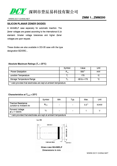
ZMM 1...ZMM200
Breakdown characteristics
Tj = constant (pulsed)
mA 10
MM5Z5V6T1G稳压二极管原厂DCY品牌推荐
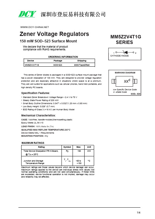
Zener Voltage Regulators150mW SOD–523Surface MountWe declare that the material of product compliance with RoHS requirements.ORDERING INFORMATIONDevice Package Shipping MM5ZXXXT1GSOD-5233000/Tape&ReelThis series of Zener diodes is packaged in a SOD–523surface mount package that has a power dissipation of 100mW.They are designed to provide voltage regulation protection and are especially attractive in situations where space is at a premium.They are well suited for applications such as cellular phones,hand held portables,and high density PC boards.Specification Features:•Standard Zener Breakdown Voltage Range –2.4V to 75V •Steady State Power Rating of 200mW•Small Body Outline Dimensions:0.047"x 0.032"(1.20mm x 0.80mm)•Low Body Height:0.028"(0.7mm)•ESD Rating of Class 3(>16kV)per Human Body ModelMechanical Characteristics:CASE:Void-free,transfer-molded,thermosetting plastic Epoxy Meets UL 94V-0LEAD FINISH:100%Matte Sn (Tin)QUALIFIED MAX REFLOW TEMPERATURE:260°C Device Meets MSL 1Requirements MOUNTING POSITION:AnyMAXIMUM RATINGSRatingSymbol Max Unit Total Device Dissipation FR−5Board,P D150mW@T A =25︒C Junction and Storage T J,Tstg−65to ︒CTemperature Range+150Maximum ratings are those values beyond which devicedamage can occur.Maximum ratings applied to the device are individual stress limit values (not normal operating conditions)and are not valid simultaneously.If these limits are exceeded,device functional operation is not implied,damage may occur and reliability may be affected.MM5Z2V4T1G SERIES12CATHODE ANODEMARKING DIAGRAMxx dxx=Specific Device Code d =Date CodeSOD–523MM5Z2V4T1G SERIES ELECTRICAL CHARACTERISTICS I(T A=25︒C unless otherwise noted,I FV F=0.9V Max.@I F=10mA for all types)Symbol ParameterVZ Reverse Zener Voltage@I ZT IZT Reverse Current VZVRVZ ZT Maximum Zener Impedance@I I R VFZT IZTIZK Reverse CurrentZZK Maximum Zener Impedance@I ZKIR Reverse Leakage Current@V RV R Reverse VoltageI F Forward Current Zener Voltage Regulator V F Forward Voltage@I FQV Z Maximum Temperature Coefficient of V ZC Max.Capacitance@V R=0and f=1MHz100(%)80DISS IP ATI ON 60 40POWER20255075100125150TEMPERATURE(︒C)Figure1.Steady State Power Derating MM5Z2V4T1G SERIESELECTRICAL CHARACTERISTICS (T A =25︒C unless otherwise noted,V F =0.9V Max.@I F =10mA for all types)Zener Voltage (Note 1)Zener Impedance Leakage CurrentQ V Z C ZZT(mV/k)@V =0V(Volts)@I@I ZT Z@II @VRZZKR@IZTf =1MHzDevice ZTZKRDevice Marking Min Nom Max mA W W mA m A Volts Min Max pF MM5Z2V4T1G 00 2.2 2.4 2.651001000 1.050 1.0−3.50450MM5Z2V7T1G 01 2.5 2.7 2.951001000 1.020 1.0−3.50450MM5Z3V0T1G 02 2.8 3.0 3.251001000 1.010 1.0−3.50450MM5Z3V3T1G 05 3.1 3.3 3.55951000 1.05 1.0−3.50450MM5Z3V6T1G 06 3.4 3.6 3.85901000 1.05 1.0−3.50450MM5Z3V9T1G 07 3.7 3.9 4.15901000 1.03 1.0−3.5−2.5450MM5Z4V3T1G 08 4.0 4.3 4.65901000 1.03 1.0−3.50450MM5Z4V7T1G 09 4.4 4.7 5.0580800 1.03 2.0−3.50.2260MM5Z5V1T1G 0A 4.8 5.1 5.4560500 1.02 2.0−2.7 1.2225MM5Z5V6T1G 0C 5.2 5.6 6.0540400 1.01 2.0−2.0 2.5200MM5Z6V2T1G 0E 5.8 6.2 6.6510100 1.03 4.00.4 3.7185MM5Z6V8T1G 0F 6.4 6.87.2515160 1.02 4.0 1.2 4.5155MM5Z7V5T1G 0G 7.07.57.9515160 1.01 5.0 2.5 5.3140MM5Z8V2T1G 0H 7.78.28.7515160 1.00.7 5.0 3.2 6.2135MM5Z9V1T1G 0K 8.59.19.6515160 1.00.27.0 3.87.0130MM5Z10VT1G 0L 9.41010.6520160 1.00.18.0 4.58.0130MM5Z11VT1G 0M 10.41111.6520160 1.00.18.0 5.49.0130MM5Z12VT1G 0N 11.41212.752580 1.00.18.0 6.010130MM5Z13VT1G 0P 12.413.2514.153080 1.00.18.07.011120MM5Z15VT1G 0T 14.31515.8530200 1.00.0510.59.213110MM5Z16VT1G 0U 15.316.217.1240200 1.00.0511.210.414105MM5Z18VT1G 0W 16.81819.1245225 1.00.0512.612.416100MM5Z20VT1G 0Z 18.82021.2255225 1.00.0514.014.41885MM5Z22VT1G 1020.82223.3255250 1.00.0515.416.42085MM5Z24VT1G 1122.824.225.6270120 1.00.0516.818.42280MM5Z27VT1G 1225.12728.9280300 1.00.0518.921.425.370MM5Z30VT1G 14283032280300 1.00.0521.024.429.470MM5Z33VT1G 18313335280300 1.00.0523.227.433.470MM5Z36VT1G 19343638290500 1.00.0525.230.437.470MM5Z39VT1G 203739412130500 1.00.0527.333.441.245MM5Z43VT1G 214043461150500 1.00.0530.137.646.640MM5Z47VT1G 1A 4447501170500 1.00.0532.942.051.840MM5Z51VT1G 1C 4851541180500 1.00.0535.746.657.240MM5Z56VT1G 1D 5256601200500 1.00.0539.252.263.840MM5Z62VT1G 1E 5862661215500 1.00.0543.458.871.635MM5Z68VT1G 1F 6468721240500 1.00.0547.665.679.835MM5Z75VT1G1G70757912555001.00.0552.573.488.6351.Zener voltage is measured with a pulse test current I Z at an ambient temperature of 25︒C.MM5Z2V4T1G SERIESSC-79/SOD-523DIMENSIONS (mm are the original dimensions)UNIT A b p c D E H E V m m0.70.350.2 1.30.9 1.70.150.50.250.11.10.71.5Note1.The marking bar indicates the cathode.OUTLINE REFERENCES EUROPEAN ISSUE DATEVERSION IECJEDECEIAJ PROJECTIONSOD523SC-7998-11-25。
DC4430(AO4430)场效应MOS管厂家DCY品牌推荐

TJ, Tstg RθJA
-55 to 150 75
oC oC/W
-1-
ELECTRICAL CHARACTERISTICS 一般电气特性
DC4430
Parameter 参数
符号
Test Condition 测试条件
最小值 典型值 最大值
单位
Static 静态参数
VDS = 24V, VGS = 0V
1
uA
Gate Body Leakage 漏极短路时截止栅电流
IGSS
VGS = ± 20V, VDS = 0V
± 100
nA
Forward Transconductance 正向跨导 Gate Resistance 栅极电阻
gfs
VDS = 5V, ID = 18A
ID
IDM
TA = 25oC PD
TA = 75oC
18 A
80
3 W
2.1
Operating Junction and Storage Temperature Range 使用及储存温度 Junction-to-Ambient Thermal Resistance (PCB mounted) 结环热阻
0.35
0.49
1.35
1.75
0.375 REF. 45°
1.27 TYP.
Maximum Ratings and Thermal Characteristics (TA = 25oC unless otherwise noted) 25 oC 极限参数和热特性
Parameter 极限参数
Symbol 符号
Turn-Off Fall Time 关断下降时间
ZMM100稳压二极管原厂DCY品牌推荐
ZMM 6V8
6.8
5
6.4...7.2
<8
<150
1
<0.1
<2
3
0.03...0.07
ZMM 7V5
7.5
5
7.0...7.9
<7
<50
1
<0.1
<2
5
0.03...0.07
ZMM 8V2
8.2
5
7.7...8.7
<7
<50
1
<0.1
<2
6.2
0.03...0.08
ZMM 9V1
9.1
5
8.5...9.6
These diodes are also available in DO-35 case with the type designation BZX55C...
ZMM 1...ZMM200
Absolute Maximum Ratings (Ta = 25oC)
Symbol
Value
Unit
Power Dissipation
K/W
3
10
7
ZMM...
5
r thA
4
3
2
0.5
102
7 0.2
5
4 0.1
3
0.05
2
0.02
0.01 10
7
V=0
5 4 3
2
1 10-5 10-4
tp
tp V= T
10-3
-2
10
T
10 -1 tp
PI
1
10 S
SM24 SOT-23TVS管原厂DCY品牌推荐

SM05 THRU SM36PROTECTION PRODUCTS TVS Diode ArrayDescriptionFeaturesCircuit Diagram Schematic & PIN ConfigurationThe SM series of transient voltage suppressors (TVS)are designed to protect components which areconnected to data and transmission lines from voltage surges caused by ESD (electrostatic discharge), EFT (electrical fast transients), and lightning .TVS diodes are characterized by their high surge capability, low operating and clamping voltages, and fast response time. This makes them ideal for use as board level protection of sensitive semiconductorcomponents. The dual-junction common-anode design allows the user to protect one bidirectional data line or two unidirectional lines. The low profile SOT23package allows flexibility in the design of crowded circuit boards.The SM series will meet the surge requirements of IEC 61000-4-2 (Formerly IEC 801-2), Level 4, Human Body Model for air and contact discharge.ApplicationsMechanical Characteristicsu Cellular Handsets and Accessories u Portable Electronics u Industrial Controls u Set-Top BoxuServers, Notebook, and Desktop PCu 300 watts peak pulse power (tp = 8/20µs)u Transient protection for data & power lines toIEC 61000-4-2 (ESD) 15kV (air), 8kV (contact)IEC 61000-4-4 (EFT) 40A (tp=5/50ns)IEC 61000-4-5 (Lightning) 12A (tp=1.2/50µs)u Protects one bidirectional line or two unidirectional linesu Working Voltages: 5V, 12V, 15V, 24 and 36V u Low clamping voltageu Solid-state silicon avalanche technologyu JEDEC SOT23 packageu Molding compound flammability rating: UL 94V-0u Marking : Marking Codeu Packaging : Tape and Reel per EIA 481Absolute Maximum RatingElectrical Characteristics50M S re t e m a r a P l o b m y S sn o i t i d n o C mu m i n i M la c i p y T mu m i x a M s t i n U e g a t l o V f f O -d n a t S e s r e v e R V M W R 5V e g a t l o V n w o d k a e r B e s r e v e R V R B I t A m 1=6V t n e r r u C e g a k a e L e s r e v e R I R V M W R C °52=T ,V 5=02A µeg a t l o V g n i p m a l C V C I P P ,A 1=s µ02/8=p t 8.9V t n e r r u C e s l u P k a e P m u m i x a M I p p s µ02/8=p t 71A e c n a t i c a p a C n o i t c n u J C j 2o t 1n i P V R z H M 1=f ,V 0=053F p ec n a t i c a p a C n o i t c n u J C jd n a 3o t 1n i P 3o t 2n i P V R zH M 1=f ,V 0=004Fp gn i t a R l o b m y S e u l a V s t i n U )s µ02/8=p t (r e w o P e s l u P k a e P P k p 003s t t a W t n e i b m A o t n o i t c n u J ,e c n a t s i s e R l a m r e h T q A J 655W /C °e r u t a r e p m e T g n i r e d l o S d a e L T L ).c e s 01(062C °e r u t a r e p m e T g n i t a r e p O T J 521+o t 55-C °er u t a r e p m e T e g a r o t S T GT S 051+o t 55-C°21M S re t e m a r a P l o b m y S sn o i t i d n o C mu m i n i M la c i p y T mu m i x a M s t i n U e g a t l o V f f O -d n a t S e s r e v e R V M W R 21V e g a t l o V n w o d k a e r B e s r e v e R V R B I t A m 1=3.31V t n e r r u C e g a k a e L e s r e v e R I R V M W R C°52=T ,V 21=1A µeg a t l o V g n i p m a l C V C I P P ,A 1=s µ02/8=p t 91V t n e r r u C e s l u P k a e P m u m i x a M I p p s µ02/8=p t 21A e c n a t i c a p a C n o i t c n u J C j 2o t 1n i P V R z H M 1=f ,V 0=021F p ec n a t i c a p a C n o i t c n u J C jd n a 3o t 1n i P 3o t 2n i P V R zH M 1=f ,V 0=051FpElectrical Characteristics (Continued)51M S re t e m a r a P l o b m y S s n o i t i d n o C m u m i n i M l a c i p y T mu m i x a M s t i n U e g a t l o V f f O -d n a t S e s r e v e R V M W R 51V e g a t l o V n w o d k a e r B e s r e v e R V R B I t A m 1=7.61Vt n e r r u C e g a k a e L e s r e v e R I R V M W R C °52=T ,V 51=1A µeg a t l o V g n i p m a l C V C I P P sµ02/8=p t ,A 1=42V t n e r r u C e s l u P k a e P m u m i x a M I p p s µ02/8=p t 01A e c n a t i c a p a C n o i t c n u J C j 2o t 1n i P V R z H M 1=f ,V 0=57F p e c n a t i c a p a C n o i t c n u J C j3o t 2d n a 3o t 1n i P V R zH M 1=f ,V 0=001Fp 42M S re t e m a r a P l o b m y S sn o i t i d n o C mu m i n i M l a c i p y T mu m i x a M s t i n U e g a t l o V f f O -d n a t S e s r e v e R V M W R 42V e g a t l o V n w o d k a e r B e s r e v e R V R B I t A m 1=7.62Vt n e r r u C e g a k a e L e s r e v e R I R V M W R C °52=T ,V 42=1A µeg a t l o V g n i p m a l C V C I P P sµ02/8=p t ,A 1=34V t n e r r u C e s l u P k a e P m u m i x a M I p p s µ02/8=p t 5A e c n a t i c a p a C n o i t c n u J C j 2o t 1n i P V R z H M 1=f ,V 0=05F p ec n a t i c a p a C n o i t c n u J C j3o t 2d n a 3o t 1n i P V R zH M 1=f ,V 0=06Fp 63M S re t e m a r a P l o b m y S s n o i t i d n o C m u m i n i M l a c i p y T mu m i x a M s t i n U e g a t l o V f f O -d n a t S e s r e v e R V M W R 63V e g a t l o V n w o d k a e r B e s r e v e R V R B I t A m 1=04Vt n e r r u C e g a k a e L e s r e v e R I R V M W R C °52=T ,V 63=1A µeg a t l o V g n i p m a l C V C I P P sµ02/8=p t ,A 1=06V t n e r r u C e s l u P k a e P m u m i x a M I p p s µ02/8=p t 4A e c n a t i c a p a C n o i t c n u J C j 2o t 1n i P V R z H M 1=f ,V 0=04F p ec n a t i c a p a C n o i t c n u J C j3o t 2d n a 3o t 1n i P V R zH M 1=f ,V 0=54FpTypical CharacteristicsNon-Repetitive Peak Pulse Power vs. Pulse Time1020304050607080901001100255075100125150Ambient Temperature - T A (oC)% o f R a t e d P o w e r o r I P PPower Derating CurvePulse Waveform0102030405060708090100110051015202530Time (µs)P e r c e n t o f I P Ple v e L t s r i F k a e P t n e r r u C )A (k a e P t n e r r u C s n 03t a )A (k a e P t n e r r u C s n 06t a )A (t s eT eg a t l o V tc a t n o C ()e g r a h c s i D )V k (ts e T e g a t l o V r i A ()e g r a h c s i D )V k (15.74822251844435.2221668436188510.010.11100.11101001000Pulse Duration - tp (µs)P e a k P u l s e P o w e r - P P P (k W )IEC 61000-4-2 Discharge ParametersESD Pulse Waveform (Per IEC 61000-4-2)Applications InformationDevice Schematic & Pin Configuration Device Connection OptionsThe SM series is designed to protect one bidirectionalor two unidirectional data or I/O lines operating at 5 to36 volts. Connection options are as follows:l Bidirectional: Pin 1 is connected to the data lineand pin 2 is connected to ground (Since the deviceis symmetrical, these connections may be re-versed). For best results, the ground connectionshould be made directly to a ground plane on theboard. The path length should be kept as short aspossible to minimize parasitic inductance. Pin 3 isnot connected.l Unidirectional: Data lines are connected to pin 1 and pin 2. Pin 3 is connected to ground. For best results, this pin should be connected directly to aground plane on the board. The path length should be kept as short as possible to minimize parasiticinductance.Circuit Board Layout Recommendations for Suppres-sion of ESD.Good circuit board layout is critical for the suppression of fast rise-time transients such as ESD. The following guidelines are recommended (Refer to application note SI99-01 for more detailed information):l Place the TVS near the input terminals or connec-tors to restrict transient coupling.l Minimize the path length between the TVS and the protected line.l Minimize all conductive loops including power and ground loops.l The ESD transient return path to ground should be kept as short as possible.l Never run critical signals near board edges.l Use ground planes whenever possible.RS-232 Transceiver ProtectionExampleOutline Drawing - SOT23Ordering Informationr e b m u N t r a P g n i k r o W e g a t l o V le e R r e p y t Q e z i S l e e R C T .50M S V 5000,3h c n I 7G T .50M S V 5000,01h c n I 31C T .21M S V 21000,3h c n I 7G T .21M S V 21000,01h c n I 31C T .51M S V 51000,3h c n I 7G T .51M S V 51000,01h c n I 31C T .42M S V 42000,3h c n I 7G T .42M S V 42000,01h c n I 31CT .63M S V63000,3hc n I 7Marking Codesre b m u N t r a P g n i k r a M e d o C 50M S 50M 21M S 21M 51M S 51M 42M S 42M 63M S 63M。
DC1234推荐LDO原厂DCY品牌
Output Voltage : 50mV increments A
e.g. ②=1,③=5,④=A 1.55V
Active 'High'
①
B
(no pull-down resistor built in)
Package Type
⑤
M
SOT-23-5L
C
Active 'Low' (pull-up resistor built in)
■ Features
Output Voltage Range: 0.85V to 1.8V (selectable in 50mV steps)
Highly Accurate : ±2%(less than 1.5V is ±30mV) Dropout Voltage : 300mV @ 100mA (1.5V type) High Ripple Rejection: 60dB (10kHz) Low Power Consumption: 50μA (TYP.) Maximum Output Current : 300mA(VIN≥2.5V) Standby Current : less than 0.1μA Internal protector: current limiter and short protector Small packages: SOT-23-5,SOT-353 and other
■ Applications
Mobile phones Cordless phones Modem Portable games
Portable AV equipment Reference voltage Battery powered equipment PCMCIA cards
稳压管z33 参数
稳压管z33 参数摘要:一、稳压管Z33的基本概念二、稳压管Z33的参数解析1.电压参数2.电流参数3.功率参数4.温度特性5.动态响应三、如何选择合适的稳压管Z33四、稳压管Z33的应用领域五、总结正文:一、稳压管Z33的基本概念稳压管Z33是一种常用的电子元件,主要用于电压稳压电路,确保输出电压在一定范围内保持稳定。
它具有广泛的应用,如电源模块、电子设备等。
稳压管Z33在我国的电子行业中有着广泛的应用,对其深入了解和掌握对于电子工程师来说至关重要。
二、稳压管Z33的参数解析1.电压参数:稳压管Z33的电压参数包括输入电压、输出电压和额定电压。
在选择稳压管时,应根据实际应用场景选择合适的电压参数,确保稳压管在工作过程中不会超过其额定电压。
2.电流参数:稳压管Z33的电流参数包括最大输入电流、最大输出电流和持续电流。
这些参数决定了稳压管的负载能力。
在选择稳压管时,应根据电路需求选择合适的电流参数,以确保稳压管能够满足电路的电流需求。
3.功率参数:稳压管Z33的功率参数表示其在工作过程中能够承受的最大功率。
在选择稳压管时,应结合电路的功耗需求,选择具有足够功率容量的稳压管。
4.温度特性:稳压管Z33的温度特性表示其在不同温度下的工作性能。
温度特性越好,稳压管的稳定性越高。
在选择稳压管时,应考虑实际应用场景的温度范围,选择具有合适温度特性的稳压管。
5.动态响应:稳压管Z33的动态响应表示其在负载变化时的电压调整速度。
动态响应越好,稳压管在负载变化时的输出电压稳定性越好。
在选择稳压管时,应根据电路对动态响应的需求,选择具有合适动态响应的稳压管。
三、如何选择合适的稳压管Z33在选择稳压管Z33时,应根据实际应用场景和电路需求,综合考虑电压、电流、功率、温度特性、动态响应等参数,选择性能合适的稳压管。
此外,还需关注稳压管的封装、尺寸、价格等因素,确保选型合理、经济。
四、稳压管Z33的应用领域稳压管Z33在我国的电子行业中有着广泛的应用,如电源模块、通信设备、电子仪器、家用电器等领域。
ZMM7V5稳压二极管原厂DCY品牌推荐
5
Ctot
4
3
2
VR=1V VR=2V
ZMM... Tj=25o C
100
7
VR=1V
5
VR=2V
4 3
2
10 1
2 3 4 5 10
2 3 4 5 100V Vz at Iz=5 mA
ZMM 1...ZMM200
Dynamic resistance versus Zener current
1000
5 4
r zj
3
2
ZMM... Tj=25o C
100
5 4 3
2
10
2.7
ZMM1
5
3.6
4
4.7
3
5.1
2
1
ZMM5.6
0.1 2
5
1
2
5 10 2
5 100mA
1
<0.1
<2
24
0.04...0.12
ZMM 36
36
5
34...38
<80
<220
1
<0.1
<2
27
0.04...0.12
ZMM 39
39
2.5
37...41
<90
<500
0.5
<0.1
<5
30
0.04...0.12
ZMM 43
43
2.5
40...46
<90
<500
0.5
<0.1
<5
33
0.04...0.12
SS34 SMC(DO-214AB)肖特基二极管原厂DCY品牌推荐
SS32 THRU SS36SURFACE MOUNT SCHOTTKY BARRIER RECTIFIERReverse Voltage -20 to 60 Volts Forward Current -3.0 AmperesFEATURES♦ Plastic package has Underwriters Laboratory Flammability Classification 94V-0♦ For surface mount applications ♦ Low profile package♦ Built-in strain relief, ideal for automated placement ♦ Easy pick and place ♦ Metal silicon junction, majority carrier conduction♦ Low power loss, high efficiency♦ High current capability, low forward voltage drop♦ For use in low voltage, high frequency inverters, free wheeling, and polarity protection applications ♦ High temperature soldering:250°C/10 seconds at terminalsMECHANICAL DATACase:JEDEC DO-214AB molded plastic bodyTerminals:Solder plated, solderable per MIL-STD-750,Method 2026Polarity:Color band denotes cathode end Weight:0.007 ounce 0.25 gramMAXIMUM RATINGS AND ELECTRICAL CHARACTERISTICSRatings at 25°C ambient temperature unless otherwise specified.SYMBOLS SS32SS33SS34SS35SS36UNITSDevice marking codeS2S3S4S5S6Maximum repetitive peak reverse voltage V RRM 2030405060Volts Maximum RMS voltage V RMS 1421283542Volts Maximum DC blocking voltageV DC 2030405060Volts Maximum average forward rectified current at T L (SEE FIG.1) (NOTE 2)I (AV) 3.0Amps Peak forward surge current8.3ms single half sine-wave superimposed on I FSM100.0Ampsrated load (JEDEC Method)Maximum instantaneous forward voltage at 3.0A(NOTE 1)V F 0.500.75Volts Maximum DC reverse current (NOTE 1)T A =25°C 0.5at rated DC blocking voltage T A =100°C I R 20.010.0mA Typical thermal resistance (NOTE 2)R ΘJA 55.0R ΘJL 17.0°C/WOperating junction temperature range T J -55 to +125-55 to +150°C Storage temperature rangeT STG-55 to +150°CNOTES:(1) Pulse test:300µs pulse width, 1% duty cycle(2) P .C.B.mounted 0.55 x 0.55”(14 x 14mm) copper pad areasDO-214ABDimensions in inches and (millimeters)。
MM5Z4V3T1G稳压二极管原厂DCY品牌推荐
Zener Voltage Regulators150mW SOD–523Surface MountWe declare that the material of product compliance with RoHS requirements.ORDERING INFORMATIONDevice Package Shipping MM5ZXXXT1GSOD-5233000/Tape&ReelThis series of Zener diodes is packaged in a SOD–523surface mount package that has a power dissipation of 100mW.They are designed to provide voltage regulation protection and are especially attractive in situations where space is at a premium.They are well suited for applications such as cellular phones,hand held portables,and high density PC boards.Specification Features:•Standard Zener Breakdown Voltage Range –2.4V to 75V •Steady State Power Rating of 200mW•Small Body Outline Dimensions:0.047"x 0.032"(1.20mm x 0.80mm)•Low Body Height:0.028"(0.7mm)•ESD Rating of Class 3(>16kV)per Human Body ModelMechanical Characteristics:CASE:Void-free,transfer-molded,thermosetting plastic Epoxy Meets UL 94V-0LEAD FINISH:100%Matte Sn (Tin)QUALIFIED MAX REFLOW TEMPERATURE:260°C Device Meets MSL 1Requirements MOUNTING POSITION:AnyMAXIMUM RATINGSRatingSymbol Max Unit Total Device Dissipation FR−5Board,P D150mW@T A =25︒C Junction and Storage T J,Tstg−65to ︒CTemperature Range+150Maximum ratings are those values beyond which devicedamage can occur.Maximum ratings applied to the device are individual stress limit values (not normal operating conditions)and are not valid simultaneously.If these limits are exceeded,device functional operation is not implied,damage may occur and reliability may be affected.MM5Z2V4T1G SERIES12CATHODE ANODEMARKING DIAGRAMxx dxx=Specific Device Code d =Date CodeSOD–523MM5Z2V4T1G SERIES ELECTRICAL CHARACTERISTICS I(T A=25︒C unless otherwise noted,I FV F=0.9V Max.@I F=10mA for all types)Symbol ParameterVZ Reverse Zener Voltage@I ZT IZT Reverse Current VZVRVZ ZT Maximum Zener Impedance@I I R VFZT IZTIZK Reverse CurrentZZK Maximum Zener Impedance@I ZKIR Reverse Leakage Current@V RV R Reverse VoltageI F Forward Current Zener Voltage Regulator V F Forward Voltage@I FQV Z Maximum Temperature Coefficient of V ZC Max.Capacitance@V R=0and f=1MHz100(%)80DISS IP ATI ON 60 40POWER20255075100125150TEMPERATURE(︒C)Figure1.Steady State Power Derating MM5Z2V4T1G SERIESELECTRICAL CHARACTERISTICS (T A =25︒C unless otherwise noted,V F =0.9V Max.@I F =10mA for all types)Zener Voltage (Note 1)Zener Impedance Leakage CurrentQ V Z C ZZT(mV/k)@V =0V(Volts)@I@I ZT Z@II @VRZZKR@IZTf =1MHzDevice ZTZKRDevice Marking Min Nom Max mA W W mA m A Volts Min Max pF MM5Z2V4T1G 00 2.2 2.4 2.651001000 1.050 1.0−3.50450MM5Z2V7T1G 01 2.5 2.7 2.951001000 1.020 1.0−3.50450MM5Z3V0T1G 02 2.8 3.0 3.251001000 1.010 1.0−3.50450MM5Z3V3T1G 05 3.1 3.3 3.55951000 1.05 1.0−3.50450MM5Z3V6T1G 06 3.4 3.6 3.85901000 1.05 1.0−3.50450MM5Z3V9T1G 07 3.7 3.9 4.15901000 1.03 1.0−3.5−2.5450MM5Z4V3T1G 08 4.0 4.3 4.65901000 1.03 1.0−3.50450MM5Z4V7T1G 09 4.4 4.7 5.0580800 1.03 2.0−3.50.2260MM5Z5V1T1G 0A 4.8 5.1 5.4560500 1.02 2.0−2.7 1.2225MM5Z5V6T1G 0C 5.2 5.6 6.0540400 1.01 2.0−2.0 2.5200MM5Z6V2T1G 0E 5.8 6.2 6.6510100 1.03 4.00.4 3.7185MM5Z6V8T1G 0F 6.4 6.87.2515160 1.02 4.0 1.2 4.5155MM5Z7V5T1G 0G 7.07.57.9515160 1.01 5.0 2.5 5.3140MM5Z8V2T1G 0H 7.78.28.7515160 1.00.7 5.0 3.2 6.2135MM5Z9V1T1G 0K 8.59.19.6515160 1.00.27.0 3.87.0130MM5Z10VT1G 0L 9.41010.6520160 1.00.18.0 4.58.0130MM5Z11VT1G 0M 10.41111.6520160 1.00.18.0 5.49.0130MM5Z12VT1G 0N 11.41212.752580 1.00.18.0 6.010130MM5Z13VT1G 0P 12.413.2514.153080 1.00.18.07.011120MM5Z15VT1G 0T 14.31515.8530200 1.00.0510.59.213110MM5Z16VT1G 0U 15.316.217.1240200 1.00.0511.210.414105MM5Z18VT1G 0W 16.81819.1245225 1.00.0512.612.416100MM5Z20VT1G 0Z 18.82021.2255225 1.00.0514.014.41885MM5Z22VT1G 1020.82223.3255250 1.00.0515.416.42085MM5Z24VT1G 1122.824.225.6270120 1.00.0516.818.42280MM5Z27VT1G 1225.12728.9280300 1.00.0518.921.425.370MM5Z30VT1G 14283032280300 1.00.0521.024.429.470MM5Z33VT1G 18313335280300 1.00.0523.227.433.470MM5Z36VT1G 19343638290500 1.00.0525.230.437.470MM5Z39VT1G 203739412130500 1.00.0527.333.441.245MM5Z43VT1G 214043461150500 1.00.0530.137.646.640MM5Z47VT1G 1A 4447501170500 1.00.0532.942.051.840MM5Z51VT1G 1C 4851541180500 1.00.0535.746.657.240MM5Z56VT1G 1D 5256601200500 1.00.0539.252.263.840MM5Z62VT1G 1E 5862661215500 1.00.0543.458.871.635MM5Z68VT1G 1F 6468721240500 1.00.0547.665.679.835MM5Z75VT1G1G70757912555001.00.0552.573.488.6351.Zener voltage is measured with a pulse test current I Z at an ambient temperature of 25︒C.MM5Z2V4T1G SERIESSC-79/SOD-523DIMENSIONS (mm are the original dimensions)UNIT A b p c D E H E V m m0.70.350.2 1.30.9 1.70.150.50.250.11.10.71.5Note1.The marking bar indicates the cathode.OUTLINE REFERENCES EUROPEAN ISSUE DATEVERSION IECJEDECEIAJ PROJECTIONSOD523SC-7998-11-25。
- 1、下载文档前请自行甄别文档内容的完整性,平台不提供额外的编辑、内容补充、找答案等附加服务。
- 2、"仅部分预览"的文档,不可在线预览部分如存在完整性等问题,可反馈申请退款(可完整预览的文档不适用该条件!)。
- 3、如文档侵犯您的权益,请联系客服反馈,我们会尽快为您处理(人工客服工作时间:9:00-18:30)。
ZMM 150
150
1
138...156
<1250 <6500
0.1
<0.1
<10
110
0.05...0.12
ZMM 160
160
1
153...171
<1400 <7000
0.1
<0.1
<10
120
0.05...0.12
ZMM 180
180
1
168...191
<1700 <8500
0.1
<0.1
<10
130
0.05...0.12
ZMM 200
200
1
188...212 <2000 <10000 0.1
<0.1
<10
150
0.05...0.12
1) Tested with pulses tp = 20 ms. 2) Valid provided that electrodes are kept at ambient temperature
<85
<600
1
<2
<40
1
-0.08...-0.05
ZMM 3V9
3.9
5
3.7...4.1
<85
<600
1
<2
<40
1
-0.08...-0.05
ZMM 4V3
4.3
5
4.0...4.6
<75
<600
1
<1
<20
1
-0.06...-0.03
ZMM 4V7
4.7
5
4.4...5.0
<60
<600
1
<0.5
Reverse Leakage Current
Ta =25oC Ta = 125oC
μA
μA
IR at VR V
Temp coefficient of Zener Voltage
TKvz %/K
ZMM 13)
0.75
5
0.7...0.8
<8
<50
1
--
--
--
-0.26...-0.23
ZMM 2V0
mW
ZMM...
500
P tot
400
300
200
100
0 0
100 Tamb
200o C
Pulse thermal resistance versus pulse duration
Valid provided that the electrodes are kept at ambient temperature.
<2
9.1
0.03...0.11
ZMM 13
13
5
12.4...14.1
<26
<110
1
<0.1
<2
10
0.03...0.11
ZMM 15
15
5
13.8...15.6
<30
<110
1
<0.1
<2
11
0.03...0.11
ZMM 16
16
5
15.3...17.1
<40
<170
1
<0.1
<2
12
0.03...0.11
ZMM 18 ZMM 22 ZMM 27
ZMM... Tj=25o C
ZMM 33 ZMM 36
0
0
10
20
30
40 V
Vz
ZMM 1...ZMM200
Breakdown characteristics
Tj = constant (pulsed)
mA 10
Iz 8
These diodes are also available in DO-35 case with the type designation BZX55C...
ZMM 1...ZMM200
Absolute Maximum Ratings (Ta = 25oC)
Symbol
Value
Unit
Power Dissipation
6
ZMM 39
Test current Iz 5mA
ZMM 43
ZMM 51 ZMM 47
ZMM... Tj=25o C
4
2
0
0
Hale Waihona Puke 102030
40
50
60
70
80
90
100 V
Vz
Forward characteristics
mA
3
10
10 2 iF
10
1
10 -1
-2
10 10-3
10-4 10-5
5 4
r zj
3
2
ZMM... Tj=25o C
100
5 4 3
2
10
2.7
ZMM1
5
3.6
4
4.7
3
5.1
2
1
ZMM5.6
0.1 2
5
1
2
5 10 2
5 100mA
5
Ctot
4
3
2
VR=1V VR=2V
ZMM... Tj=25o C
100
7
VR=1V
5
VR=2V
4 3
2
10 1
2 3 4 5 10
2 3 4 5 100V Vz at Iz=5 mA
ZMM 1...ZMM200
Dynamic resistance versus Zener current
1000
0
ZMM...
Tj=100 oC Tj=25 oC
0.2
0.4
0.6
0.8
1V
VF
Admissible power dissipation versus ambient temperature
Valid provided that electrodes are kept at ambient temperature.
2.7
5
2.5...2.9
<85
<600
1
<10
<50
1
-0.09...-0.06
ZMM 3V0
3.0
5
2.8...3.2
<85
<600
1
<4
<40
1
-0.08...-0.05
ZMM 3V3
3.3
5
3.1...3.5
<85
<600
1
<2
<40
1
-0.08...-0.05
ZMM 3V6
3.6
5
3.4...3.8
K/W
3
10
7
ZMM...
5
r thA
4
3
2
0.5
102
7 0.2
5
4 0.1
3
0.05
2
0.02
0.01 10
7
V=0
5 4 3
2
1 10-5 10-4
tp
tp V= T
10-3
-2
10
T
10 -1 tp
PI
1
10 S
Capacitance versus Zener voltage
pF 1000
7
<10
1
-0.05...+0.02
ZMM 5V1
5.1
5
4.8...5.4
<35
<550
1
<0.1
<2
1
-0.02...+0.02
ZMM 5V6
5.6
5
5.2...6.0
<25
<450
1
<0.1
<2
1
-0.05...+0.05
ZMM 6V2
6.2
5
5.8...6.6
<10
<200
1
<0.1
<2
2
0.03...0.06
ZMM 6V8
6.8
5
6.4...7.2
<8
<150
1
<0.1
<2
3
0.03...0.07
ZMM 7V5
7.5
5
7.0...7.9
<7
<50
1
<0.1
<2
5
0.03...0.07
ZMM 8V2
8.2
5
7.7...8.7
<7
<50
1
<0.1
<2
6.2
0.03...0.08
ZMM 9V1
9.1
5
8.5...9.6
ZMM 47
47
2.5
44...50
<110
<600
0.5
<0.1
<5
36