接触热阻
接触热阻定义
接触热阻定义什么是接触热阻?接触热阻本身是一个相对比较简单的理论,但是对于物理学和热力学来说,它却是一个极为重要的概念。
接触热阻是指两种物体表面接触时表面之间的热阻力,与传播热量有关。
热阻是热传导性的一个参数,而接触热阻则是在两个表面之间存在的热阻力。
当两个物体的温度不同,它们之间的热流动就会发生。
如果这两个物体表面完全是接触的,那么它们之间的热量流动速度可能就会受到一些约束。
这种约束称作接触热阻,包括气体-气体、气体-液体、气体-固体、液体-液体、液体-固体以及固体-固体等等多种不同的热阻类型。
我们可以用一个简单的例子来说明接触热阻的概念:如果在做饭的时候,我们使用一把凉铁勺去搅动热汤,那么由于热汤和铁勺之间的接触热阻,铁勺会比汤稍微冷一些。
同样的,如果我们使用一个热的勺子去搅匀一杯冷饮,那么这个勺子也会变得稍微凉一些。
这种热量的传播,它就是取决于两个表面的接触热阻的。
如何计算接触热阻?计算接触热阻的方法取决于热传递的方式。
根据不同的热传递方式,计算接触热阻的基本公式也不同。
在气体-气体之间的热传递中,接触热阻的计算方法主要使用代表气体流动的能量公式。
在液体-气体和液体-液体之间的热传递中,接触热阻的计算方法则会使用液流动的能量公式。
在这些情况下,计算接触热阻需要对不同物质的能量方程进行求解。
而在不同的热传递中,接触热阻的计算方式也不一样。
在气体-固体热传递中,接触热阻的计算方式主要使用冷却效果进行求解。
在液体-固体热传递中,接触热阻的计算方法则需要用到液流动的基本方程。
最后,对于固体-固体之间的热传递,可以通过经验公式进行计算。
这个经验公式是将接触热阻与材料的热导率、表面的平整程度和压力等参数联系在一起进行计算的。
综合考虑接触面的粗糙度、表面磨损和材料导热性能等影响,可以得到更加准确的结果。
优化接触热阻的方法接触热阻是影响热传递效率的一个重要因素。
在很多工业过程中,我们需要用到高效的热传递技术。
接触式热电阻
接触式热电阻接触式热电阻是一种温度传感器,其原理是基于导体或半导体的电阻值随温度变化的特性。
接触式热电阻通过与被测物体接触来感知温度,并将温度转换为电阻值的变化,然后通过测量电阻值的变化来测量温度。
接触式热电阻具有测量精度高、稳定性好、响应速度快、耐腐蚀等特点,被广泛应用于工业自动化、能源、化工、机械、冶金等领域。
常见的接触式热电阻有铜热电阻、镍热电阻和铂热电阻等。
不同类型的热电阻具有不同的测温范围和精度,需要根据实际需求进行选择。
在使用接触式热电阻时,需要注意以下几点:1. 正确安装热电阻,保证与被测物体紧密接触,避免产生测量误差;2. 避免在高温或腐蚀性介质中使用热电阻,以免损坏传感器;3. 定期检查和校准热电阻,确保测温准确性和稳定性。
接触式热电阻的测量电路通常采用电桥电路,通过测量电桥的输出电压或电阻值来计算温度。
常见的电桥电路有铜热电阻电桥、镍热电阻电桥和铂热电阻电桥等。
在测量电路中,需要根据不同类型的热电阻选择相应的电桥电路,同时需要选择合适的电源电压和信号输出方式。
在选择电源电压时,需要考虑热电阻的阻值和所需的测量精度。
在选择信号输出方式时,需要考虑系统的接口需求和信号处理能力。
此外,为了提高测量的准确性和稳定性,可以采用温度补偿、信号滤波和数字信号处理等技术。
温度补偿技术可以通过测量环境温度来修正热电阻的阻值变化,提高测温准确性;信号滤波技术可以通过滤波电路来消除噪声干扰,提高信号稳定性;数字信号处理技术可以通过算法处理来进一步提高测温精度和稳定性。
总之,接触式热电阻作为一种重要的温度传感器,在工业自动化、能源、化工等领域得到广泛应用。
通过选择合适的测量电路和技术,可以实现高精度、高稳定性和快速响应的测温系统,为工业生产和科学实验提供重要的技术支持。
接触热阻 导热系数

"接触热阻" 和"导热系数" 都是与热传导相关的概念,它们在热学和工程领域中具有重要意义。
1. **接触热阻**(Thermal Contact Resistance):接触热阻是指在两个材料或物体的接触界面上,由于不完美的接触而导致的热阻。
当两个物体接触时,其表面之间通常存在微小的间隙或不均匀性,这会导致热量传导的障碍。
接触热阻通常以温度差、接触面积和材料性质等因素来描述,它的值通常以温度差除以接触界面上的热流率来表示。
2. **导热系数**(Thermal Conductivity):导热系数是一个材料的热传导性能的度量。
它表示了材料在单位时间内从高温区传导热量到低温区的能力。
导热系数通常以热流密度、材料厚度和温度差来计算。
不同材料具有不同的导热系数,例如,金属通常具有高导热系数,而绝缘材料具有较低的导热系数。
icepak接触热阻设置

icepak接触热阻设置摘要:I.引言- 介绍icepak 接触热阻的概念II.接触热阻的设置- 接触热阻的作用- 如何设置接触热阻1.选择热阻类型2.设置热阻参数3.调整热阻位置III.接触热阻设置的影响- 影响热阻的性能- 影响系统的散热效果IV.总结- 概括接触热阻设置的重要性- 提出建议和展望正文:I.引言icepak 是一款广泛应用于电子产品散热设计的软件,能够模拟电子设备在工作过程中的热传递现象。
接触热阻是影响热传递效果的一个重要参数,合理的接触热阻设置能够有效提高系统的散热性能。
II.接触热阻的设置接触热阻主要是指在接触的物体之间产生的热阻,它影响了热量在接触物体之间的传递。
在icepak 中,接触热阻可以通过以下步骤进行设置:1.选择热阻类型:icepak 提供了多种热阻类型供用户选择,如恒定热阻、线性热阻、指数热阻等。
用户需要根据实际需求选择合适的热阻类型。
2.设置热阻参数:用户需要为热阻设置合适的参数,如热阻值、热导率等。
这些参数将直接影响热阻的效果。
3.调整热阻位置:在icepak 中,用户可以自由调整热阻的位置,以达到最佳的热阻效果。
III.接触热阻设置的影响接触热阻设置的合理与否,将直接影响热阻的性能以及整个系统的散热效果。
如果接触热阻设置不合理,可能导致系统散热不畅,进而影响设备的稳定性和使用寿命。
IV.总结总的来说,接触热阻设置在icepak 软件中是一个十分重要的环节。
合理的接触热阻设置能够有效提高系统的散热性能,从而保证设备的稳定运行。
icepak接触热阻
Icepak接触热阻简介Icepak接触热阻是一个用于热分析和热设计的计算机软件。
它可以模拟和优化电子设备中的热传导和热辐射问题。
本文将详细介绍Icepak接触热阻的原理、应用和优势。
原理Icepak接触热阻基于有限元法和计算流体力学(CFD)技术,通过求解热传导方程和Navier-Stokes方程来模拟和分析热传导和热辐射问题。
它可以考虑不同材料的热导率、热容和密度,并且可以模拟不同的边界条件和热源。
应用Icepak接触热阻广泛应用于电子设备的热管理和设计中。
以下是一些常见的应用场景:1. 散热器设计Icepak接触热阻可以帮助工程师设计散热器,以提高电子设备的散热效果。
它可以模拟散热器的热传导和对流散热,并优化散热器的结构和材料,以提高散热效率。
2. 硅芯片热管理在集成电路中,硅芯片的热管理是非常重要的。
Icepak接触热阻可以模拟硅芯片的热传导和辐射散热,并通过优化散热结构和材料,提高硅芯片的散热性能,保证芯片的正常工作。
3. 电池热管理电动汽车、移动设备等电池的热管理是一个关键问题。
Icepak接触热阻可以模拟电池的热传导和对流散热,帮助设计师优化电池的散热结构和材料,延长电池的使用寿命并提高安全性。
4. LED灯散热LED灯作为一种新型的照明设备,热管理也是一个重要问题。
Icepak接触热阻可以模拟LED灯的热传导和辐射散热,并优化LED灯的结构和材料,提高灯的散热效果,延长灯的使用寿命。
优势Icepak接触热阻相比传统的热分析方法具有以下优势:1. 高精度Icepak接触热阻使用有限元法和CFD技术,可以精确地模拟和分析热传导和热辐射问题,提供高精度的热分析结果。
2. 快速计算Icepak接触热阻采用并行计算和优化算法,可以快速计算大规模的热传导和热辐射问题,提高工程师的工作效率。
3. 可视化分析Icepak接触热阻提供丰富的可视化分析工具,可以直观地展示热传导和热辐射问题的分布和变化趋势,帮助工程师理解和优化热管理方案。
接触表面的压力接触热阻
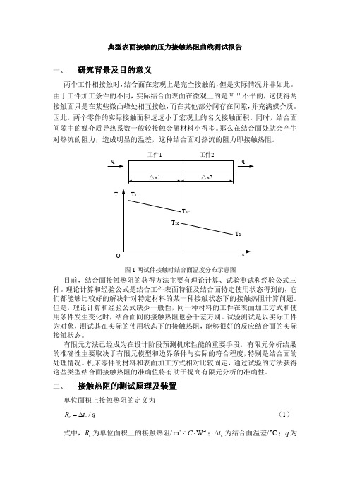
典型表面接触的压力接触热阻曲线测试报告一、 研究背景及目的意义两个工件相接触时,结合面在宏观上是完全接触的,但是实际情况并非如此。
由于工件加工条件的不同,实际结合面表面在微观上的是凹凸不平的,这使得两接触面只是在某些微凸峰处相互接触,而在其他部分间存在间隙,并充满媒介质。
因此,两个零件的实际接触面积远远小于宏观上的名义接触面积。
同时,结合面间隙中的媒介质导热系数一般较接触金属材料小得多。
那么在结合面处就会产生对热流的阻力,造成明显的温差,这种结合面对热流的阻力即接触热阻。
工件1工件2图1两试件接触时结合面温度分布示意图 目前,结合面接触热阻的获得方法主要有理论计算、试验测试和经验公式三种。
理论计算和经验公式是结合工件表面特征及结合面特定使用状态得到的,它们都能够比较好的解决针对特定材料的某一种接触状态下的接触热阻计算问题。
但是,理论计算和经验公式缺少一般性,同一种材料的工件在表面加工方式和使用条件发生变化时,结合面间的接触热阻也会千差万别。
试验测试是以实际工件为对象,测试其在实际的使用状态下的接触热阻,能够很好的反应结合面的实际接触状态。
有限元方法已经成为在设计阶段预测机床性能的重要手段,有限元分析结果的准确性主要取决于有限元模型和边界条件与实际的符合程度,特别是结合面的处理情况。
机床零件的材料和表面加工方式相对比较固定,通过试验的方法获得这些类型结合面接触热阻的准确值将有助于提高有限元分析的准确性。
二、 接触热阻的测试原理及装置单位面积上接触热阻的定义为/c c R t q =∆ (1) 式中,c R 为单位面积上的接触热阻/2-1m W C ⋅⋅;c t ∆为结合面温差/°C ;q 为单位面积上的热流量/-2W m ⋅。
接触热导的定义为1/c c h R = (2) 式中,c h 为结合面的接触热导/-2o -1W m C ⋅⋅。
由式子(1)中单位面积接触热阻的定义可以看到,接触热阻主要取决于结合面的温降c t ∆和通过结合面单位面积上的热量q 。
接触热阻的定义

接触热阻的定义
嘿,咱说说接触热阻是啥。
有一回冬天,我坐在一个金属椅子上,哎呀,那叫一个凉啊。
我就想,这金属椅子和我的屁股之间好像有个东西在阻碍热量传递呢。
这就有点像接触热阻。
接触热阻呢,就是两个物体接触的时候,阻碍热量从一个物体传到另一个物体的那个东西。
比如说,你把热水杯放在桌子上,杯子和桌子接触的地方,热量不是一下子就全传过去了,有一部分就被挡住了,这就是接触热阻在起作用。
我记得有一次我去修电脑,那个师傅说电脑的芯片和散热器之间如果接触不好,就会有很大的接触热阻,这样芯片就容易过热。
所以啊,接触热阻就是这么个捣乱的家伙,不让热量好好地传递。
下次你感觉到两个东西接触的时候热量传递不顺畅,说不定就是接触热阻在作怪呢。
焊料接触热阻-概述说明以及解释

焊料接触热阻-概述说明以及解释1.引言1.1 概述概述部分的内容可以包括对焊料接触热阻的基本概念和作用进行简要介绍。
焊料接触热阻是指在焊接过程中,焊料与焊接材料或其他接触物之间存在的热阻。
焊料接触热阻的大小直接影响着焊接过程中的热传导效率和焊接接头的质量。
焊料是一种用于连接金属件或其他材料的材料。
它通过熔化并与被连接材料接触,形成一层液态或固态的连接层,将被连接材料牢固地连接在一起。
焊料的种类繁多,包括焊丝、焊条、焊剂等,可以根据被连接材料的不同选择不同类型的焊料。
焊料接触热阻在焊接过程中起到了重要的作用。
首先,焊料接触热阻能够影响焊接过程中的热传导效率。
热传导是焊接过程中热能传递的重要方式,它直接影响着焊缝的形成和焊接接头的质量。
如果焊料接触热阻过高,热能传递效率会降低,导致焊缝不充分或产生焊接缺陷。
其次,焊料接触热阻还会影响焊接接头的温度分布。
如果焊料接触热阻不均匀,热量分布也会不均匀,导致焊接接头出现温度应力、变形甚至断裂等问题。
因此,了解和研究焊料接触热阻的意义重大。
通过控制焊料接触热阻,可以提高焊接过程中的热传导效率,改善焊接接头的质量,进而提高焊接接头的强度和可靠性。
同时,深入研究焊料接触热阻的影响因素,可以为焊接工艺的优化和提升提供理论指导和技术支持。
综上所述,焊料接触热阻作为一项重要的焊接参数,对焊接过程和焊接接头的质量有着直接的影响。
因此,理解和掌握焊料接触热阻的相关知识是进行高质量焊接的关键之一。
在接下来的文章中,我们将详细介绍焊料接触热阻的影响因素和研究方向,以期为焊接技术的发展和应用提供有益的指导。
1.2文章结构文章结构部分的内容:文章结构部分旨在介绍本文的组织方式和章节安排,以帮助读者更好地理解文章的内容和逻辑结构。
本文分为引言、正文和结论三个部分。
在引言部分,我们将首先概述焊料接触热阻的背景和意义,介绍本文的目的和重要性。
接下来是正文部分,将重点介绍焊料的基本概念和作用,以及焊料接触热阻的意义和影响因素。
- 1、下载文档前请自行甄别文档内容的完整性,平台不提供额外的编辑、内容补充、找答案等附加服务。
- 2、"仅部分预览"的文档,不可在线预览部分如存在完整性等问题,可反馈申请退款(可完整预览的文档不适用该条件!)。
- 3、如文档侵犯您的权益,请联系客服反馈,我们会尽快为您处理(人工客服工作时间:9:00-18:30)。
—We analyze fundamental issues related to the thermal and electrical stability of a coated conductor during its operation. We address the role of conductive buffer layers in the stability of Ni-based coated conductors, and the effect of a metallic cap layer on the electrical properties of Ni alloy-based superconducting tapes. For the first case we report on the fabrication of a fully conductive RABiTS architecture formed of bilayers of conductive oxides SrRuO3 and LaNiO3 on textured Ni tapes. For the second case we discuss measurements of current-voltage relations on Ag/YBa2Cu3O7-δ and Cu/Ag/ YBa2Cu3O7-δprototype multilayers on insulating substrates. Limitations on the overall tape structure and properties that are posed by the stability requirement are presented.Index Terms—Buffer layers, contact resistance, critical currents, metallic oxides, superconducting tapes.I. I NTRODUCTIONt the stage of implementation, coated conductor tapeswill have to be electrically and thermally stabilizedagainst transient conditions in which the current may exceed I c of the HTS coating. Coated conductors are typically formed of a 50 µm thick metallic substrate (Ni or Ni-alloys), Manuscript received September 17, 2000. The submitted manuscript has been authored by a contractor of the U.S. Government under contract DE-AC05-00OR22725. Accordingly, the U.S. Government retains a nonexclusive, royalty-free license to publish or reproduce the published formof this contribution, or allow others to do so, for U.S. Government purposes.C. Cantoni is with Solid State Division, Oak Ridge National Laboratory, Oak Ridge, TN 37831-6061 USA (telephone: 865-574-6264, e-mail: cantonic@).T. Aytug is with Solid State Division, Oak Ridge National Laboratory, Oak Ridge, TN 37831-6061 USA (telephone: 865-574-6271, e-mail: aytug@).D. T. Verebelyi was with Solid State Division, Oak Ridge National Laboratory, Oak Ridge, TN 37831-6061. He is now with American Superconductor Corporation (telephone: 508-621-4368, e-mail: dverebelyi@).M. Paranthaman is with Chemical and Analytical Sciences Division, Oak Ridge National Laboratory, Oak Ridge, TN 37831-6100 (telephone: 865-574-5045, e-mail: paranthamanm@).E. D. Specht is with Metals and Ceramics Division, Oak Ridge National Laboratory, Oak Ridge, TN 37831-6118 (telephone: 865-574-7682, e-mail: spechted@).D. P. Norton was with Solid State Division, Oak Ridge National Laboratory, Oak Ridge, TN 37831-6059. He is now with Department of Materials Science and Engineering, University of Florida, Gainesville, FL 32611-6400 (telephone: 352-846-0525, e-mail: dnort@).D. K. Christen is with Solid State Division, Oak Ridge National Laboratory, Oak Ridge, TN 37831-6061 USA (telephone: 865-574-6269,e-mail: christendk@). one or more insulating oxide buffer layers with a total thickness of 0.5-1 µm, and an HTS film thicker than 1µm. Asa benchmark we can assume that the HTS film (usually YBCO) carries a current density of 1×10⁶ A/cm2 in the superconducting state at liquid nitrogen temperatures (64 - 77 K) and in self magnetic field. In the event of a transient to the dissipative regime, the power generated per unit area in suchan electrically-isolated 2 µm thick HTS layer would exceed 104 W/cm2, resulting in destruction of the superconductor.In order to remove the heat generated from the HTS layer, and restore superconductivity, the superconducting film has tobe electrically coupled to a conductive metallic layer. This coupling provides a lower overall resistivity during transient losses of superconductivity, and, consequently, a lower dissipation in the net conductor. In addition, coupling to a good metal greatly increases the thermal conductivity of the entire tape, significantly improving the outflow of heat to the surrounding refrigerant bath, and, therefore, the cooling rateof the conductor. The efficiency of cooling depends on many parameters of the application design. However, we consider the simple case of steady-state heat flow removed by contactof the tape with boiling liquid nitrogen. Then, the maximum temperature excursion is determined by limiting the heat fluxto a value below the critical heat flux of LN2 at 77 K (10- 20 W/cm2) [1].Electrical coupling of the superconducting film to the metal layer can be envisioned in two different ways. The textured metal substrate of sufficiently low resistivity, as in the case of pure Ni or Cu, can itself provide the necessary stability for the HTS film if the buffer layer is conducting rather than insulating. For a 2 µm thick YBCO coating that is electrically connected to an underlying 50 µm thick base metal tape of pure nickel, the normal-state heat flux from each unit surface area would be only about 4 W/cm2 per tape surface, well below the critical heat flux of liquid nitrogen.On the other hand, a conductive buffer layer is not an effective route if the substrate of choice is a Ni alloy, which typically would have a resistivity comparable to the normal state resistivity of the superconductor (~100 µΩ-cm @ 100 K). In this case, stability can be achieved by applying a metal overlayer such as Cu or Ag on the superconducting film.Figure 1 shows the calculated dependence on the substrate resistivity of the metal-layer thickness necessary to maintain the transient heat flux below 5 W/cm2when an HTS film 2 µm thick, carrying a current density of 1 MA/cm2, is drivento the dissipative state. The effect on the overall tape currentConductive Buffer Layers and Overlayers forthe Thermal Stability of Coated ConductorsC. Cantoni, T. Aytug,D. T. Verebelyi, M. Paranthaman,E. D. Specht, D. P. Norton, andD. K. ChristenAFig.1. The approximate calculated thickness required of a highly conductivecap layer (Cu or Ag), in order to stabilize the transient dissipative heat flux to a value ~5 W/cm 2 (2.5 W/cm 2 per tape surface), as a function of the 50 µm thick substrate-tape resistivity. The HTS layer is taken to be 2 µm thick, carrying a current density of 1 MA/cm 2. The contact resistancebetween the HTS and the metal layer is assumed to be negligible. The insetshows the same plot expanded in the region of low resistivities.density, J E , is also shown. In this paper we discuss important aspects of both approaches. We report on the development ofa conductive bilayer composed of LaNiO 3 and SrRuO 3 for Ni-based coated conductors. In addition, we address some stability issues for alloy-based coated conductors by testing transport properties of structures formed by a metal cap layer deposited on YBCO films on single crystal SrTiO 3 (STO) substrates.II. EXPERIMENTALBoth SrRuO 3 (SRO) and LaNiO 3 (LNO) are perovskite-type, conductive metallic oxides with pseudocubic lattice parameters of 3.96 Å and 3.86 Å, and room temperature resistivities of about 300 µΩ-cm and 600 µΩ-cm, respectively. We have previously shown that highly textured LNO buffer layers can be successfully deposited onto Ni tapes [2] and we have subsequently optimized the deposition conditions to reproduce in these films the same degree of in-plane and out-of-plane texture of the Ni substrate [3]. The LNO films for this study were deposited by d.c. sputtering from a powder target of 4” diameter. The previously textured and annealed Ni substrates [4] of approximately 3×15 mm in size were mounted on the heater block, and the chamber evacuated to a base pressure of 1 × 10⁻⁵ mTorr. After a target presputtering, the temperature was raised to 480 °C and the film grown in a background total pressure P [(96%Ar + 4%H 2) + O 2] = 10 mTorr, with P [O 2]/P [96%Ar + 4%H 2] = 0.05-0.1.The LNO films show several advantages as a first buffer layer for RABiTS tapes. They can be easily deposited by sputtering at a low temperature compared to that used for other oxides like YSZ and CeO 2; LNO deposits on Ni are dense andcontinuous, with no observed microcracks in films to thicknesses of 0.5 µm. However, YBCO films on LNO/Nistructures show considerably suppressed T c ’s (70-75 K) because of Ni diffusion from the substrate though the LNO film into the YBCO [3,5].Unlike LNO, SRO behaves as a good Ni diffusion barrier andis chemically compatible with YBCO as demonstrated by thegrowth of YBCO films with J c (0 T, 77 K)=4 MA/cm 2 on SRO buffered LaAlO 3 single crystals [5]. Since we were not able to grow epitaxial SRO films directly on Ni, SRO was depositedafter the first layer of LNO had been sputtered on the Ni substrate. Highly (200) oriented SRO films were deposited byboth sputtering and PLD on LNO/Ni samples that had usually been exposed to air after the LNO deposition. For both methods the deposition temperature ranged between 600 and650 ºC. In the case of PLD the deposition was carried out in abackground oxygen pressure of 1-5 mTorr and with a laserpulse energy of 4 J/cm 2. In the sputtering system SRO was grown using pure Ar at a pressure of 10 mTorr. YBCO films subsequently deposited on these samples showedJ c (0 T, 77 K) values around 1.2 MA/cm 2and therefore comparable to those of epitaxial YBCO films on standard, insulating CeO 2/YSZ/CeO 2 buffered Ni substrate. The YBCOfilms were deposited by PLD at a substrate temperature of 780 ºC and an oxygen background pressure of 100 mTorr.III. DISCUSSION Figure 2 shows a comparison between four-probe resistivity measurements for the Ni substrate, the net SRO/LNO/Ni parallel and the completed YBCO/SRO/LNO/Ni structure. Fig.2. The net resistivity measured using four-terminal potentiometric measurements of: the bare, textured nickel substrate; the nickel tape coated with the conductive bilayer buffer SrRuO 3/LaNiO 3; and the complete structure of YBCO/SRO/LNO/Ni. The distance between current probes is 10 mm, and the distance between voltage probes is 4 mm.The thickness values are 140 nm, 150 nm, 325 nm, and 50 µm for YBCO, SRO, LNO and the Ni substrate, respectively. Because of the electrical connection between the YBCO and the Ni substrate through the buffer layers, the resistivity of theYBCO/SRO/LNO/Ni structure is nearly a factor 30 smaller,4080120160200240280Temperature (K)R e s i s t i v i t y (µΩ c m )024681012141618020406080100051015202530354045base metal resistivity (µΩ cm)c a p t h i c k n e s s (µm )J E (kA/cm 2)and the resistance a factor 104 smaller than that of the isolatedYBCO film at 100 K. However, were there complete electrical connection between the YBCO film and the Nisubstrate the resistivity shown in Fig.2 for the total structure would be indistinguishable from that of the bare Ni substrate.Cross-sectional SEM studies of the YBCO/SRO/LNO/Ni architecture have shown that the additional resistivity ispossibly due to a discontinuous NiO layer that forms under the oxidizing conditions of YBCO deposition [3]. Since NiO has a lower free energy of formation than either LNO or SRO, its formation is expected, at a rate that is dependent upon thekinetics of oxygen diffusion to the LNO/Ni interface. The formation of this insulating layer could be explained by thediffusion of Ni from the metal substrate into the LNO layer,thereby resulting in deterioration of the stability of LNO and probably formation of a polycrystalline mixture of La-O andNi-O. The deterioration of the interface between LNO and Niand the formation of a NiO layer (although thin and discontinuous) is not desirable for the development of a robust conductive architecture. Ongoing research is focusing on solving this problem by changing the buffer layer architecture or by passivating the Ni surface with a different metal layer. In the case of coated conductors that use a high resistivity metal substrate, stabilization is carried out by depositing a metal layer on top of the superconducting film. Such a metallic film does not have to grow epitaxially on YBCO, and could be deposited at room temperature. However, as in the case of the conductive buffer layers, the interface between metal and YBCO must have a low areal resistivity in order to provide an effective electrical connection. It is known that the YBCO surface reacts with air to form Ba(OH)2 and BaCO 3. Humidity can give rise to other types of surface reconstruction that involve absorption of H 2O molecules inside the YBCO crystal lattice. For this reason, ex situ sputter-deposited Ag on the YBCO surface shows surface resistivities that are too high [6,7]. A post-anneal in O 2 at 500 °C reduces the contact resistivity to values in the10-5 Ω-cm 2 range, which may be suitable (note, such a procedure is not possible for Cu on YBCO). However, if the contact surface resistivity of the Ag/YBCO interface is higher than 10-8-10-9 Ω-cm 2, then the I-V characteristics of our short-segment measurements will show a resistive behavior below J c , with a slope determined by the fraction of current that partitions into the metallic cap layer.In the best case, the I-V characteristic of a metallic layer in parallel with a superconductive layer shows zero voltage up to a current equal to the I c of the superconductor, a small non-linear transition region for current just above I c , and, finally for I > I c , a linear behavior with a differential resistivity given by that of the metal layer.To conduct controlled tests of the stabilization provided by a metal cap layer for the case of YBCO insulated from the substrate, we measured I-V curves of Ag/YBCO and Cu/Ag/YBCO multilayers grown on insulating single crystal STO. The latter might simulate the ultimate stabilizing structure for coated conductors. After growth, the YBCO films were cooled in a background oxygen pressure ofFig. 3. Comparison between the I-V characteristic of a 130 nm isolated YBCO film (diamonds) and the expected I-V dependence for the same YBCO film when electrically connected to a 1.5 µm thick Ag film (net solidcurve). The dotted line indicates the power per unit area dissipated in theAg/YBCO bilayer assuming a negligible interface contact resistivity. The open triangles are the experimental data for the Ag/YBCO bilayer. The cap solid line is the Ag film I-V characteristic.400 Torr at a rate of 10 °C/min. At room temperature the chamber was evacuated to a background pressure in the rangeof 10-6Torr and a 0.1 µm thick Ag film deposited in situ by PLD at a temperature below 100 ºC, and using a laser pulseenergy of 4 J/cm 2and a repetition rate of 10 to 40 Hz. The samples were then annealed ex situ in a furnace at 500 ºC for 30 min. Finally, a Ag or Cu film of a few microns in thickness was deposited to complete the stabilizing layer. Cu films were deposited at room temperature by d. c. sputtering using an Ar background of 20 mTorr, with a deposition rate of 30 Å/s. Figure 3 is a comparison between the I-V curve taken in LN 2for an isolated YBCO film 130 nm thick, and for the same YBCO film after electrically coupled to a 1.5 µm thick Ag cap layer. The substrate dimensions were 3×13 mm, and theYBCO films showed critical current densities in the range of3 MA/cm 2at 77 K in self-field. In the plot, the solid curves labeled “cap”, “HTS”, and “net” model the expected partitioning of the total current among the various layers,assuming a negligible interfacial resistance. The data agree well with the expected I-V curve for the net, parallel combination of the non-linear superconductor and the ohmic cap layer. The power dissipated in the bilayer is greatly reduced with respect to the isolated YBCO film: 1.7 W/cm 2 atI = 1.7×I c = 20 A for the bilayer versus ~ 1700 W/cm 2at thesame applied current for isolated YBCO. We also notice that the voltage measured in the bilayer below I c lies in the noise level, indicating a sufficiently low contact resistivity of the Ag/YBCO interface.Figure 4 shows the same plot generated for a sample formed of a 28 µm Cu film deposited on Ag/YBCO/STO. The Ag thickness is 0.1 µm and the YBCO thickness is 130 nm. Inthis case the stabilizing effect of the metal layer is much more 02 104 106 108 101 101.2 101.4 100102030I (A)V (V o l t s )024681012w (W /c m 2)Fig.4. Comparison between the I-V characteristic of a 130 nm isolated YBCO film (diamonds) and the expected I-V dependence for the same YBCO film when electrically connected to a 28 µm thick Cu film (net solidcurve). The dotted line indicates the power per unit area dissipated in the entire structure assuming a negligible interface contact resistivity. The open triangles are the experimental I-V data for the Cu/Ag/YBCO trilayer discussed in the text. The cap solid line is the Cu film I-V curve. Fig.5. A plot of the calculated cap layer thickness and resulting overall current density, J E , as a function of the HTS layer thickness, for an envisioned coated conductor with a 50 µm thick alloy substrate tape. The curves are generated for the case where J c =1 MA/cm 2, and the generated heat flux is limited to 5 W/cm 2.evident. In fact, the linear differential behavior in the net I-V curve is much more pronounced for currents just above I c , and the power dissipated at 2×I c = 21 A is only 0.24 W/cm 2.It is worth noting that the requirement of stabilization of a coated conductor (whether it is achieved by a metal cap layer or electrical connection to a low resistivity substrate) and the requirement of maximum overall current density J E are not independent. The simple model of conduction through parallel layers of different resistivity gives the dependence of J E on the HTS layer thickness d s with the condition that, when the superconductor is in the dissipative state (J s › J c ), the power generated in the entire structure is smaller than acriterion value. The calculated J E shows a maximum J E max as function of d s . The expression for J E max and the corresponding superconducting film thickness d s max are:J E max= J c {(ρs - ρc )/ρs + 2[J c 2 ρc 2 ρm,c -1(d m /w )] ½}-1;d s max = [(w d m )/(J c 2 ρm,c )]½,where ρm,c = ρm ρc /(ρm - ρc ), ρm is the resistivity of the metalsubstrate, ρc is the resistivity of the metal cap layer, ρs is theresistivity of the superconductor, d m is the thickness of themetal substrate, J c is the critical current density of thesuperconducting film, and w is the areal power dissipated inthe net conductor, respectively. Figure 5 shows a plot of J E and the thickness of the stabilizing cap layer versus the YBCO thickness, assuming an upper limit of 5 W/cm 2 for thedissipated power and a J c of 1 MA/cm 2 for thesuperconducting layer on an alloy tape. In this case J E has amaximum value of 34.1 kA/cm 2 that corresponds to a YBCOfilm thickness of 3.5 µm and a metal cap layer thickness of 46.3 µm. Further increase in the YBCO thickness beyond 3.5 µm, while providing more overall current, actually decreases J E due to the rapid increase in cap layer thickness required to maintain stability. In conclusion, further development of coated conductor tapescannot neglect these fundamental considerations. The issues involve the thickness of a metallic stabilizing layer, its interface resistivity with the superconductor, and economic considerations, as required by stability limitations on the power generated in the dissipative regime.R EFERENCES[1] E. G. Brentari, and R. V. Smith, “Nucleate and film pool boilingdesign correlations for O 2, N 2, H 2, and He,” Adv. Cryog. Eng. vol. 10, pp. 325-341, 1965.[2] Qing He, D. K. Christen, R. Feenstra, D. P. Norton, M. Paranthaman,E. D. Specht, D.F. Lee, A. Goyal, and D. M. Kroeger, “Growth of biaxially-oriented conductive LaNiO 3 buffer layers on textured Ni tapes for high-T c coated conductors,” Physica C , vol. 314. p. 105, 1999. [3] T. Aytug, Synthesis and characterization of compatible buffer layersfor development of high temperature superconducting coated conductors (Ph.D. graduation thesis), University of Kansas, July 2000, pp. 62-112.[4] A. Goyal, R. Feenstra, F. A. List, M. Paranthaman, D. F. Lee, D. M.Kroeger, D. B. Beach, J. S. Morrell, T. G. Chirayil, D. T. Verebelyi, X. Cui, E. D. Specht, D. K. Christen, and P. M. Martin, "Using RABiTS to fabricate high-temperature superconducting wire," J. of Metals , pp. 19-23 (July,1999).[5] T. Aytug, J. Z. Wu, C. Cantoni, D. T. Verebelyi, E. D. Specht, M.Paranthaman, D. P. Norton, D. K. Christen, R. E. Ericson, and C. L. Thomas, “Growth and superconducting properties of YBa 2Cu 3O 7-δ films on conductive SrRuO 3 and LaNiO 3 multilayers for coated conductor applications,” Appl. Phys. Lett., vol. 76, pp. 760-762, December 1999.[6] S. E. Russek, S. C. Sanders, A. Roshko, and J. W. Ekin, “Surfacedegradation of superconducting YBa 2Cu 3O 7-δ thin films,” Appl. Phys. Lett ., vol. 64, pp. 3649-3651, April 1994.[7] J. W. Ekin, S. E. Russek, C. C. Clickner, and B. Jeanneret, “In situnoble metal YBa 2Cu 3O 7-δ thin-film contacts,” Appl. Phys. Lett ., vol. 62, pp. 369-371, November 1992.Metal tapeYBCO +buffersStabilizing cap layer01 102 103 104 105 106 107 108 109 101 100102030I (A)V (V o l t s )00.10.20.30.40.50.60.70.80.91H e a t F l u x w (W /c m 2)。