Center of quantum group in roots of unity and the restriction of integrable models
量子计算外文翻译中英文2019

量子计算中英文2019英文FROM BITS TO QUBITS, FROM COMPUTING TO QUANTUM COMPUTING: AN EVOLUTION ON THE VERGE OF A REVOLUTION IN THE COMPUTINGLANDSCAPEPi rjan Alexandru; Petroşanu Dana-Mihaela.ABSTRACTThe "Quantum Computing" concept has evolved to a new paradigm in the computing landscape, having the potential to strongly influence the field of computer science and all the fields that make use of information technology. In this paper, we focus first on analysing the special properties of the quantum realm, as a proper hardware implementation of a quantum computing system must take into account these properties. Afterwards, we have analyzed the main hardware components required by a quantum computer, its hardware structure, the most popular technologies for implementing quantum computers, like the trapped ion technology, the one based on superconducting circuits, as well as other emerging technologies. Our study offers important details that should be taken into account in order to complement successfully the classical computer world of bits with the enticing one of qubits.KEYWORDS: Quantum Computing, Qubits, Trapped Ion Technology, Superconducting Quantum Circuits, Superposition, Entanglement, Wave-Particle Duality, Quantum Tunnelling1. INTRODUCTIONThe "Quantum Computing" concept has its roots in the "Quantum Mechanics" physics subdomain that specifies the way how incredibly small particles, up to the subatomic level, behave. Starting from this concept, the Quantum Computing has evolved to a new paradigm in the computing landscape. Initially, the concept was put forward in the 1980s as a mean for enhancing the computing capability required tomodel the way in which quantum physical systems act. Afterwards, in the next decade, the concept has drawn an increased level of interest due to the Shor's algorithm, which, if it had been put into practice using a quantum computing machine, it would have risked decrypting classified data due to the exponential computational speedup potential offered by quantumcomputing [1].However, as the development of the quantum computing machines was infeasible at the time, the whole concept was only of theoretical value. Nowadays, what was once thought to be solely a theoretical concept, evolved to become a reality in which quantum information bits (entitled "qubits") can be stored and manipulated. Both governmental and private companies alike have an increased interest in leveraging the advantages offered by the huge computational speedup potential provided by the quantum computing techniques in contrast to traditional ones [2].One of the aspects that make the development of quantum computers attractive consists in the fact that the shrinkage of silicon transistors at the nanometer scale that has been taking place for more than 50 years according to Moore's law begins to draw to a halt, therefore arising the need for an alternate solution [3].Nevertheless, the most important factor that accounts for boosting the interest in quantum computing is represented by the huge computational power offered by these systems and the fact that their development from both hardware and software perspectives has become a reality. Quantum computing managed to surpass the computability thesis of ChurchTuring, which states that for any computing device, its power computation could increase only in a polynomial manner when compared to a "standard" computer, entitled the Turing machine [4].During the time, hardware companies have designed and launched "classical" computing machines whose processing performance has been improving over the time using two main approaches: firstly, the operations have been accelerated through an increased processing clock frequency and secondly, through an increase in the number of operations performed during each processing clock's cycle [5].Although the computing processing power has increased substantially after having applied the above-mentioned approaches, the overall gain has remained inaccordance with the thesis of Church-Turing. Afterwards, in 1993, Bernstein and Vazirani have published in [6] a theoretical analysis stating that the extended Church-Turing thesis can be surpassed by means of quantum computing. In the following year, Peter Shor has proved in his paper that by means of quantumcomputing the factorization of a large number can be achieved with an exponentially computing speedup when compared to a classical computing machine [7-9]. Astonishing as the theoretical framework was, a viable hardware implementation was still lacking at the time.The first steps for solving this issue have been made in 1995, when scientists have laid the foundations for a technology based on a trapped ion system [10] and afterwards, in 1999, for a technology employing superconducting circuits [11]. Based on the advancement of technology, over the last decades, researchers have obtained huge progress in this field, therefore becoming able to build and employ the first quantum computing systems.While in the case of a classical computing machine the data is stored and processed as bits (having the values 0 or 1), in the case of a quantum computingmachine, the basic unit of quantum information under which the data is stored and processed is represented by the quantum bits, or qubits that can have besides the values of 0 and 1, a combination of both these values in the same time, representing a "superposition" of them [12].At a certain moment in time, the binary values of the n bits corresponding to a classical computer define a certain state for it, while in the case of a quantumcomputer, at a certain moment in time, a number of n qubits have the possibility to define all the classical computer's states, therefore covering an exponential increased computational volume. Nevertheless, in order to achieve this, the qubits must be quantum entangled, a non-local property that makes it possible for several qubits to be correlated at a higher level than it was previously possible in classical computing. In this purpose, in order to be able to entangle two or several qubits, a specific controlled environment and special conditions must be met [13].During the last three decades, a lot of studies have been aiming to advance thestate of knowledge in order to attain the special conditions required to build functional quantum computing systems. Nowadays, besides the most popular technologies employed in the development of quantum computing systems, namely the ones based on trapped ion systems and superconducting circuits, a wide range of other alternative approaches are being extensively tested in complex research projects in order to successfully implement qubits and achieve quantum computing [14].One must take into account the fact that along with the new hardware architectures and implementations of quantum computing systems, new challenges arise from the fact that this new computing landscape necessitates new operations, computing algorithms, specialized software, all of these being different than the ones used in the case of classical computers.A proper hardware implementation of a quantum computing system must take into account the special properties of the quantum realm. Therefore, this paper focuses first on analyzing these characteristics and afterwards on presenting the main hardware components required by a quantum computer, its hardware structure, the most popular technologies for implementing quantum computers, like the trapped ion technology, the one based on superconducting circuits, as well as other emerging technologies. Our developed research offers important details that should be taken into account in order to complement successfully the classical computer world of bits with the enticing one of qubits.2.SPECIAL PROPERTIES OF THE QUANTUM REALMThe huge processing power of quantum computers results from the capacity of quantum bits to take all the binary values simultaneously but harnessing this vast amount of computational potential is a challenging task due to the special properties of the quantum realm. While some of these special properties bring considerable benefits towards quantum computing, there are others that can hinder the whole process.One of the most accurate and extensively tested theory that comprehensibly describes our physical world is quantum mechanics. While this theory offers intuitive explanations for large-scale objects, while still very accurate also at the subatomiclevel, the explanations might seem counterintuitive at the first sight. At the quantum level, an object does not have a certain predefined state, the object can behave like a particle when a measurement is performed upon it and like a wave if left unmeasured, this representing a special quantum property entitled wave-particle duality [15].The global state of a quantum system is determined by the interference of the multitude of states that the objects can simultaneously have at a quantum level, the state being mathematically described through a wave function. Actually, the system's state is often described by the sum of the different possible states of its components, multiplied by a coefficient consisting in a complex number, representing, for each state, its relative weight [16, 17]. For such a complex coefficient, by taking into consideration its trigonometric (polar) form, one can write it under the form Aew = A(cos6 + i sind), where A > 0 represents the module of this complex number and is denoted as the "amplitude", while в represents the argument of the complex number, being denoted as "the phase shift". Therefore, the complex coefficient is known if the two real numbers A and в are known.All the constitutive components of a quantum system have wave-like properties, therefore being considered "coherent". In the case of coherence, the different states of the quantum components interact between them, either in a constructive manner or in a destructive one [1]. If a quantum system is measured at a certain moment, the system exposes only a single component, the probability of this event being equal to the squared absolute value of the corresponding coefficient, multiplied by a constant. If the quantum system is measured, from that moment on it will behave like a classical system, therefore leading to a disruption of its quantum state. This phenomenon causes a loss of information, as the wave function is collapsed, and only a single state remains. As a consequence of the measurement, the wave function associated to the quantum obj ect corresponds only to the measured state [1, 17].Considering a qubit, one can easily demonstrate that its quantum state could be represented by a linear superposition of two vectors, in a space endowed with a scalar product having the dimension 2. The orthonormal basis in this space consists of thevectors denoted as |0 >= [Jj and |1 >= [°j. If one considers two qubits, they could be represented as a linear combination of the 22 elements of the base, namely the ones denoted as .... Generally, in the case of n qubits, they could be represented by a superposition state vector in a space having the dimension 2n [2].Another special property of the quantum realm consists in the entanglement, a property that has the ability to exert a significant influence on quantumcomputing and open up a plethora of novel applications. The physical phenomenon of quantum entanglement takes place when two (or more) quantumobjects are intercorrelated and therefore the state of a quantum object influences instantaneously the state(s) of the other(s) entangled quantum object(s), no matter the distance(s) between these objects [16].Another important quantum mechanical phenomenon that plays a very important role in quantum computing is quantum tunneling that allows a subatomic particle to go through a potential barrier, which otherwise would have been impossible to achieve, if it were to obey only the physical laws of classical mechanics. An explanation of this different behavior consists in the fact that in quantum mechanics the matter is treated both as waves and particles, as we have described above, when we have presented the wave-particle duality concept [15].The Schrödinger equation describes the variation of the wave function, taking into account the energy environment that acts upon a quantum system, therefore highlighting the way in which this quantum system evolves. In order to obtain the mathematical description of the environment, of the energies corresponding to all the forces acting upon the system, one uses the Hamiltonian of the quantum system. Therefore, the control of a quantum system can be achieved by controlling its energy environment, which can be obtained by isolating the system from the external forces, and by subjecting the system to certain energy fields as to induce a specific behavior. One should note that a perfect isolation of the quantum system from the external world cannot be achieved, therefore in practice the interactions are minimized as much as possible. Over time, the quantum system is continuously influenced to a small extent by the external environment, through a process called "decoherence",process that modifies the wave function, therefore collapsing it to a certain degree [1].Figure 1 depicts the main special properties of the quantum realm, which, when precisely controlled, have the ability to influence to a large extent the performance of a quantum computer implementation, and open up new possibilities for innovation concerning the storing, manipulation and processing of data.In the following, we analyze a series of hardware components and existing technologies used for developing and implementing quantum computers.3.AN OVERVIEW OF THE NECESSARY HARDWARE AND OF THE EXISTING TECHNOLOGIES USED IN THE IMPLEMENTATIONS OF QUANTUM COMPUTERSA proper hardware architecture is vital in order to be able to program, manipulate, retrieve qubits and overall to achieve an appropriate and correct quantumcomputer implementation. When implementing a quantum computer at the hardware level, one must take into account the main hardware functions, a proper modularization of the equipment along with both similarities and differences between quantum and classic computer implementations. Conventional computers are an essential part in the successful implementation of a quantum computer, considering the fact that after having performed its computation, a quantumcomputer will have to interact with different categories of users, to store or transmit its results using classic computer networks. In order to be efficient, quantum computers need to precisely control the qubits, this being an aspect that can be properly achieved by making use of classic computing systems.The scientific literature [1, 18, 19] identifies four abstract layers in the conceptual modelling process of quantum computers. The first layer is entitled the "quantum data plane" and it is used for storing the qubits. The second layer, called "control and measurement plane", performs the necessary operations and measurement actions upon the qubits. The third layer entitled "control processor plane" sets up the particular order of operations that need to be performed along with the necessary measurement actions for the algorithms, while the fourth abstract layer, the "host processor", consists in a classical computer that manages the interface withthe different categories of personnel, the storage of data and its transmission over the networks.In the following, we present the two most popular technologies employed in the development of quantum computing systems, namely the ones based on trapped ion systems and superconducting circuits and, afterwards, other alternative approaches that are being extensively tested in complex research projects in order to successfully implement qubits and achieve quantum computing.By means of trapping atomic ions, based on the theoretical concepts presented by Cirac et al within [20], in 1995, Monroe et al [21] revealed the first quantumlogic gate. This was the starting point in implementing the first small scale quantum processing units, making it possible to design and implement a rich variety of basic quantum computing algorithms. However, the challenges to scale up the implementations of quantum computers based on the trapped ion technology are enormous because this process implies a synergy of complex technologies like coherent electronic controllers, laser, radio frequency, vacuum, microwave [1, 22].In the case of a quantum computer based on the trapped atomic ions technology, the qubits are represented by atomic ions contained within the quantum data plane by a mechanism that keeps them in a certain fixed location. The desired operations and measurement actions are performed upon the qubits using accurate lasers or a source of microwave electromagnetic radiation in order to alter the states of the quantum objects, namely the atomic ions. In order to reduce the velocity of the quantum objects and perform measurements upon them, one uses a laser beam, while for assessing the state of the ions one uses photon detectors [14, 23, 24]. Figure 2 depicts an implementation of the quantum trapping atomic ions technology.Another popular technology used in the development and implementation of quantum computers is based on superconducting quantum circuits. These quantum circuits have the property of emitting quantized energy when exposed to temperatures of 10-3K order, being referred in the literature as "superconducting artificial atoms" [25]. In contrast to classic integrated circuits, the superconducting quantum circuits incorporate a distinctive characteristic, namely a"Josephson junction" that uses wires made of superconducting materials in order to achieve a weak connection. The common way of implementing the junction consists in using an insulator that exposes a very thin layer and is created through the Niemeyer-Dolan technique which is a specialized lithographic method that uses thin layers of film in order to achieve overlapping structures having a nanometer size [26].Superconducting quantum circuits technology poses a series of important advantages, offering red3uced decoherence and an improved scale up potential, being compatible with microwaves control circuits, operating with time scales of the nanosecond order [1]. All of these characteristics make the superconducting quantum circuits an attractive and performant technique in developing quantum computers. A superconducting quantum circuit developed by D-Wave Systems Inc. is depicted in Figure 3.In order to overcome the numerous challenges regarding the scaling of quantum computers developed based on trapped ion systems and superconducting circuits, many scientists focus their research activity on developing emerging technologies that leverage different approaches for developing quantumcomputers.One of the alternatives that scientists investigate consists in making use of the photons' properties, especially of the fact that photons have a weak interaction between each other and also with the environment. The photons have been tested in a series of quantum experiments and the obtained results made the researchers remark that the main challenge in developing quantum computers through this approach is to obtain gates that operate on spaces of two qubits, as at the actual moment the photons offer very good results in terms of single qubit gates. In order to obtain the two-qubit gates, two alternative approaches are extensively being investigated as these have provided the most promising results.The first approach is based on operations and measurements of a single photon, therefore creating a strong interaction, useful in implementing a probabilistic gate that operates on a space of two qubits [1]. The second alternative approach employs semiconductor crystals structures of small dimensions in order to interact with the photons. These small structures can be found in nature, case in which they are called"optically active defects", but can also be artificially created, case in which they are called "quantum dots". An important challenge that must be overcome when analyzing quantum computers based on photons is their size. Until now, the development of this type of computers has been possible only for small dimensions, as a series of factors limit the possibility to increase the dimensions of photon quantum computers: the very small wavelengths of the photons (micron-size), their very high speed (the one of the light), the direction of their movement being along a certain dimension of the optical chip. Therefore, trying to significantly increase the number of qubits (represented by the photons) proves to be a difficult task in the case of a photonic device, much more difficult than in the case of other systems, in which the qubits are located in space. Nevertheless, the evolution of this emerging technology promises efficient implementations in the near future [27].Another technology that resembles the one of "trapping atomic ions" for obtaining qubits consists in the use and manipulation of neutral atoms by means of microwave radiation, lasers and optics. Just like in the case of the trapping atomic ions technology, the "cooling" process is achieved using laser sources. According to [1, 28], in 2018 there were implemented successfully quantum systems having 50 qubits that had a reduced space between them. By means of altering the space between the qubits, these quantum systems proved to be a successful analog implementation of quantum computers. In what concerns the error rates, according to [29], in 2018 there have been registered values as low as 3% within two-qubit quantum systems that managed to isolate properly the operations performed by nearby qubits. Since there are many similarities between the two technologies, the scaling up process faces a lot of the problems of the "trapping atomic ions" technology. However, the use of the neutral atoms technology offers the possibility of creating multidimensional arrays.A classification of semiconductor qubits is made according to the method used to manipulate the qubits that can be achieved either by photon manipulation or by using electrical signals. Quantum dots are used in the case of semiconductor qubits that are gated by optical means in order to assure a strong coupling of the photons while in the case of semiconductor qubits manipulated via electrical signals, voltages are usedupon lithographically metal gates for manipulating the qubits [1]. This quantum technology, although being less popular than other alternatives, resembles the existing classical electronic circuits, therefore one might argue that it has a better chance in attracting considerable investments that eventually will help speed up the scaling up process of quantum computers implementation.In order to scale up qubits that are optically gated, one needs a high degree of consistency and has to process every qubit separately at the optical level. In [30], Pla et al. state that even if the qubits that are gated electrically can be very dense, the material related problems posed not long-ago serious quality problems up to single qubits gates level. Although the high density provided by this type of quantum technology creates opportunities for integrating a lot of qubits on a single processor, complex problems arise when one has to manipulate this kind of qubits because the wiring will have to assure an isolation of the control signals as to avoid interference and crosstalk.Another ongoing approach in developing quantum computers consists in using topological qubits within which the operations to be performed upon are safeguarded due to a microscopically incorporated topological symmetry that allows the qubit to correct the errors that may arise during the computing process [1]. If in the future this approach materializes, the computational cost associated with correcting the quantum errors will diminish considerably or even be eliminated altogether. Although this type of technology is still in its early stages, if someday one is able to implement it and prove its technical feasibility, the topological quantum computers will become an important part of the quantum computing landscape.4. CONCLUSIONSQuantum computing represents a field in a continuous evolution and development, a huge challenge in front of researchers and developers, having the potential to influence and revolutionize the development of a wide range of domains like the computing theory, information technology, communications and, in a general framework, regarding from the time perspective, even the evolution and progress of society itself. Therefore, each step of the quantum computers' evolution has thepotential to become of paramount importance for the humanity: from bits to qubits, from computing to quantum computing, an evolution on the verge of a revolution in the computing landscape.中文从比特到量子比特,从计算到量子计算:计算机革命的演变抽象“量子计算”的概念已发展成为计算领域的一个新范例,具有极大地影响计算机科学领域和所有利用信息技术的领域的潜力。
3PG参数

生物量1.B.Y.Amichev, R.D.Hangs. A novel approach to simulate growth of multi-stem willow in bioenergy production systems with a simple process-based model (3PG), Biomass and Bionergy, 35(1), pp. 473-488.2.B.Y.Amichev, M.Johnston. Hybrid poplar growth in bioenergy production systems: biomassprediction with a simple process-based model (3PG), Biomass and Bionergy, 34(5), pp.687-702.3.R.S.Zalesny, D.M.Donner, D.R.Coyle. An approach for siting poplar energy production systems to increase productivity and associated ecosystem services, Forest Ecology and Management, 284, pp.45-58.4.A.V.DiVttoio, R.S.Anderson, J.D.White. Development and optimization of an Agro-BGC ecosystem model for C4 perennial grasses, Ecological Modelling, 221(17), pp.2038-2053.5.A.H.Corredor, K.V.Rees. Host genotype and health status influence on the composition of the arbuscular mycorrhizal fungi in Salix bioenergy plantations, Forest Ecology and Management, 314, pp.112-119.6.H.Long, X.B.Li. Biomass resources and their bioenergy potential estimation: A review, Renewable and Sustainable Energy Reviews, 26, pp.344-352.7.J.A.Rodriguez, B.Soto, M.L.Lglesias. Application of the 3PG forest growth model to a Eucalyptus globulus plantation in Northwest Spain, European Journal of Forest Research, 129(4), pp.53-583.8.R.D.Hangs, J.J.Schoenau, K.C.J.V an. A novel pre-treatment for rapidly separating willow roots from high clay content soil, Biomass and Bioenergy, 46, pp.793-800.参考文献1P.M.Feikema, J.D.Morris, Craig.R.beverly. V alidation of plantation transpiration in south-eastern Australia estimated using the 3PG+ forest growth model, Forest Ecology and Management, 260(5), pp.663-678.2.C.Bryars,C.Maier, D.Zhao. Fixed physiological parameters in the 3-PG model produced accurate estimates of loblolly pine growth on sites in different geographic regions, Forest Ecology and Management, 289, pp.501-514.3.C.P.Cruzado, F.MunoSaez, F.Basurco. Combining empirical models and the process-based model 3-PG to predict Eucalyptus nitens plantations growth in Spain, Forest Ecology and Management, 262(6), pp.1067-1077.4.A.Nole, w, F.Magnani. Application of the 3-PGS model to assess carbon accumulation in forest ecosystems at a regional level, Canadian Journal of Forest Research, 39(9), pp.1647-1661.5.J.L.Stape, M.G.Ryan, D.Binkley. Testing the utility of the 3-PG model for growth of Eucalyptusgrandis urophylla with natural and manipulated supplies of water and nutrients, Forest Ecology and Management, 193(1-2), pp.219-234.6.J.A.Rodriguez, B.Soto, M.L.Lglesias. Application of the 3PG forest growth model to a Eucalyptus globulus plantation in Northwest Spain, European Journal of Forest Research, 129(4), pp.53-583.7.A.Collalti, L.Perugini. A process-based model to simulate growth in forests with complex structure: Evaluation and use of 3D-CMCC Forest Ecosystem Model in a deciduous forest in Central Italy, Ecological Modelling, 272(24), pp.362-378.。
Dynamical Quantum Groups - The Super Story

1
2
GIZEM KARAALI
For Sections 2 and 3, we will assume some familiarity with the theory of Lie superalgebras. [42] has the first comprehensive study of these structures. [66] and [70] provide some relevant background on the subject.1 A concise summary of sign conventions used in the study of super structures can be found in [17]. For Sections 4 and 5, some familiarity with quantum groups and Hopf algebras at the level of a text like [49] will be sufficient. Acknowledgments. The author thanks P. Etingof, L. Feh´ er, A. Isaev, E. Koelink, M. Kotchetov, J-H. Lu, S. Montgomery, H. Rosengren and R. Wisbauer for suggestions and constructive comments during the work that led to this paper, and the two referees whose recommendations improved this paper significantly. It is also a pleasure to thank the organizers L. Kauffman, D. Radford and F. Souza, of the AMS Special Session on Hopf Algebras at the Crossroads of Algebra, Category Theory, and Topology, October 23-24, 2004, where the author had the opportunity to present her results in [44]. 1.2. Plan of this Paper. Section 1 is introductory.. In §1.3, we give a brief overview of the results from [43] and [44]. We explain their relevance to our ultimate goal without going into too much detail. In §1.4, we explain our motivation for the emphasis of this paper on the dynamical picture. In the first (classical) part of the paper, consisting of Sections 2 and 3, we study the classical dynamical Yang-Baxter equation (CDYBE) and its solutions. In §2.1 we give a brief overview of the historical development of the subject of dynamical Yang-Baxter equations. §2.2 provides the precise definitions of the terms involved. §2.3 is a concise but explicit summary of the classification results for the non-graded case. Section 3 is concerned with various super analogues for the results from Section 2. We make the appropriate definitions in §3.1, and present some construction and classification results for the super solutions of the CDYBE in §3.2 and §3.3. The material in §3.2 appeared elsewhere [45], but the main result of §3.3 is new. Sections 4 and 5 make up the second (quantum) part of the paper. In Section 4, we describe the general theory of dynamical quantum groups. In order to provide a comprehensible exposition, we begin, in §4.1, with the definitions of groupoids, bialgebroids, and Hopf algebroids. In §4.2, we discuss dynamical quantum groups in more detail. We consider the categorical picture in §4.3. In Section 5, we begin our study of the super analogue of the theory of dynamical quantum groups. We consider the super versions of the basic definitions in §5.1. In §5.2, we discuss the QDYBE and its solutions in the super setting. Section 6 closes the present exposition with a brief discussion of some open problems and a possible plan of action for them.
新编英语教程第五册Unit 3

Beethoven's musical style
Beethoven was a music revolutionary giant. 贝多芬则是一位音乐的革命巨人。
Beethoven's symphonies(交响曲) is mainly written about the hero of the Revolutionary struggle(革命斗争) His music created rich and varied image, the use of each of his works in sonata(奏鸣曲) form has its own characteristics. 他创作的形象丰富多样,运用在他的每一部lso the author of The Strange Story of the Quantum, The Tyranny of Testing, About Vectors, and Relativity and Its Roots. He was a member of the Baker Street Irregulars and wrote the short story Sherlock, Shakespeare, and the Bomb, published in Ellery Queen Mystery Magazine in February 1966.
2.Beethoven in many respects directly inherited and developed the Mozart's art.
Mozart's musical style
1.Mozart is a unique prodigy in the history of music. 2.the most prominent feature of Mozart's musical style is maintaining an unmatched fluency and singing. 3.Mozart‘s piano music is full of quiet, fantasy, romance and simple,but it captures the most basic and beautiful feeling of the listener. 莫扎特是音乐史上独一无二的天才神童。 其音乐风格最突出的特点,就是保持着一种无与伦比的流畅性与 歌唱性。 他的钢琴音乐中充满了宁静,幻想,浪漫,简约却抓住了聆乐人内心 基本,最美好的感受。
霍金与牛顿英文介绍
Newton is recognized for his laws of motion and the theory of gravity
Both scientists have a prospective impact on our understanding of the universe and its fundamental
His books and public appearances have also sparked a wider interest in science among the general public, making complex concepts accessible and exciting to a wider audience
03
Hawking authorized several popular science books, including "A Brief History of Time," which explains complex scientific concepts in an accessible Manner and solid mills of copies worldwide
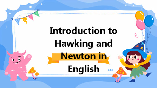
Introduction to Hawking and Newton in English
目录
• Introduction • Stephen Hawking • Isaac Newton • The similarities between Hawking and Newton • The Differences between Hawking and
Main achievements
Formulated the laws of motion, which describes the relationship between force, acceleration, and mass
科学现象英文面试题目(3篇)

第1篇Introduction:Quantum entanglement, one of the most intriguing and challenging concepts in quantum mechanics, has puzzled scientists for over a century. This phenomenon, where particles become interconnected regardless of the distance separating them, has far-reaching implications for our understanding of the universe and potential technological advancements. In this interview question, we will delve into the scientific principles of quantum entanglement, its experimental validations, and the potential applications it may offer in the future.Section 1: Introduction to Quantum Entanglement1.1 Definition of Quantum Entanglement:Quantum entanglement is a physical phenomenon that occurs when pairs or groups of particles become linked in such a way that the quantum stateof each particle cannot be described independently of the state of the others, even when the particles are separated by large distances.1.2 Historical Background:The concept of quantum entanglement was first introduced by Albert Einstein, Boris Podolsky, and Nathan Rosen in 1935 in their famous paper titled "Can Quantum-Mechanical Description of Physical Reality Be Considered Complete?" This paper, often referred to as the EPR paradox, sparked a debate on the completeness and interpretation of quantum mechanics.1.3 Quantum Mechanics and Classical Mechanics:Quantum entanglement is a quintessential feature of quantum mechanics, which fundamentally differs from classical mechanics. In classical mechanics, the state of a system is determined by the positions and velocities of its particles, while in quantum mechanics, particles exist in a probabilistic state until measured.Section 2: The Principles of Quantum Entanglement2.1 Superposition:Superposition is a fundamental principle of quantum mechanics, which states that a quantum system can exist in multiple states simultaneously. This principle allows particles to be entangled, as their combined state cannot be described by the state of each particle individually.2.2 Non-locality:Non-locality is the idea that quantum entangled particles can instantaneously affect each other's states, regardless of the distance separating them. This concept challenges the principle of locality in classical physics, which dictates that no physical influence can travel faster than the speed of light.2.3 Bell's Inequality:John Bell proposed an inequality in 1964 that sets a limit on the amount of non-local correlations that can exist between particles in classical physics. Quantum entanglement violates Bell's inequality, providing experimental evidence for the non-local nature of quantum mechanics.Section 3: Experimental Validations of Quantum Entanglement3.1 Alain Aspect's Experiment:In 1982, Alain Aspect conducted a groundbreaking experiment that confirmed the violation of Bell's inequality, providing strong evidence for quantum entanglement and non-locality. His experiment involved measuring the polarizations of photons emitted from a source and showed that the correlations between the photons exceeded the limits set byBell's inequality.3.2 Quantum Key Distribution (QKD):Quantum key distribution is a secure communication protocol that leverages the principles of quantum entanglement. It allows two parties to share a secret key with the guarantee that any eavesdropping can be detected. QKD has been experimentally demonstrated over long distances, such as satellite-based communication links.3.3 Quantum Computing:Quantum entanglement is a crucial resource for quantum computing, which aims to solve complex problems much faster than classical computers. Quantum computers use qubits, which are entangled particles, to perform calculations by exploiting superposition and interference.Section 4: Implications for Future Technologies4.1 Quantum Communication:Quantum entanglement has the potential to revolutionize communication by enabling secure, long-distance communication using QKD. This technology could be crucial for establishing secure networks and protecting sensitive information.4.2 Quantum Computing:Quantum entanglement is essential for the development of quantum computers, which have the potential to solve complex problems in cryptography, material science, and optimization. Quantum computers could also simulate quantum systems, leading to new discoveries in chemistry, physics, and biology.4.3 Quantum Sensing:Quantum entanglement can be used to enhance the sensitivity of quantum sensors, which have applications in various fields, including gravitational wave detection, quantum metrology, and precision measurement.Conclusion:Quantum entanglement, with its fascinating principles and experimental validations, has the potential to reshape our understanding of the universe and enable groundbreaking technological advancements. From secure communication to powerful quantum computers, the implications of quantum entanglement are vast and far-reaching. As scientists continue to explore this intriguing phenomenon, we can expect even more exciting developments in the field of quantum physics and its applications.第2篇Introduction:Quantum entanglement, one of the most fascinating and enigmatic phenomena in the realm of physics, has intrigued scientists and philosophers alike for decades. This interview delves into the depths of quantum entanglement, exploring its origins, implications, and potential applications. Dr. Emily Newton, a renowned quantum physicist, shares her insights and experiences in this field.Part 1: The Basics of Quantum EntanglementQuestion 1: Can you explain what quantum entanglement is and how it differs from classical entanglement?Dr. Newton:Quantum entanglement is a phenomenon in which two or more particles become interconnected, such that the quantum state of one particle instantaneously correlates with the state of another, regardless of the distance separating them. This correlation persists even when the particles are separated by vast distances, which defies the principles of classical physics.In classical entanglement, such as the entanglement of a pair of dice, the outcome of one die is independent of the other. If you roll a six on one die, it does not affect the outcome of the other die. However, in quantum entanglement, the particles are not independent; their quantum states are correlated in such a way that measuring one particle's state instantly determines the state of the other particle, regardless of the distance between them.Question 2: How was quantum entanglement discovered, and what were the early reactions to this phenomenon?Dr. Newton:Quantum entanglement was first predicted by Albert Einstein, Boris Podolsky, and Nathan Rosen in their famous EPR paradox paper in 1935.They proposed a thought experiment involving two entangled particlesthat seemed to violate the principle of locality, which states that no information can travel faster than the speed of light.The initial reaction to the EPR paradox was skepticism, with Einstein famously dismissing quantum entanglement as "spooky action at a distance." However, subsequent experiments, such as those conducted by John Bell in the 1960s, provided strong evidence in favor of quantum entanglement, leading to a paradigm shift in our understanding of the quantum world.Part 2: The Mechanics of Quantum EntanglementQuestion 3: What are the key factors that contribute to the formation of entangled particles?Dr. Newton:The formation of entangled particles is a result of their interaction during the process of measurement or preparation. For example, when two particles are created together in an entangled state, their quantum states become correlated due to their shared history. This correlationis a fundamental aspect of quantum mechanics and cannot be explained by classical physics.Another way to create entangled particles is through a process called entanglement swapping, where two particles are initially entangled with a third particle, and then the third particle is separated from thefirst two. This results in the first two particles becoming entangled with each other, even though they have never interacted directly.Question 4: Can you explain the concept of quantum superposition and how it relates to entanglement?Dr. Newton:Quantum superposition is the principle that a quantum system can existin multiple states simultaneously until it is measured. This is analogous to a coin spinning in the air, which can be either heads or tails until it lands on one side.In the context of entanglement, superposition plays a crucial role. When two particles are entangled, their combined quantum state is a superposition of the individual states of each particle. This means that the particles can exhibit non-local correlations that are not determined until a measurement is made.Part 3: The Implications of Quantum EntanglementQuestion 5: How does quantum entanglement challenge our understanding of the universe?Dr. Newton:Quantum entanglement challenges our classical understanding of the universe in several ways. Firstly, it defies the principle of locality, which has been a cornerstone of physics for centuries. The idea that particles can instantaneously influence each other across vast distances suggests that the fabric of space-time may not be as fixed as we once thought.Secondly, quantum entanglement raises questions about the nature of reality itself. If particles can be correlated in such a way that their states are instantaneously connected, it challenges the idea that objects have definite properties independent of observation.Question 6: Are there any practical applications of quantum entanglement?Dr. Newton:Yes, there are several potential applications of quantum entanglement. One of the most promising is in quantum computing, where entangled particles can be used to perform complex calculations at speeds unattainable by classical computers. Quantum entanglement is also essential for quantum cryptography, which can be used to create unbreakable encryption methods.Moreover, entanglement has been used in quantum teleportation, where the state of a particle can be transmitted instantaneously from one location to another, potentially leading to new communication technologies.Conclusion:Quantum entanglement remains one of the most intriguing and challenging phenomena in physics. Dr. Emily Newton's insights into the mechanics and implications of this phenomenon provide a deeper understanding of the quantum world and its potential applications. As we continue to explore the mysteries of quantum entanglement, we may uncover new ways to harness its power and reshape our understanding of the universe.第3篇IntroductionQuantum entanglement, one of the most intriguing and mysterious phenomena in the field of quantum mechanics, has captured the imagination of scientists and the public alike. This question invites candidates to delve into the concept of quantum entanglement, its underlying principles, experimental demonstrations, and the potential implications it holds for future technology.Part 1: Introduction to Quantum Entanglement1.1 Definition and Basic PrinciplesQuantum entanglement refers to a phenomenon where two or more particles become interconnected in such a way that the quantum state of each particle cannot be described independently of the state of the others, even when they are separated by large distances. This correlation persists regardless of the distance between the particles, which challenges our classical understanding of locality and separability.1.2 Historical ContextThe concept of quantum entanglement was first introduced by Albert Einstein, Boris Podolsky, and Nathan Rosen in their famous EPR paradox paper in 1935. They described entanglement as "spooky action at a distance," suggesting that it defied the principles of local realism. However, subsequent experiments and theoretical developments have confirmed the reality of entanglement.Part 2: Theoretical Underpinnings of Quantum Entanglement2.1 Quantum SuperpositionQuantum superposition is a fundamental principle of quantum mechanics that allows particles to exist in multiple states simultaneously. This principle is crucial for understanding entanglement, as it enables particles to become correlated in a way that is not possible inclassical physics.2.2 Quantum Correlation and EntanglementQuantum entanglement arises from the non-classical correlations between particles. When particles become entangled, their quantum states become linked, and the state of one particle instantaneously influences the state of the other, regardless of the distance separating them.2.3 Bell's TheoremJohn Bell formulated a theorem in 1964 that demonstrated the incompatibility of quantum mechanics with local realism. Experimentsthat violate Bell's inequalities have confirmed the existence of quantum entanglement and its non-local nature.Part 3: Experimental Demonstrations of Quantum Entanglement3.1 Bell Test ExperimentsBell test experiments have been conducted to test the predictions of quantum mechanics and to demonstrate the non-local nature of entanglement. These experiments involve measuring the properties of entangled particles and analyzing the correlations between them.3.2 Quantum Key Distribution (QKD)Quantum Key Distribution is a protocol that uses quantum entanglement to securely transmit cryptographic keys. It takes advantage of theprinciple that any attempt to intercept the entangled particles will disturb their quantum state, alerting the communicating parties to the presence of an eavesdropper.3.3 Quantum TeleportationQuantum teleportation is the process of transmitting the quantum state of a particle from one location to another, without the particle itself traveling through the space between them. This phenomenon has been experimentally demonstrated and has implications for quantum computing and communication.Part 4: Implications for Future Technology4.1 Quantum ComputingQuantum computing, which relies on the principles of quantum mechanics, has the potential to revolutionize computing by solving certain problems much faster than classical computers. Quantum entanglement plays a crucial role in quantum computing, as it allows for the creation of qubits that can exist in multiple states simultaneously, enabling parallel processing.4.2 Quantum CommunicationQuantum communication utilizes the principles of quantum entanglement and superposition to achieve secure communication and distributed computing. Technologies like QKD and quantum teleportation are expected to transform the field of secure communication and enable new forms of data transmission.4.3 Quantum Sensors and MetrologyQuantum sensors and metrology techniques leverage the precision and sensitivity of quantum entanglement to measure physical quantities with unprecedented accuracy. This has applications in fields such as precision navigation, gravitational wave detection, and quantum simulation.ConclusionQuantum entanglement, with its counterintuitive nature and profound implications, remains a captivating and challenging subject in the field of quantum mechanics. As scientists continue to explore and harness thepower of entanglement, we can expect to see significant advancements in technology, leading to new possibilities in computing, communication, and metrology. This question has provided an opportunity to delve into the fascinating world of quantum entanglement and its potential future impact on society.。
苹果大楼新总部 (norman Forster)

美国,旧金山,Cupertino市,苹果公司新园区/福斯特事务所乔布斯的苹果公司的新园区,由福斯特事务所、ARUP美国公司和一家本地的Kier & Wright工程公司一同设计。
它靠近苹果现有的园区,与硅谷的其它公司,如eBay, Nvidia, Cisco, Netflix and Sun近邻。
该园区的功能如下:办公,研究,面积大约280万平方英尺,可容纳13000雇员,1000座位的会议厅,中心绿地。
相应的停车位。
它是一个令人着迷的建筑。
它像一个着陆的宇宙飞船。
它的中心帅称宽阔的内院。
这样的建筑并不便宜,它没有一块玻璃是平的,我们事务所在世界各地都有建成的建筑,我们能找到建筑用的最大的玻璃,我们想通过这种方式让建筑独特,这非常酷。
圆形有利于园区的安全保卫,也能促进内部的交流。
该项目通过产生电力来减低能耗。
为苹果公司的雇员们提供中央的开放绿地。
通过精心的设计,超越了经济社会和环境的局限。
乔布斯选择了正确的设计事务所。
从图纸上看,该项目正在等待城市当局审批,该项目很可能获得批准,可能于2015年落成。
原文:The city of Cupertino has released more details about the new Apple Campus, revealed back in June.The new documents confirm Foster + Partners as the architects, working with ARUP North America and Kier & Wright, a local civil engineering firm that has worked on Apple’s current campus and buildings for other tech companies (eBay, Nvidia, Cisco, Netflix and Sun, among others).About the program:An Office, Research and Development Building comprising approximately 2.8 million square feet for up to 13,000 employeesA 1,000 seat Corporate AuditoriumA Corporate Fitness CenterResearch Facilities comprising approximately 300,000 square feetA Central PlantAssociated ParkingIt’s a pretty amazing building. It’s a little like a spaceship landed. It’s got this gorgeous courtyard in the middle… It’s a circle. It’s curved all the way around. If you build things, this is not the cheapest way to build something. There is not a straight piece of glass in this building. It’s all curved. We’ve used our experience making retail buildings all over the world now, and we know how to make the biggest pieces of glass in the world for architectural use. And, we want to make the glass specifically for this building here. We can make it curve all the way around the building… It’s pretty cool.The round shape has also been cited as an important part of the campus’ security (better perimeter control) and to improve internal circulations.It’s interesting to see that the objectives of the project are focused on reducing the use of electricity by generating its own energy on an on-site Central Plant, provide open green spaces “for Apple employees’ enjoyment” and to “exceed economic, social, and environmental sustainability goals through integrated design and development”. It seems Jobs choose the right firms for this.By looking at the drawings it seems that the project is ready to go, and now it’s waiting for city approval. The city has revealed that they are very likely to approve the project, so it seems everything is on route for an opening in 2015.。
0000_材料专业英语_Semiconductors_an_Introduction

Semiconductors:An IntroductionA crucial feature of the quantum-mechanical band theory of solids is that electrons in a crystal of any given material occupy well-defined quantum states, with discrete momentum and energy values(Kittel 1996)The interactions that arise between the different atoms in the crystal result in the grouping of these states into bands of allowed energies,with successive bands being separated from each other by forbidden energy gaps.Within this picture,the manner in which the valence electronsfill the energy bands is critical to understanding the electrical properties of the crystal.Metals are materials in which the uppermost energy band is only partially filled with electrons(Fig.1),and exhibit high conductivity since electrons may easily be accelerated into new momentum states by the application of even a small electricfield.Insulators,on the other hand,are materials in which the uppermost energy band is(almost) completelyfilled with electrons,and is separated from the lowest band of empty states by a large energy gap(in excess of several electron volts,Fig.1). These materials exhibit poor conductivity,since the large energy gap that separates the valence band(the highestfilled band at low temperatures)from the conduction band(the lowest unfilled band at low temperatures)blocks the acceleration of electrons into new momentum states.A group of materials whose properties are intermediate between these two extremes is referred to as semiconductors.Thefilling of electron states in semiconductors is similar to that in insulators,except the valence and conduction bands are separated by a smaller energy gap,of order1–2eV.At absolute zero,their valence band is completelyfilled with electrons,while the conduction band is empty,and the electrical char-acteristics are therefore similar to those of insulators. With increasing temperature,however,increasing numbers of electrons are thermally excited across the energy gap,into the conduction band,and the conductivity increases(Fig.1).Since the number of electrons in the conduction band increases exponen-tially with temperature(see the discussion below),the conductivity of these materials exhibits very strong temperature dependence.The existence of the forbidden energy gap in semiconductors has allowed the development of a variety of optoelectronic devices,among which include light-emitting diodes,photodetectors,and solar cells,and diode and heterojunction lasers. Another critical feature of these materials is that, unlike in metals,their electrical properties may be modified over a wide range of parameter space by the controlled addition of impurities known as dopants.In pure silicon at room temperature,the intrinsic carrier concentration is approximately 1010cmÀ3,and may easily be varied by many orders of magnitude by doping with the appropriate impurity.Moreover,simply through the choice of dopant,it is possible to realize semiconductor systems in which the majority carriers are either negatively charged electrons,or positively charged holes.Thisflexibility in turn allows the realization of a range of novel,nonlinear,semiconductor devices, such as pn junctions,field-effect transistors(MOS-FETs and MESFETs),and bipolar junction transis-tors,and provides the basis for modern low-power (CMOS)electronics.The purpose of this article is to review the key concepts required for understanding the electrical properties of semiconductors.We begin with a discussion of the different types of semiconductors, their crystal structures,and their energy gaps.After this,we explain the bandstructure details of selected semiconductors(Si and GaAs),followed by a brief discussion of semiconductor statistics.It is here that we introduce the concept of holes as another source of charge carriers in semiconductors.In Sect.4,we discuss how doping may be utilized to modify the intrinsic carrier concentrations in semiconductors, and a brief summary is given in Sect.5.1.Elemental and Compound Semiconductors Broadly speaking,semiconductors may be divided into two distinct groups,namely elemental or compound semiconductors.As the name suggests,elemental semiconductors are formed from single chemical elements,and important members of this family include Si and pound semiconductors represent the largest group,however,and are formed as a result of the chemical reaction between two or more different elements (examples include GaAs,InAs,InP,and GaN).Another important group of materials is provided by semiconductor alloys ,among which include Al x Ga 1Àx As and Si 1Àx Ge x .These materials are compound semiconductors in which the atoms are arranged in a well-defined crystal structure,but in which the different chemical species are randomly distributed throughout this crystal.While the bonding in most semiconductors is largely covalent in nature,in compound semiconductors formed from elements other than those in Group IV of the periodic table,the bonding also exhibits a small ionic nature and the material is said to be polar (Ferry 1991).Elemental semiconductors,on the other hand,are referred to as nonpolar .Crystal structure plays an important role in determining the bandstructure,and the resulting electrical properties,of semiconductors.The vast majority of these materials exhibit either the diamond or the zincblende crystal forms (Fig.2),the under-lying lattice of which is the face-centered cubic lattice.In a compound semiconductor,such as GaAs,the two atoms in the basis are from different chemical species and this is known as the zincblende form.In either case,hybridization of the outermost occupied s -and p -orbitals gives rise to a tetrahedral bondingarrangement in the crystal (Ferry 1991)(Fig.2),in which each atom bonds to its four nearest neighbors,forming a tetrahedral structure with the center atom located at the body of the tetrahedron.While the diamond and zincblende structures account for the majority of semiconductors encoun-tered in nature,a less common form is the wurtzite structure.This is essentially based on the hexagonal lattice.The tetrahedral bonding arrangement remains in this crystal form,and GaN is an important example of a semiconductor that can exhibit the wurtzite structure.The crystal structure,and value of the principal energy gap ðE g Þ,of a number of different semiconductors are summarized in Table 1.The form of the principal gap (direct versus indirect)is also shown in this table,although we defer a discussion of this issue until Sect.2.1.2.Semiconductor BandstructureBandstructure diagrams are the key to understanding the electrical and optical properties of semiconduc-tors.These diagrams show the relationship between the electron energy and momentum,for different principal directions within the crystal.(Strictly speaking,the diagrams show the variation of the energy with electron wave vector k ,which is in turn related to the crystal momentum ,_k .See Singh (1993)for example.)While a number of techniques are available for the calculation of bandstructures,these approaches may be broadly divided into two groups.The first group consists of methods which compute the bandstructure of the entire conduction and valence bands,and an important example of such an approach is provided by the tight-binding method .Figure 2Illustrations of the unit cell in the diamond (left)and zincblende (right)crystal structures.The solid lines between atoms in both figures represent chemical bonds.Note that,for the sake of clarity,chemical bonds extending outside the unit cell are not shown.In the case of the zincblende structure,the different colored balls represent atoms from different chemical species (for example,Ga and As in GaAs).2Semiconductors:An IntroductionThis starts from the orbital wave functions of the individual atoms,and computes the electron energy by considering the interaction of a center atom with its neighbors.The simplest approach is to consider only nearest-neighbor interactions,although higher accuracy can be achieved by extending this model to account for next-nearest neighbor interactions as well.The other group of bandstructure calculations consists of methods which only describe the bandstructure close to the edge of the energy gaps.The advantage of such approaches,among which include the kÁp method,is a reduction in the complexity of the problem,and an accurate description of the energy bands near the principal gaps can be achieved.This simplicity is achieved at the cost of generality,however,since it is not possible to extend such approaches over a wide range of parameter space.For detailed discussions of bandstructure-calculation approaches in semiconduc-tors,we refer the interested reader to books by Ferry (1991),Yu and Cardona(1996),Singh(1993),Ferry (2000),and Hamaguchi(2001).We have mentioned that bandstructure diagrams show the relationship between the electron energy and momentum for different principal directions within the crystal.These directions are defined in terms of the reciprocal lattice,which may be viewed as the Fourier transform of the real-space lattice of the crystal.Since the semiconductors of interest hereexhibit either the diamond or zincblende structures,it is worthwhile to take a few moments to consider the definition of the principal axes for these crystals.As was mentioned already,both of these structures are formed on the face-centered cubic lattice,the reciprocal lattice of which is the body-centered cubic lattice(Kittel1996).In Fig.3,we show thefirst Brillouin zone for the body-centered cubic lattice, and indicate the terminology used to identify the important directions of the reciprocal lattice.The surface of the Brillouin zone contains all electron wave vectors for which the Bragg condition for diffraction from some particular family of crystal planes is satisfied,and so for which an energy gap is expected in the bandstructure.The various points identified in Fig.3are of importance since they indicate directions of high crystal symmetry.2.1Silicon BandstructureIn Fig.4,we show the computed bandstructure diagram for Si.There are a number of important general features in this diagram that are worthy of emphasis.To begin with,on the horizontal axis,the variation of energy with wave vector is plotted as we start at the L point in the Brillouin zone,and then progress to the G,X,and U points,beforefinally returning to the G point.Next,we note that the series of curves shown in Fig.4may be roughly grouped into two sets of four,separated by a forbidden-gap region(shaded area),where no electron states are available.The reason for this grouping is quite simpleTable1Key semiconductors,their crystal structure,and energy-gap values.Note that the other form of C is graphite, which exhibits a hexagonal crystal structure and is a semimetal.Semiconductor Crystalstructure Gap type Energy gap(E g)at300K(eV)Si Diamond Indirect 1.124C Diamond Indirect 5.50SiC Zincblende Indirect 2.416Ge Diamond Indirect0.664AlN Wurtzite Direct 6.2AlP Zincblende Indirect 2.45AlAs Zincblende Indirect 2.153AlSb Zincblende Indirect 1.615GaN Wurtzite Direct 3.44GaP Zincblende Indirect 2.272GaAs Zincblende Direct 1.424GaSb Zincblende Direct0.75InAs Zincblende Direct0.354InSb Zincblende Direct0.230CdS Zincblende Direct 2.50CdSe Wurtzite Direct 1.751CdTe Zincblende Direct 1.475Source:Madelung(1996),Pierret(1996).Figure3Thefirst Brillouin zone of the face-centered cubic lattice.The various symbols are used to denote directions ofhigh symmetry in the crystal.3Semiconductors:An Introductionto understand;in the tight-binding model,the energy is calculated from a knowledge of the atomic wave functions,in particular the wave functions of the valence electrons.In practice,these wave functions are the s-and p-orbitals,and,with two atoms in the basis of the diamond or zincblende structures,a total of eight wave functions are used as the basis set for the calculations.The interaction between the orbitals on different atoms gives rise to a hybridization,as a result of which both the valence and the conduction bands exhibit s-orbital-like and p-orbital-like nature. In particular,it may be shown that the top of the valence band is predominantly derived from the p-type orbitals,while the bottom of the conduction band at G is largely s-orbital derived.This difference has important implications for the bandstructure near the top of the valence band,where the nonzero spin-orbit interaction of the p-like electrons lifts the degeneracy of the valence band at the G point.This effect is shown in greater detail in Fig.5,where we show how the spin-orbit effect gives rise to the split-off valence band.Note that there is usually no spin-splitting at the bottom of the conduction band,since these electron states are predominantly s-like in nature,and so are characterized by zero angular momentum.(A splitting of the conduction band can arise due to the effects of bulk-inversion asymmetry in polar crystals,although this effect is typically small in most semiconductors(Lommer et al.1988).)Si is an indirect semiconductor,since the maximum in its valence band and the minimum in its conduc-tion band are located at different wave vectors.The valence-band maximum is located at the G point, while the minimum in the conduction band is located about85%of the way towards the X point(see Fig.4).Due to the symmetry of theface-centered Semiconductors:An Introductioncubic lattice,six equivalent X points may be identified.At least for reasonably small variations of the wave vector away from the X point,the energy variation may be assumed to be parabolic and may be written in terms of two effective masses:E ¼_2k 2x2m L þ_2ðk 2y þk 2z Þ2m Tð1ÞHere,m n L and m nT are the longitudinal and transverse effective masses,respectively.In terms of the free electron mass,m o ,it is found that m n L ¼0:91m o and m nT ¼0:19m o .For a given reference energy for which Eqn.(1)is valid,we may therefore identify six constant energy surfaces ,which are centered around the X point (Fig.6).The asym-metric,cigar-like shape of these energy surfaces reflects the difference,noted above,in the long-itudinal and transverse effective masses near the X point.As we discuss in more detail below,at room temperature,electrons in semiconductors tend to lie close to the bottom of the conduction band,and in Si this leads to the ‘‘puddling’’of electrons in the six conduction-band minima.The cigar-like features shown in Fig.6may therefore be viewed as repre-senting the occupation of electron states in the conduction band of Si. 2.2Gallium-Arsenide BandstructureIn Fig.7,we show the computed bandstructurediagram for GaAs.There are some important differences with the bandstructure of Si,probably the most important of which is that GaAs is a direct semiconductor;the maximum in its valence band and the minimum in its conduction band are located at the same points in reciprocal space.Close to the bottom of the conduction band,the variation of the energy with wave vector may be approximated as:E ¼_2k 22m nð2Þwhere the electron effective mass is isotropic and takes the value m n ¼0:067m o .Another important feature of the bandstructure is the presence of satellite valleys in the conduction band,which are the local minima located at the X and L points (in Fig.7).The effective mass is very different in these valleys,from the usual electron mass in the minimum near the G point,and a dramatic reduction in mobility results when electrons are accelerated to sufficient energy by an applied electric field,to scatter into these satellite valleys.As can be seen in Fig.8,the spin-splitting of the valence band is significantly larger in GaAs than in Si.The separation of the split-off band from the top of the valence band is denoted by D so ,and in Si the value of this parameter is 44meV,while in GaAs it is 350meV.It is for this reason that the split-off band plays little role in transport inGaAs.Figure 6Constant-energy ellipsoids in silicon,associated with the six-fold-degenerate minimum in the conduction band.5Semiconductors:An Introduction2.3Some General Comments on Bandstructure(a)Energy gaps .The energy gaps listed in Table 1are the principal energy gaps for the different materials,that is they are the smallest energy gaps that separate the top of the valence band from the bottom of the conduction band.The relative location of the maximum and minimum in k -spaceisFigure 8A comparison of the valence bandstructure of GaAs and Si,showing that spin-orbit coupling leads to a larger splitting of the valence band in GaAs than in Si (reproduced from Hamaguchi 2001with permission).6Semiconductors:An Introductionimportant for determining the optical properties of semiconductors.In indirect semiconductors,the maximum and minimum occur at different points in k-space and direct transitions from the conduction band to the valence band have low probability.The reason for this is that when an electron drops from the conduction band to the valence band,and releases its excess energy in the form of a photon, the crystal momentum must be conserved.(We should remember that crystal momentum is only defined to within an arbitrary reciprocal-lattice wave vector.See K ittel1996,for example.)While the photon may carry a large amount of energy,its momentum relative to that of the electron is very small.Thus,the transition of the electron should leave its wave vector almost unchanged from its initial value—a requirement that cannot be satisfied in an indirect semiconductor.Here,a large change in crystal momentum is associated with a transition between the conduction-band maximum and the valence-band minimum,and this must be taken up by the simultaneous emission or absorption of a phonon.Since this photon–phonon emission has a low probability,indirect materials,such as Si,are poor choices for optical emitters.The energy gap of semiconductors varies weakly with temperature,typically decreasing with increas-ing temperature.In Si,for example,the size of the energy gap decreases by about0.07eV when the temperature is increased from20to400K.This corresponds to a relative change of roughly6%, compared to the value of the room-temperature gap (Madelung1996).There are a number of processes that contribute to the temperature-dependent varia-tion of the bandgap(Ridley1999),one of which is thermal expansion of the crystal.This weakens the overlap integrals of the orbitals on the different atoms,and so reduces the energy hybridization resulting from the overlap.Another effect is a thermal smearing of the background periodic poten-tial,created by the atom cores in the crystal.These effects may be accounted for by considering the influence of temperature on the electron–phonon interaction,which provides a contribution to the total energy of electrons in the crystal.The important point is that the process of exciting electrons into the conduction band corresponds to the breaking of bonds in the crystal,which in turn‘‘softens’’the vibrational modes of the atoms,by weakening the elastic restoring forces exerted between them.By lowering the energy of the vibrational modes in this manner,it is possible to show that the size of the bandgap is reduced with increasing temperature (Ridley1999).(b)Conduction and valence-band effective masses. Within the context of band theory,the effective mass of carriers in a crystal is understood to be related to the curvature of their energy bands in k-space.The starting point of this discussion is the expression for the crystal momentum of an electron in the crystal. Considering,for ease of development,a one-dimen-sional problem,the crystal momentum may be written as:p¼_k¼m n v gð3Þwhere m n is the electron effective mass and v g is the electron group velocity.This latter quantity may be written as:v g¼1_d Eð4ÞBy combining Eqns.(3)and(4)we thus arrive at the following expression for the effective mass(Ferry 2000):1m n¼1_kd Ed kð5ÞWe see from Eqn.(5)that the effective mass is related to the gradient of the energy bands in k-space,as mentioned just above.(The reader may be more used to the expression1=m n¼ð1=_2Þðd2E=d k2Þ,but this is only valid for parabolic bands!Eqn.(5)represents a more general form for the effective mass that is valid for any dispersion of E with k.We refer the reader to Ferry(2000)for a more detailed discussion of this point.)In Fig.9,we illustrate schematically the typical bandstructure of a semiconductor near its energy gap.The k-space origin in thisfigure corresponds to the G point,which is a high point of symmetry for the crystal.In the absence of spin-orbit coupling,the top of the valence band is expected to be three-fold degenerate,since this portion of the bandstructure is derived from the p-type orbitals,which are three-fold degenerate in the absence of any magnetic interac-tion.Spin-orbit coupling lifts this degeneracy,how-ever,by lowering the energy of the split-off band relative to the other two components(see Fig.9).The top of the valence band is then left two-fold degenerate at the G point,and we refer to these bands,which typically exhibit different degrees of curvature,as the light-and heavy-hole bands.Values of the valence-band effective masses are listed for a few semiconductors in Table2.While spin-orbit coupling typically leaves the conduction-band edge unaffected,we have seen that in indirect semiconductors,such as Si,it is necessary to introduce multiple effective masses,which compli-cates the calculation of physical quantities depen-dent on the effective mass.In Si,for example, one defines the density of states effective mass, m nd62=3ðm*2T m n LÞ1=3¼1:08m o.As we will see,this mass is used in the density of states to calculate the occupation of electron states atfinite temperatures.It7Semiconductors:An Introductionis also possible,however,to define the conductivity effective mass ,which is used in calculations of the electrical properties.To determine this mass,we note that,with the electric field applied in a particular direction,two valleys will exhibit the longitudinal mass while the other four will exhibit the transverse mass.The conductivity mass is then defined as (Ferry 1991):1n c ¼14T þ2L ¼1oð6ÞAnother indirect semiconductor is germanium,which exhibits eight equivalent conduction-band minima,located at the L points in the Brillouin zone (see Fig.3).The ellipsoids are characterized by theeffective masses m n T ¼0:082m o and m nL ¼1:64m o ,and the density of states effective mass is givenby m n d 42=3ðm *2T m n L Þ1=3¼0:56m o .Note the factor of four,rather than eight,that appears in this expression;this results since only half of each ellipsoid is contained within the Brillouin zone.The conductivity mass for Ge can also be calculated using the principles discussed above,yielding m n c ¼0:12m o .In many semiconductors,there is typically a proportional scaling of the conduction-band effective mass with the size of the energy gap,as we illustrate for selected semiconductors in Fig.10.This figure shows that larger-gap semiconductors exhibit heavier masses,and this basic scaling can be accounted for within the k Áp method,which uses perturbation theory to expand the bandstructure around the G point.This approach yields a conduction-band effective mass that is predicted to vary as:1m n ¼1m o þ2p cv 3m o 2E g Gþ1E g G þD soð7ÞIn this equation p cv is a momentum matrix element (Singh 1993,Ferry 2000,Ridley 1999)involving the conduction-and valence-band wave functions,E g G is the bandgap measured at the G point,and D so is the magnitude of the valence-band spin splitting.In Fig.10we show that the conduction-band mass of many semiconductors follow the approximate scaling of mass with bandgap suggested by Eqn.(7).Table 2Valence-band effective masses for selectedsemiconductors;m n l ,m n h ,and m nso denote the effective mass for the light-,heavy-,and split-off-bands,respectively.Semiconductor m n l =m o m n h =m o m n so =m o Si 0.150.540.23Ge 0.0430.280.095GaAS 0.080.510.15GaP 0.170.670.46InAs 0.0260.400.14InP0.120.600.12Semiconductors:An Introduction3.Carrier Statistics in Semiconductors3.1Electrons and HolesAt absolute zero,the valence band in any semicon-ductor isfilled completely with electrons while its conduction band is empty.At this temperature,the semiconductor therefore behaves like an insulator, since the large energy gap that separates the highest filled electron states from the lowest empty ones makes it difficult to accelerate electrons by applying a modest electricfield.The difference between insula-tors and semiconductors becomes apparent when the temperature is increased above zero,however,and the thermal energy allows for the excitation of increasing numbers of electrons across the small forbidden gap of semiconductors into the conduction band.Under such conditions,currentflow through the semiconductor becomes possible and the con-ductivity of these materials increases with increasing temperature,as more electrons are excited into the conduction band(Fig.11).Now consider the situation where a single electron is excited from a completelyfilled valence band,into the conduction band,leaving behind an unfilled electron state in the valence band.The presence of this empty state has critical consequences for current flow,since electrons in the valence band may now also carry an electrical current,in addition to the electron excited into the conduction band.An issue that arises here,concerns how to describe theflow of current due to carriers in the valence band,and this discussion leads us to introduce the concept of holes. The basic idea is that,in the presence of an applied electricfield E(we once again consider a one-dimensional problem for simplicity),each electron state experiences the same change in wave number:D k¼Àe t_Eð8Þwhere t is the usual relaxation time and the minus sign reflects the negative charge of the electron.Instead of following how the electricfield affects the momentum of the large number of electrons in the almost-filled valence band,however,it is instead more convenient to consider what happens to the single unoccupied electron state.On the basis of the discussion above,it should be clear that the applied field must change the wave vector of this state by:D k¼þe t_Eð9Þwhere the positive sign means that the response now looks like that of a particle with a positive charge,þe. This positively charged particle is referred to as a hole,and we emphasize that this concept is simply introduced for convenience.This does not mean that electrons in the valence band somehow possess a positive charge.Rather,what we are saying is that with a single electron missing from the valence band, the collective response of the remaining electrons to an applied electricfield looks just like that which we would expect for a single positively charged hole. While we have thus far considered the case of a single electron promoted out of the valence band,the concept of holes remains useful even when we begin to excite larger numbers of electrons into the conduction band.As we will see below,calculations of the electrical properties of semiconductors there-fore typically require that we consider the influence of both electrons in the conduction band and holes in the valence band.(a)Energy scale for holes.We have introduced the concept of the hole as a positively charged quasipar-ticle,which is useful when describing the response of an almost-filled valence band to an applied electric field.The hole results when an electron is excited from the valence band into the conduction band, either by utilizing the available thermal energy in the system,or by an optical process in which the electron absorbs the energy of an incident photon.A comparison of Eqns.(8)and(9)indicates that the hole possesses a positive charge,þe.Another important feature to note is that holes possess an inverted energy scale,that is,moving down in the valence band corresponds to increasing hole energy. The simple example shown in Fig.12serves to clarify the reason for this inverted energy scale.In this figure,we consider the situation where we use a photon to excite an electron from the valence band to the bottom of the conduction band(denoted by E c in Fig.12).On the left-hand side of thisfigure,we show the case where the electron initially occupies a state at the top of the valence band(denoted by E v).On the right-hand side,however,the electron is excited from a state lying further down in the valence band.Since thefinal energy of the electron,after the photon is absorbed,is the same in both cases,it is clear that a photon with a larger energy is required to induce theSemiconductors:An Introduction。
- 1、下载文档前请自行甄别文档内容的完整性,平台不提供额外的编辑、内容补充、找答案等附加服务。
- 2、"仅部分预览"的文档,不可在线预览部分如存在完整性等问题,可反馈申请退款(可完整预览的文档不适用该条件!)。
- 3、如文档侵犯您的权益,请联系客服反馈,我们会尽快为您处理(人工客服工作时间:9:00-18:30)。
a r X i v :h ep-th/03529v214J ul23Center of quantum group in roots of unity and the restriction of integrable models The talk given in RAQIS03conference,Aneccy,25-28/03/03A.Belavin Landau Institute for Theoretical Physics,Chernogolovka,142432,Russia e-mail:belavin@itp.ac.ru February 1,2008Abstract We show the connection between the extended center of the quan-tum group in roots of unity and the restriction of the XXZ model.We also give explicit expressions for operators that respect the restric-tion and act on the state space of the restricted models.The formulas for these operators are verified by explicit calculation for third-degree roots;they are conjectured to hold in the general case.1IntroductionF.Alcaraz et al.[1]discovered a remarkable fact:the XXZ model with the special open boundary conditions (OBC)and a rational value of the anisotropy parameter admits a restriction.The model arising as a result of the restriction coincides in the thermodynamic limit with one of the Minimal Models of CFT.The algebraic reason for the restriction was explained in [2]and [3].It was shown in [2]that the XXZ model with the OBC considered in [1]has not only integrability but also U q (sl (2))symmetry.In roots of unity,the state space of the model decomposes to the sum of “good”and “bad”1representations of U q(sl(2)).The restriction of Alcaraz et al.is equivalent throwing out“bad”parts and keeping only the highest vectors of“good”representations.In[3],a new monodromy matrix was constructed that is bilinear in terms of generators of the quantum group A(u),B(u),C(u), D(u)connected in the usual way with the Hamiltonian of the model in[1] and compatible with integrability.The twisted trace of this monodromy matrix(Sklyanin transfer matrix)also has U q(sl(2))symmetry and admits the restriction.In this paper,we generalize the Pasqier–Saleur construction.We show that not only U q(sl(2))-invariant but also a much wider class of OBC indeed admits the restriction(the Sklyanin construction of the transfer matrix also works for this wider class of OBC).The decisive condition for compatibility of the Hamiltonian,the transfer matrix,and other operators with the restiction is their“weak”commutativity with a special element of the quantum group. The notion of“weak”commutativity and its connection with the extension of the center of the quantum group in roots of unity is explained below.In Sec.2,we describe the conditions that the operators must have in order to admit the restriction.In Sec.3,some such operators are found.We discuss some possible generalizations of the construction in the last section. 2Center of the quantum group and the re-striction in roots of unityAs usual,let the R-matrix R(u)denote the solution of the Yang–Baxter equa-tion.We consider the simplest and well-known R(u)matrix corresponding to the six-vertex model,whose elements can be written asRαααα(u)=ρsin(u+η),Rαβαβ(u)=ρsin u,Rαββα(u)=ρsinη,(1)whereα,β=1,2,α=β,andηis the so-called anisotropy parameter.The quantum group A connected with R(u)is generated by A(u),B(u), C(u),D(u),entries of the monodromy matrix L(u),which satisfiesR12(u−v)L1(u)L2(v)=L2(v)L1(u)R12(u−v).(2)2As shown by V.Tarasov[4],the center of A in roots of unity,i.e.,η=πm/N, is generated by the following elements of A:A(u) =A(u)A(u+η)···A(u+(N−1)η),B(u) =B(u)B(u+η)···B(u+(N−1)η),C(u) =C(u)C(u+η)···C(u+(N−1)η),D(u) =D(u)D(u+η)···D(u+(N−1)η).For convenience,we let B(u) denote the central element,B(u) =B(u)B1(u),whereB1(u)=B(u+η)···B(u+(N−1)η).We nowfix V=C2⊗···⊗C2as the representation space of our quantum group.It is easy to see that for arbitrary v,B(v) =B(v)B1(v)=0on this space.We can then define the state space of a restricted model asW(v)=Ker B(v)/Im B1(v).In the limit v→∞,B(v)coincides up to a scalar factor with X,one of the generators of U q(sl(2)).As a result,W(∞)coincides with the space of the“good”highest vectors of Pasqier–Saleur.It was shown in[2]that the Hamiltonian of the XXZ chain with OBC of special typeH XXZ=L−1n=1 σ+nσ−n+1+σ−nσ+n+1+cosη2(σz n−σz n+1)is invariant under the quantum algebra U q(sl(2)).Here,q=eη.Because of this,H XXZ is properly defined on W(∞)=Ker X/Im X(N−1).In the thermodynamic limit,where L→∞,the spectrum of low-lying states coincides(in Cardy’s sense)with M(N−1/N),one of the Minimal Models of CFT.In the next section,we show that the construction in[2]can3be generalized to arbitrary values of the parameter v.The corresponding Hamiltonian is[3],[5]H XXZ=L−1n=1 σ+nσ−n+1+σ−nσ+n+1+cosη2(cot vσz1−cot(v+η)σz L).(3)We nowfind the sufficient conditions for any operator Q to be projectible on W(v).It is easy to see that sufficient conditions are that there exist some operators Q and Q1for a given Q such thatB(v)Q= QB(v)(4) andQB1(v)=B1(v) Q1.(5) Indeed,Eq.(4)guarantees that if a vectorψ∈Ker B(v),then the vector Qψ∈Ker B(v).It follows from Eq.(5)that if the difference of two vectors ψ1andψ2belong to Im B1(v),i.e.,ifψ1−ψ2=B1(v)χ,then the difference of Qψ1and Qψ2also belongs to Im B1(v).3Sklyanin transfer matrix and other opera-tors respecting the restriction in roots of unityIn[3],E.Sklyanin explained the integrability of the XXZ model with OBC of the formH XXZ=L−1n=1 σ+nσ−n+1+σ−nσ+n+1+cosη2(cot(ξ++η/2)σz1+cot(ξ−−η/2)σz L).by constructing a special monodromy matrix and using it to diagonalize Hamiltonian(3)and the corresponding transfer matrix by means of the al-gebraic Bethe ansatz.4Let K+(u)=K(u+η/2,ξ+)and K−(u)=K(u−η/2,ξ−),whereK(u,ξ)= sin(u+ξ)00−sin(u−ξ) .Then K±satisfies the boundary Yang–Baxter equations[3],[6].The Sklyanin monodromy matrix is defined[3]asΛ(u)=σ2L t(−u)σ2K+(u)L(u)= Λ11Λ21Λ12Λ22 .Using(2)and the boundary Yang–Baxter equation,we can prove thatΛ(u) satisfies the same equation as K+(u).It gives the commutation relations betweenΛi j.The Sklyanin transfer matrix is defined asT S(u)=trΛ(u)K−(u)=sin(u−η/2+ξ−)Λ11−sin(u−η/2−ξ−)Λ22.Explicit expressions for the elements of the Sklyanin monodromy matrix areΛ11(u)=sin(u+η/2+ξ+)A(u)D(−u)+sin(u+η/2−ξ+)C(u)B(−u),Λ22(u)=−sin(u+η/2+ξ+)B(u)C(−u)−sin(u+η/2−ξ+)D(u)A(−u),Λ21(u)=sin(u+η/2+ξ+)B(u)D(−u)+sin(u+η/2−ξ+)D(u)B(−u),Λ12(u)=−sin(u+η/2+ξ+)A(u)C(−u)−sin(u+η/2−ξ+)C(u)A(−u).Letξ+=v−η/2andξ−=−v−η/2.Then the following relations are satisfied:B(v)T S(u)= T S(u)B(v),(6) where the explicit expression for the Sklyanin transfer matrix for these values ξpm isT S(u)=sin(u−v−η)sin(u+v)A(u)D(−u)+sin(u−v−η)sin(u−v+η)C(u)B(−u)+sin(u+v)sin(u+v)B(u)C(−u)+sin(u+v)sin(u−v+η)D(u)A(−u)(7)5andT S(u)=sin(u−v)sin(u+v+η)A(u)D(−u)+sin(u−v)sin(u−v)C(u)B(−u)+sin(u+v+η)sin(u+v−η)B(u)C(−u)+sin(u+v+η)sin(u−v)D(u)A(−u).We haveB(v)Λ21(u)=ˆΛ21(u)B(v),(8) where explicitlyΛ21(u)=sin(u+v)B(u)D(−u)+sin(u−v+η)D(u)B(−u),ˆΛ2(u)=sin(u+v+η)B(u)D(−u)+sin(u−v)D(u)B(−u).1Equations(6)and(8)were verified by direct calculation.The operators T S(u)andΛ21(u)thus satisfy thefirst condition,Eq.(4), for the restriction.We conjecture that they also satisfy the second one, Eq.(5),if q is a root of unity.This conjecture was explicitly verified by direct calculation for third-degree roots for the case T S(u)(but not for the caseΛ21(u)).It would nice tofind an elegant general proof.The operators T S(u)andΛ21(u)depend on one parameter.There also exists a two-parameter family of operators satisfying(4)and(5).By definition,letT(x ij;u1,u2)=x11A(u1)D(u2)+x22D(u1)A(u2)+x12B(u1)C(u2)+x21C(u1)B(u2).ThenB(v)T(x ij(v);u1,u2)=T(ˆx ij(v);u1,u2)B(v),(9) where T(x ij(v);u1,u2)and T(ˆx ij(v);u1,u2)are obtained from T(x ij;u1,u2)6by suitably substituting x ij(v)andˆx ij(v)for x ij andx11(v)=sin(u1−η−v)sin(u2−v),x22(v)=sin(u1+η−v)sin(u2−v),x12(v)=−sin(u2−v)sin(u2−v),x21(v)=−sin(u1+η−v)sin(u1−η−v),ˆx11(v)=sin(u1−v)sin(u2−η−v),ˆx22(v)=sin(u1−v)sin(u2+η−v),ˆx12(v)=−sin(u2−η−v)sin(u2+η−v),ˆx21(v)=−sin(u1−v)sin(u1−v).We haveT(x′ij(v);u1,u2)B(v+η)B(v+2η)=B(v+η)B(v+2η)T(ˆx′ij(v);u1,u2),(10) wherex′11(v)=sin(u1−η−v)sin(u2+3η−v),x′22(v)=sin(u1−2η−v)sin(u2−v),x′12(v)=−sin(u2−v)sin(u2−3η−v),x′21(v)=−sin(u1−η−v)sin(u1−2η−v),ˆx′11(v)=sin(u1−3η−v)sin(u2−η−v),ˆx′22(v)=sin(u1−v)sin(u2−2η−v),ˆx′12(v)=−sin(u2−η−v)sin(u2−2η−v),ˆx′21(v)=−sin(u1−v)sin(u1−3η−v).If we require that the operators T(x ij(v);u1,u2)and T(x′ij(v);u1,u2)coin-cide,we can verify that this requirement is satisfied ifη=π/3orη=2π/3. As discussed above,it follows that the two-parameter family of operators T(x ij(v);u1,u2)can be restricted on W(v).We conjecture that T(x ij(v);u1,u2)satisfies restriction conditions(4) and(5)ifη=mπ/p,where m and p are coprime integers.It is easy to verify that the relationT S(u)=T(x ij(v);u,−u)holds,where T S(u)is Sklyanin transfer matrix in(7).74DiscussionIt was shown in[7]that the Sklyanin transfer matrix for the Pasqier–Saleur case(v→∞)after the restriction satisfies the truncated system of fusion functional equations.This system defines the spectrum M(p/p+1).This statement can also be generalized tofinite v.It is remarkable that the spec-trum of states surviving after the restriction is independent of v[8].This fact was discovered numerically in[5].The explicit construction for additional central elements of the elliptic Yang–Baxter algebra in roots of unity was given in[9].It would be interesting to generalize the approach in this paper to the elliptic case.Another important problem is to generalize the Kitanine–Maillet–Terras construction[10]of the local operators of the XXZ model in terms of el-ements of monodromy matrix to the restricted ly,it would be interesting to build explicit operators that simultaneously respect the re-striction and have mutual locality(i.e.,commutativity).Constructing such operators would allow obtaining explicit formulas for the correlation func-tions in the restricted models.AcknowledgmentsI am indebted to M.Jimbo,N.Kitanine,and E.Sklyanin for the useful dis-cussions and also to W.Everett for the editorial assistance.This work was presented at the conference“On Recent Advances in the Theory of Quan-tum Integrable Systems.”I indebted to the organizers of the conference and especially to P.Sorba for the opportunity to participate in this nice and very interesting meeting.This work is supported in part by RFBR-01-02-16686, SSRF-20044.2003.2,and INTAS-00-00055.References[1]Alcaraz F.C.,Barber M.N.,and Batchelor M.T.,Phys.Rev.Lett.58(1987)771.[2]Pasquier V.and Saleur H.,“Common structures betweenfinite systemsand conformalfield theories through quantum groups,”Nucl.Phys.B 330(1990)523.8[3]Sklyanin E.K.,“Boundary conditions for integrable quantum systems,”J.Phys.A:Math.Gen.21(1988)2375–2389.[4]Tarasov V.,Int.J.Mod.Phys.A7(1992)Suppl.1B,963.[5]Alcaraz F.C.,Baake M.,Grimm U.,and Rittenberg V.,J.Phys.A.Math.Gen22(1989)L5–L11.[6]Wang Y.S.,J.Phys.A.Math.Gen.33(2000)4009.[7]Belavin A.and Stroganov Yu.,“Minimal models of integrable latticetheory and truncated functional equations,”Phys.Lett.B446(1999) 281;hep-th/9908050.[8]Belavin A.,unpublished.[9]Belavin A.and Jimbo M.,“Central elements of the elliptic Yang–Baxteralgebra at roots of unity,”hep-th/0208224.[10]Kitanine N.,Maillet J.M.,and Terras V.Nucl.Phys.B554(1999)647.9。