TM1928 16通道流星灯驱动IC
TM1827_V1.3流星灯芯片

VDD
OUTx
FIN
FOUT
GND
GND
GND
集成电路系静电敏感器件,在干燥季节或者干燥环境使用容易产生大量静电,静电放电可能 会损坏集成电路,天微电子建议采取一切适当的集成电路预防处理措施,不正当的操作和焊 接,可能会造成 ESD 损坏或者性能下降,芯片无法正常工作。
©Titan Micro Electronics
最小值
0.5 100 0 100
50
典型值
1 510 51 220
104 103
100
外围元件参数配置—参考
最大值
备注
在一定交流电压下,提供的总电流取决于阻容电容
C1 的放电电阻
限流电阻,可省略
稳压电容
VDD 稳压电阻,依据供电 VDD 选择
芯片 VDD 稳压滤波电容,不可省
FIN 输入滤波电容,不可省
16 15 14 13 12 11 10 9
LED LED
LED LED
LED LED
TM1 827
VLED
©Titan Micro Electronics
V1.3
5
12 通道 LED 流星雨恒流驱动 TM1827
(2)每个驱动通道接1个蓝色LED灯珠,稳压管V1选用12V稳压值,则每个通道灯珠压降为3V左右, 驱动端口电压为12V-3V=9V,需串接电阻,阻值R=(12V-3V-2V)/16mA≈430Ω,电路原理图如下:
1
16
2
15
3
14
4 Top View 13
5
12
6
11
7
10
8
9பைடு நூலகம்
GND FOUT OUT11 OUT10 OUT9 OUT8 OUT6 OUT7
七彩流星体灯ic

流星灯 IC 规格书
客户名称 :
客户承认栏
日期:
制作
日期:
深圳市火花电子有限公司
审批
日 期:
日 期:
第 1页 共 7页
6-20 灯流星灯 IC
简介
每当夜幕降临都市装饰得那么美丽 ,让人向往 .是那么
产品应用
商用级工作温度 工业级工作温度
空载电流 LED 输出口驱动电流
时钟频率 PWM 频率
最小值 典型值 最大值 单位
6
12
20
PCS
2.5
5
0
—
-40
—
—
—
10.5
17
—
4
—
100
5.5
V
70
°C
85
°C
2
MA
—
MA
—
MHZ
—
HZ
第 6页 共 7页
芯片封装信息
6-20 灯流星灯 IC
第 7页 共 7页
VSS
引脚
1 2 3 4 5 6 7 8
功能说明
电源正极 接 LED 接 LED
悬空 接 LED 接 LED 接 LED 电源负极
第 5页 共 7页
6-20 灯流星灯 IC
电气特性
TA = 25°C,VDD = 5V, VSS = 0V
VDD
TA
ICC IOH FCLK FZ
参数
支持 Led 数量 工作电压范围
[万维网刑事拘捕所李东耀] Yoon看到九(23),俄罗斯驻韩国大使馆,23日召集韩国外交部长补充(例如助手)上诉“飞入”韩国防空区和韩国的“侵权”已经庄严抗议。 7月23日下午,俄罗斯大使馆临时大使馆马克西姆沃尔科夫抵达外交部。资料来源:韩联社 此前,外交部发言人金仁楷在例行记者招待会上说,外交部和国防部分享了有关此事件的信息并认真对待。 工作人员(联合参与)显示,转让给职工的韩国参谋长联席会议还发射了360韩国空军战斗机23枪警告空域日上午(韩国)半岛,“违反”俄罗斯A-50预警机的前一公里,在东部海域。 据此前报道,韩联社23,员工管理联席会议引用,在上午,23岁的俄罗斯军用飞机,在“防空识别区”的水东韩俄罗斯军用飞机飞行(KADIZ)的两倍联盟主席说,“韩国其他地区正在进入领空”,靠近小岛。 此后不久,俄罗斯国防部回应称,俄罗斯图-95战略轰炸机在越过日本海时没有入侵其他国家的边界。俄罗斯国防部说:据俄noboseuti新闻“7月23日两个TU-95战略轰炸机进行了日本海海域中性每日航班,”俄罗斯国防部F-16战斗机 的说,这韩国俄罗斯战略通过轰炸机的飞行路径对俄罗斯军用飞机构成安全威胁。 最后,骨头里无情的骨头重新出现,成为“村里的父亲”,试图挑起导师和门徒之间的关系,与无辜的女儿和他的妻子在孙悟空下死去。在“村里的父亲”的指责下,唐嫣错误地认为孙悟空损害了他人的生命。然而,在等待唐嫣逝世 之前,已经看过细骨的孙悟空直接打了“三拍”的最后一击,直接了解了白晶晶的生活。最后一场战斗是三种毒药的厌恶。在这里进行的数十场战斗不仅意味着骨头沉迷于唐嫣的肉体,而且还贬低了唐禹的愚蠢。 一般来说,作者在这里建立的“三十几块白骨”不仅是导师和四个人在路上的苦难,也是对佛教中三种佛教思想的否定,所以孙悟空的三臂呐喊表达了苦涩思想和重塑的概念。 以上是小编对这个故事的看法。如果您有兴趣,欢迎交流意见!
LED驱动控制专用电路TM1628说明书

一、概述TM1628是一种带键盘扫描接口的LED(发光二极管显示器)驱动控制专用IC,内部集成有MCU 数字接口、数据锁存器、LED 驱动、键盘扫描等电路。
本产品质量可靠、稳定性好、抗干扰能力强。
主要适用于家电设备(智能热水器、微波炉、洗衣机、空调、电磁炉)、机顶盒、电子称、智能电表等数码管或LED显示设备。
二、特性说明•采用CMOS工艺•多种显示模式(10 段×7 位~ 13段×4 位)••••••••三、四、管脚功能定义:五、指令说明:指令用来设置显示模式和LED驱动器的状态。
在STB如果在指令或数据传输时STB被置为高电平,串行通讯被初始化,并且正在传送的指令或数据无效(之前传送7位10(3)显示控制命令设置:该指令用来设置显示的开关以及显示亮度调节。
共有8级辉度可供选择进行调节。
略,六、 显示寄存器地址:该寄存器存储通过串行接口接收从外部器件传送到TM1628的数据,最多有效地址从00H-0DH 共14字节单元,分别与芯片SEG 和GRID 管脚对应,具体分配如图(2):写, (图(7)图7给出共阴极数码管的连接示意图,如果让该数码管显示“0”,只需要向00H (GRID1)地址中从低位开2、驱动共阳极数码管:、该芯片最大支持的键扫矩阵为10×2bit,如下所示:图(3)键扫数据储存地址如下所示,先发读按键命令后,开始读取5字节的按键数据BYTE1—BYTE5,读数据从低位开始输出,其中B7和B6位为无效位固定输出为0。
芯片K和KS引脚对应的按键按下时,相对应的字节内的BIT位为1。
▲注意:1、TM1628最多可以读5个字节,不允许多读。
按下时,九、(1需要27位10.....图(10)如图(10)可知,芯片内部按键扫描原理如下:芯片从SEG1/KS1开始逐渐扫描到SEG10/KS10结束,并且SEG1/KS1-SEG8/KS8在一个周期内完成,SEG9/KS9-SEG10/KS10在下一个周期内完成。
泰隆灯光IRIS应急灯自测E3生命值4220-240Flux210CCT4000高效率150lm W

IRIS EMERGENCY LIGHTInstallation Instructions Montageanleitung Montážní návodMonteringsvejledning Paigaldusjuhend AsennusohjeNotice de montage Szerelési útmutatóUputstvo za montažu Montagehandleiding Instructiuni de montaj EN DE CZ DK EE FI FR HU HR NL RO Istuzioni di montaggio Montavimo Instrukcijos Instalacijas instrukcija Monteringsanvisning Instrukcja montażu Installationsanvisning Инструкция по монтажуInstrukcija za instalaciju Montážny návod Navodilo za montažo 安装说明书IT LT LV NO PL SE RU SRB SK SLO CNIRIS EMERGENCY LIGHTSelf-testThe emergency kits carry out self-tests automatically to ensure its functionality.The self-test includes 3 types of tests:Initial test-As soon as mains supply is connected, the emergency kit will carry out a 5-seconds functional test automatically.In case of battery failure, LED indicator will turn flashing red; In case of LED light source failure, LED indicator will turn permanent red. Otherwise, the charge mode will start.Functional test- Refers to charging, discharging and the functioning of load.- Carry out for 10 seconds automatically every 30 calendar days.Duration test- Refers to the test of batteries capacity.- Carry out every 180 calendar days.Rest modeRest mode can be initiated during emergency mode by pressing test switch longer than 3 seconds.The rest mode will be exited automatically after reconnect AC mains.Test switch functionality-Press and hold the test switch by less than 5 seconds to perform an emergency function test, as long as the test switch is activated.-Press and hold the switch for more than 15 seconds, and it will return to the factory setting (the self-test time returns to the starting time).-Press and hold the test switch >10S in the fault status to eliminate the fault display.Please noteIf mains supply is off during self-test period, emergency conversion module would terminate self-test immediately and go into emergency mode.Self-test is under the regulation of EN62034.Yearly manual test will have no impact on battery life.。
LabelTech LTC1928-5 低噪声5V电源模块说明书

119285faFor more information www.linear .com/L TC 1928-5Figure 1. Low Noise 5V Power SupplyOutput Noise (BW = 10Hz to 2.5MHz)TYPICAL APPLICATIONFEATURESDESCRIPTIONLow Noise Linear Regulatorin ThinSOTThe L TC ®1928-5 is a doubler charge pump with an internal low noise, low dropout (LDO) linear regulator. The part is designed to provide a low noise boosted supply voltage for powering noise sensitive devices such as high frequency VCOs in wireless applications.An internal charge pump converts a 2.7V to 4.4V input to a boosted output, while the internal LDO regulator converts the boosted voltage to a low noise regulated output. The regulator is capable of supplying up to 30mA of output current. Shutdown reduces the supply current to <8µA, removes the load from V IN by disabling the regulator and discharges V OUT to ground through a 200Ω switch. The LTC1928-5 LDO regulator is stable with only 2µF on the output. Small ceramic capacitors can be used, reduc-ing PC board area.The LTC1928-5 is short-circuit and overtemperature pro-tected. The part is available in a 6-pin low profile (1mm)ThinSOT package.APPLICATIONSn Low Output Noise: 90µV RMS (100kHz BW) n Fixed Output Voltage: 5Vn Input Voltage Range: 2.7V to 4.4V n No Inductors Requiredn Uses Small Ceramic Capacitors n Output Current Up to 30mA n 550kHz Switching Frequency n Low Operating Current: 190µA n Low Shutdown Current: 4µAn Internal Thermal Shutdown and Current Limiting n Low Profile (1mm) ThinSOT™ Packagen VCO Power Supplies for Cellular Phones n 2-Way Pagersn Wireless PCMCIA Cardsn Portable Medical Instruments n Low Power Data Acquisition n Remote T ransmitters n White LED Drivers n GaAs SwitchesL , L T, L TC, L TM, Linear Technology and the Linear logo are registered trademarks and ThinSOT and Burst Mode are trademarks of Linear Technology Corporation. All othertrademarks are the property of their respective owners.VOUT V OUT 200µV/DIV19285 TA01C CPO = C OUT = 4.7µF I OUT = 10mA V IN = 3V V OUT = 5A T A = 25°C100µs/DIV219285faFor more information www.linear .com/L TC 1928-5PIN CONFIGURATIONABSOLUTE MAXIMUM RATINGSV IN to Ground ...............................................–0.3V to 5V V OUT Voltage ...........................................–0.3V to 5.25V CPO to Ground ..........................................................10V CN/SHDN to Ground .....................–0.3V to (V IN + 0.3V)V OUT Short-Circuit Duration .............................Indefinite I OUT ........................................................................40mA Operating Temperature Range (Note 2)....–40°C to 85°C Maximum Junction Temperature ........................ 125°C Storage Temperature Range ..................–65°C to 150°C Lead Temperature (Soldering, 10 sec) ...................300°C(Note 1)123V IN GND V OUT 654CN/SHDN CP CPOTOP VIEWS6 PACKAGE6-LEAD PLASTIC SOT-23T JMAX = 125°C, θJA = 230°C/WORDER INFORMATIONELECTRICAL CHARACTERISTICSThe l denotes the specifications which apply over the full operatingtemperature range, otherwise specifications are at T A = 25°C. V IN = 3V, C FL Y = 0.47µF, C OUT , C CPO , C IN = 4.7µF unless otherwise specified.LEAD FREE FINISH TAPE AND REEL PART MARKING PACKAGE DESCRIPTION TEMPERATURE RANGE LTC1928ES6-5#PBFLTC1928ES6-5#TRPBFL TKT6-Lead Plastic SOT-23–40°C to 85°CConsult L TC Marketing for parts specified with wider operating temperature ranges. Consult L TC Marketing for information on nonstandard lead based finish parts.For more information on lead free part marking, go to: /leadfree/For more information on tape and reel specifications, go to: /tapeandreel/PARAMETER CONDITIONSMINTYP MAX UNITSV IN Operating Voltage l2.74.4V I VIN Shutdown Current SHDN = 0V (Note 5)l 48µA I VIN Operating Current I OUT = 0mA, Burst Mode™ Operation l 190330µA Regulated Output Voltage I OUT = 1mAl4.955.1V V OUT Temperature Coefficient ±50ppm Charge Pump Oscillator Frequency I OUT > 500µA, V IN = 2.7V to 4.4V l 480550620kHz CPO Output Resistance V IN = 2.7V, I OUT = 10mA V IN = 4.4V, I OUT = 10mA l l 17 143024Ω ΩV OUT Dropout Voltage (Note 3)I OUT = 10mA, V OUT = 5V l100mV V OUT Enable Time R LOAD = 2k0.6ms V OUT Output Noise Voltage I OUT = 10mA, 10Hz ≤ f ≤ 100kHz I OUT = 10mA, 10Hz ≤ f ≤ 2.5MHz 90 800µV RMS µV P-PV OUT Line Regulation V IN = 2.7V to 4.4V, I OUT = 0l 420mV V OUT Load Regulation I OUT = 1mA to 10mAI OUT = 1mA to 30mA (Note 4)l 2 410mV mV V OUT Shutdown ResistanceCN/SHDN = 0V (Note 5)V IN = 2.7V, Resistance Measured to Ground V IN = 4.4V, Resistance Measured to Groundl l 160 100400 300Ω Ω319285faFor more information www.linear .com/L TC 1928-5ELECTRICAL CHARACTERISTICSNote 1: Stresses beyond those listed under Absolute Maximum Ratings may cause permanent damage to the device. Exposure to any Absolute Maximum Rating condition for extended periods may affect device reliability and lifetime.Note 2: The LTC1928ES6-5 is guaranteed to meet performancespecifications from 0°C to 70°C. Specifications over the –40°C to 85°Coperating temperature range are assured by design, characterization and correlation with statistical process controls.Note 3: Dropout voltage is the minimum input/output voltage required to maintain regulation at the specified output current. In dropout the output voltage will be equal to: V CPO – V DROPOUT (see Figure 2).CN/SHDN Input Threshold V IN = 2.7V to 4.4V (Note 5)l 0.150.5 1.6V CN/SHDN Input CurrentCN/SHDN = 0V (Note 5)l–1–3–6µAThe l denotes the specifications which apply over the full operating temperature range, otherwise specifications are at T A = 25°C. V IN = 3V, C FL Y = 0.47µF, C OUT , C CPO , C IN = 4.7µF unless otherwise specified.TYPICAL PERFORMANCE CHARACTERISTICSShutdown to Enable Timing(Figure 5)Enable to Shutdown Timing (Figure 5)V OUT Voltage vs TemperatureCPO Output Resistance vs V INMin and Max V CPO vs V INV OUT T ransient ResponseV IN (V)R C P O (Ω)35302520151052.53.03.519285 G014.04.5S H D N (V )V O U T (V )19285 G04V IN (V)V C P O (V )987654319285 G02(A) THE MAXIMUM GENERATED NO LOAD CPO VOLTAGE(B) THE MINIMUM ALLOWABLE CPO VOLTAGE, AT FULL LOAD, TO ENSURE THAT THE LDO IS NOT DISABLEDS H D N (V )V O U T (V )19285 G05TIME (µs)050∆VO U T (m V )I O U T (m A )10020015030019285 G03TEMPERATURE (°C)–505.0405.0305.0205.0105.0004.9904.980257519285 G06–25V O U T V O L T A G E (V )419285faFor more information www.linear .com/L TC 1928-5TYPICAL PERFORMANCE CHARACTERISTICSOperating Current vs V IN (No Load)Efficiency vs Supply VoltageOutput Voltage vs Output CurrentV IN (V)O P E R A T I N G C U R R E N T (µA )26024022020018016014012010019285 G072.53.03.54.04.5T A = 25°CSUPPLY VOLTAGE (V)2.640E F F I C I E N C Y (%)50708090 3.0 3.4 3.6 4.419285 G0860 2.8 3.2 3.8 4.0 4.2100OUTPUT CURRENT (mA)0O U T P U T V O L T A G E (V )354019285 G095101525304.9014.9004.9894.9884.9874.9864.9854.9844.9834.982PIN FUNCTIONSV IN (Pin 1): Input Voltage, 2.7V to 4.4V. V IN should be bypassed with a ≥2µF low ESR capacitor as close to the pin as possible for best performance. A minimum capacitance value of 0.1µF is required.GND (Pin 2): System Ground.V OUT (Pin 3): Low Noise Regulated Output Voltage. V OUT should be bypassed with a ≥2µF low ESR capacitor as close to the pin as possible for best performance. The V OUT voltage is internally set to 5V.CPO (Pin 4): Boosted Unregulated Voltage. Approximately 1.95V IN at low loads. Bypass with a ≥2µF low ESR capacitor.CP (Pin 5): Flying Capacitor Positive Input.CN/SHDN (Pin 6): Flying Capacitor Negative Input and SHDN . When this pin is pulled to ground through a 100Ω resistor, the part will go into shutdown within approxi-mately 30µs.519285faFor more information www.linear .com/L TC 1928-5BLOCK DIAGRAMOUT V C FLY APPLICATIONS INFORMATIONOperationThe LTC1928-5 uses a switched-capacitor charge pump to generate a CPO voltage of approximately 2V IN . CPO pow-ers an internal low dropout linear regulator that supplies a regulated output at V OUT . Internal comparators are used to sense CPO and V IN voltages for power-up conditioning. The output current is sensed to determine the charge pump operating mode. A trimmed internal bandgap is used as the voltage reference and a trimmed internal oscillator is used to control the charge pump switches.The charge pump is a doubler configuration that uses one external flying capacitor. When enabled, a 2-phase nonoverlapping clock controls the charge pump switches. At start-up, the LDO is disabled and the load is removed from CPO. When CPO reaches 1.75V IN the LDO is enabled. If CPO falls below 1.45V IN the LDO will be disabled. Gen-erally, the charge pump runs open loop with continuous clocking for low noise. If CPO is greater than 1.95V IN and I OUT is less than 200µA, the charge pump will operate in Burst Mode operation for increased efficiency but slightly higher output noise. In Burst Mode operation, the clock is disabled when CPO reaches 1.95V IN and enabled when CPO droops by about 150mV. The switching frequency is precisely controlled to ensure that the frequency is above 455kHz and at the optimum rate to ensure maximum efficiency. The switch edge rates are also controlled to minimize noise. The effective output resistance at CPO is dependent on the voltage at V IN , CPO, the flying capacitor value C F L Y and the junction temperature. A low ESR capaci-tor of ≥2µF should be used at CPO for minimum noise.The LDO is used to filter the ripple on CPO and to set an output voltage independent of CPO. V OUT is set by an in-619285faFor more information www.linear .com/L TC 1928-5APPLICATIONS INFORMATIONternal reference and resistor divider. The LDO requires a capacitor on V OUT for stability and improved load transient response. A low ESR capacitor of ≥2µF should be used.Maximum I OUT CalculationsThe maximum available current can be calculated based on the open circuit CPO voltage, the dropout voltage of the LDO and the effective output resistance of the charge pump. The open circuit CPO voltage is approximately 2V IN (see Figure 2).exceeds 150°C the part will shut down. Excessive power dissipation due to heavy loads will also cause the part to shut down when the junction temperature exceeds 150°C. The part will become enabled when the junction temperature drops below 140°C. If the fault conditions remain in place, the part will cycle between the shutdown and enabled states.Capacitor SelectionFor best performance it is recommended that low ESR ceramic capacitors be used to reduce noise and ripple. C OUT must be ≥2µF and C CPO must be equal to or greater than C OUT . C IN is dependent on the input power supply source impedance. The charge pump demands large instantaneous currents which may induce ripple onto a common voltage rail. C IN should be ≥2µF and a spike reducing resistor of 2.2Ω may be required between V IN and the supply.A low ESR ceramic capacitor is recommended for the flying capacitor C F L Y with a value of 0.47µF. At low load or high V IN a smaller capacitor could be used to reduce ripple on CPO which would reflect as lower ripple on V OUT .If a minimum enable time is required, the CPO output filter capacitor should be at least 2× the V OUT filter capacitor. When the LDO is first enabled, the CPO capacitor will dump a large amount of charge into the V OUT capacitor. If the drop in the CPO voltage falls below 1.45V IN the LDO will be disabled and the CPO voltage will be required to charge up to 1.75V IN to enable the LDO. The resulting cycling extends the enable time.Output RippleThe output ripple on CPO includes a spike component from the charge pump switches and a droop component which is dependent on the load current and the value of C3. The charge pump has been carefully designed to mini-mize the spike component, however, low ESR capacitors are essential to reduce the remaining spike energy effect on the CPO voltage. C CPO should be increased for high load currents to minimize the droop component. Ripple components on CPO are greatly reduced at V OUT by the LDO, however, C OUT should also be a low ESR capacitor to improve filtering of the CPO noise.Example:V IN = 3VV OUT = 5V R CPO = 30ΩMaximum unloaded CPO voltage = 2V IN = 6V V DROPOUT(MAX) = 100mVI OUT(MAX) = (2V IN – V DROPOUT(MAX) – V OUT )/R CPO = (6V – 0.1V – 5V)/30Ω = 30mA V CPO must be greater than 1.45V IN = 4.35V. To confirm this, calculate V CPO :V CPO = 6V – (30mA • 30Ω) = 5.1VFor minimum noise applications the LDO must be kept out of dropout to prevent CPO noise from coupling into V OUT .External CPO LoadingThe CPO output can drive an external load (for example, an LDO). The current required by this additional load will reduce the available current from V OUT . If the external load requires 1mA, the available current at V OUT will be reduced by 1mA.Short-Circuit and Thermal ProtectionV OUT can be shorted to ground indefinitely. Internal circuitry will limit the output current. If the junction temperatureFigure 2. Equivalent CircuitOUT719285faFor more information www.linear .com/L TC 1928-5APPLICATIONS INFORMATIONShutdownWhen CN/SHDN = 0V, the part will be in shutdown, the supply current will be <8µA and V OUT will be shorted to ground through a 160Ω switch. In addition, CPO will be high impedance and disconnected from V IN and CN/SHDN .Shutdown is achieved by internally sampling the CN/SHDN pin for a low voltage. Time between shutdown samples is about 30µs. During the sample time the charge pump switches are disabled and CN/SHDN must be pulled to ground within 400ns. A resistor value between 100Ω and 1k is recommended. Parasitic lead capacitance should be minimized on the CN/SHDN pin.Power-On ResetUpon initial power-up, a power-on reset circuit ensures that the internal functions are correctly initialized. Once V IN reaches about 1V, the power-on reset circuit will enable the part as long as the CN/SHDN pin is not pulled low.Thermal ConsiderationsThe power handling capability of the device will be limited by the maximum rated junction temperature (125°C). The device dissipation P D = I OUT (2V IN – V OUT ) + V IN (2mA). TheFigure 3. LTC1928-5 Noise Measurement Test SetupFigure 4. LTC1928-5, External Load on CPO, No Shutdown Statedevice dissipates the majority of its heat through its pins, especially GND (Pin 2). Thermal resistance to ambient can be optimized by connecting GND to a large copper region on the PCB, which serves as a heat sink. Applications that operate the LTC1928-5 near maximum power levels should maximize the copper area at all pins except CP and CN/SHDN and ensure that there is some airflow over the part to carry away excess heat.General Layout ConsiderationsDue to the high switching frequency and high transient currents produced by the device, careful board layout is a must. A clean board layout using a ground plane and short connections to all capacitors will improve noise performance and ensure proper regulation.Measuring Output NoiseMeasuring the LTC1928 low noise levels requires care. Figure 3 shows a test setup for taking the measurement. Good connection and signal handling technique should yield about 800µV P-P over a 2.5MHz bandwidth. The noise measurement involves AC-coupling the LTC1928 output into the test setup’s input and terminating this connec-tion with 50Ω. Coaxial connections must be maintained to preserve measurement integrity.R CONNECTORBATTERY OR LOW NOISE DC POWER SUPPLYHP-11048C OR EQUIVALENTAS SHORT AS POSSIBLE19285 F033.3V VPACKAGE DESCRIPTIONPlease refer to /designtools/packaging/ for the most recent package drawings.(NOTE 3)S6 TSOT-23 0302 NOTE:1. DIMENSIONS ARE IN MILLIMETERS2. DRAWING NOT TO SCALE3. DIMENSIONS ARE INCLUSIVE OF PLATING4. DIMENSIONS ARE EXCLUSIVE OF MOLD FLASH AND METAL BURR5. MOLD FLASH SHALL NOT EXCEED 0.254mm6. JEDEC PACKAGE REFERENCE IS MO-1930.620.95RECOMMENDED SOLDER PAD LAYOUTPER IPC CALCULATORS6 Package6-Lead Plastic TSOT-23(Reference LTC DWG # 05-08-1636)819285faFor more information /L TC 1928-5919285faFor more information www.linear .com/L TC 1928-5Information furnished by Linear Technology Corporation is believed to be accurate and reliable. However, no responsibility is assumed for its use. Linear Technology Corporation makes no representa-tion that the interconnection of its circuits as described herein will not infringe on existing patent rights.REVISION HISTORYREV DATE DESCRIPTIONPAGE NUMBERA09/15Revised package drawing.81019285faFor more information www.linear .com/L TC 1928-5LINEAR TECHNOLOGY CORPORA TION 2000LT 0915 REV A • PRINTED IN USALinear Technology Corporation1630 McCarthy Blvd., Milpitas, CA 95035-7417(408) 432-1900 ● FAX : (408) 434-0507 ● www.linear .com/L TC1928-5RELATED PARTSTYPICAL APPLICATIONOUT V PART NUMBER DESCRIPTIONCOMMENTSLTC1550/LTC1551Low Noise, 900kHz Charge Pump 1mV P-P Typical Ripple, Up to 10mA LT1611Inverting 1.4MHz Switching Regulator 5V to –5V at 150mA, Low Output Noise LT1613 1.4MHz Boost Switching Regulator in ThinSOT 3.3V to 5V at 200mA, Low Noise PWM Operation LTC1682Doubler Charge Pump with Low Noise Linear Regulator 60µV RMS Noise, I OUT Up to 80mA, MSOP LTC1754-5Micropower 5V Charge Pump in ThinSOT I Q = 13µA, I OUT to 50mA, Shutdown LT1761 Series 100mA ThinSOT, Low Noise LDO Regulators 20µA I Q , 20µV RMS Noise, 300mV Dropout LTC3200Constant Frequency Doubler Charge PumpLow Noise, 5V Output or AdjustableFigure 5. Low Noise 5V Supply with Shutdown。
Inventronics INV1221 LED波纹抑制控制芯片说明书

• 自适应100/120Hz 电流纹波消除芯片 • 输入端内置钳位稳压管 • VG 输出电压达10V • LED 电流纹波幅度可调s • LED 负端电压幅度可调 • LED 峰值电流可调 • 短路保护 • 热插拔保护 • 过温保护 •SOT23-6L 封装产品描述INV1221配合外置 MOSFET ,用于驱动单串LED 灯珠,通过VC 端电容消除前级驱动器产生的100/120 Hz 电流纹波。
自适应的电流调整可以保证IC 去纹波同时功耗达到最低。
INV1221将供电输入端VIN 电压钳位在30V 左右,当供电电压超过31V 时,需在VIN 端子串联电阻。
INV1221允许用户通过调整采样电阻阻值来灵活调整LED 峰值电流,从而避免了短路或者热插拔时对于MOSFET 和LED 灯珠的损害。
INV1221通过采样MOSFET 漏端和VLMT 端子之间的串联电阻来设置LED 负端电压的最大值,用于限制系统功耗损失。
当LED 负端电压超过短路检测门限值并维持超过60us ,IC 判断LED 短路并关断MOSFET 。
INV1221维持MOSFET 关断状态13ms ,之后自动退出该状态。
同时INV1221也提供过温保护,当IC 温度超过135℃,过温保护将启动。
IC 关闭MOSFET 并维持关闭状态直至温度低于110℃。
典型应用2A管脚排列图管脚说明(1)热阻注:(1)最大极限值是指超出该工作范围,芯片有可能损坏。
INV1221保证在-40°C150°C IC工作性能表现良好。
正常工作结温幅值由设计和相关参数批量数据统计得出。
(2)INV 1221集成用于避免芯片工作在过载情况下的温度保护功能。
当结温超过最大工作结温时,温度保护功能将启动。
连续工作在超出其极限参数的情况下,可能导致芯片损坏。
(3)以上参数在JESD51-7,2-layer PCB测得。
电气参数功能描述工作原理LED灯串和INV1221均由前级AC/DC电源提供驱动。
HT1621B

管脚配置
Tel 021 64788392 13816105058 Fax: 021-64788625
底板插口配置
芯片大小 127 129(mil)2 -2-
上海霖叶微电子有限公司
Tel 021 64788392 13816105058 Fax: 021-64788625
底板插口坐标
插口号
1 2 3 4 5 6 7 8 9 10 11 12 13 14 15 16 17 18 19 20 21 22 23 24
X
-55.04 -58.52 -58.52 -58.52 -58.52 -58.52 -58.52 -58.52 -58.52 -58.52 -44.07 -31.58 -20.07 -13.98
-7.05 -0.34 6.33 12.96 19.59 58.14 58.14 58.14 58.14 58.14
Y
59.46 22.18 15.56
5.36 -4.51 -11.14 -34.76 -41.90 -49.13 -59.08 -59.08 -59.08 -59.08 -59.08 -59.08 -59.08 -59.08 -59.08 -59.08 -58.44 -51.81 -45.18 -38.55 -31.92
最大 值 5.2 300 600 120 240 200 400 5 10 0.6 1.0 3.0 5.0
150 100
单位
V
A A A A A A A A
V V V V mA mA mA mA
A
A A A A A A
A
K K
-4-
上海霖叶微电子有限公司
Tel 021 64788392 13816105058 Fax: 021-64788625
TM1814 IC规格书
Tstg
-50~+150
℃
静电 ESD
人体模式(HBM) 机器模式(MM)
3000 200
V V
(1)以上表中这些等级,芯片在长时间使用条件下,可能造成器件永久性伤害,降低器件的可靠性。我们不建议在其
它任何条件下,芯片超过这些极限参数工作;
(2)所有电压值均相对于系统地测试。
推荐工作条件
在-40~+85℃下测试,除非另有说明
©Titan Micro Electronics
V1.0
5
5、数据接收和转发
4 通道 LED 恒流驱动专用电路 TM1814
S1
OUTPUT
DIN
S2
DO
DIN
S3
DO
DIN
S4 DO
控制器
芯片1
芯片2
芯片3
图5
其中S1为控制器Di端口发送的数据,S2、S3、S4为级联TM1814转发的数据。 。
VDD=5.0V,TA=+25℃,除非另有说明
参数名称
参数符号
测试条件
数据速率
Fin
OUT PWM 输出频率
Fout
OUTR,OUTG,OUTB
外控切换至内控时间
Tos
DIN 无脉冲输入
传输延迟时间
Tplz
DIN → DO
输入电容
Ci
最小值
900 450
TM1814
典型值
800 1000 500 178
数据刷新周期1
数据刷新周期2
S1 C1 C2 D1 D2 D3 D4 ... Dn Reset C1 C2 D1 D2 D3 D4 ... Dn Reset
- 1、下载文档前请自行甄别文档内容的完整性,平台不提供额外的编辑、内容补充、找答案等附加服务。
- 2、"仅部分预览"的文档,不可在线预览部分如存在完整性等问题,可反馈申请退款(可完整预览的文档不适用该条件!)。
- 3、如文档侵犯您的权益,请联系客服反馈,我们会尽快为您处理(人工客服工作时间:9:00-18:30)。
VLED
D1
R2
VLED
R3
VDD
AC220V输 入
D2
R1 51 0K
D3
51 Ω/2W C2
22 0μF /5 0V
65 0Ω
V1
C3
12 V
10 4
C1 20 5 J /40 0V
D4
C4
R 4 50 K VDD
20 19 18 17 16 15 14 13 12 11
TM1928
DC5-24V
VLED LED LED
LED LED
注意:1、应根据具体LED灯性能参数和使用的灯珠数量来配置元件参数; 2、灯珠排列顺序必须是 OUT0—OUT15,建议每个 OUT 端口并联 2 路灯珠。
芯片正常工作时流过 VDD 内部稳压管的电流范围为 1.0mA~15mA,计算 R3 稳压电阻的阻值公式为:
OUT3
7
O
OUT4
6
O
OUT5
5
O
OUT6
12
O
OUT7
11
O
OUT8
13
O
OUT9
14
O
OUT10
15
O
OUT11
16
O
OUT12
17
O
OUT13
18
O
OUT14
4
O
OUT15
3
O
功能说明
接系统地 芯片电源输入,内置5V稳压管 同步输入脚,用于AC同步或接受其它芯片的FOUT 同步输出脚,接其它芯片的FIN,频率50Hz PWM输出端0,N管开漏恒流输出 PWM输出端1,N管开漏恒流输出 PWM输出端2,N管开漏恒流输出 PWM输出端3,N管开漏恒流输出 PWM输出端4,N管开漏恒流输出 PWM输出端5,N管开漏恒流输出 PWM输出端6,N管开漏恒流输出 PWM输出端7,N管开漏恒流输出 PWM输出端8,N管开漏恒流输出 PWM输出端9,N管开漏恒流输出 PWM输出端10,N管开漏恒流输出 PWM输出端11,N管开漏恒流输出 PWM输出端12,N管开漏恒流输出 PWM输出端13,N管开漏恒流输出 PWM输出端14,N管开漏恒流输出 PWM输出端15,N管开漏恒流输出
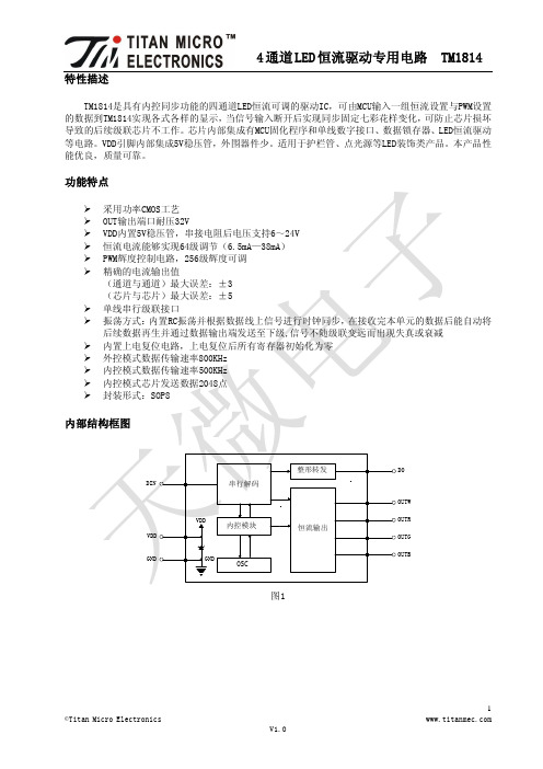
内部结构框图
VDD VDD
GND
GND
FIN
PWM控制 OSC
恒流 输出 驱动
●●● ●●●
OUT0 OUT15 FOUT
©Titan Micro Electronics
V1.3
1
16 通道 LED 流星雨恒流驱动 TM1928
管脚排列
VDD FIN OUT15 OUT14 OUT5 OUT4 OUT3 OUT2 OUT0 OUT1
AC220V输 入
R1 51 0K
VLED
C1
20 5 J /40 0V
10 3
LED LED
LED
LED LED
LED
LED LED
LED
1
2 3 4
5 6 7
8 9 10
VDD GND
FIN FOUT OUT15OUT13 OUT14OUT12
OUT5 OUT11 OUT4 OUT10 OUT3 OUT9
OUT2 OUT8 OUT0 OUT6 OUT1 OUT7
20
极限参数(1)(2)
参数名称
参数符号
极限值
单位
逻辑电源电压
VDD
-0.5~+7.0
V
输入端电压范围
FIN
Vfin
-0.5~VDD+0.5
V
输出32
mA
输出端电压范围
OUT0-OUT15
Vout
-0.5~+24.0
V
同步信号频率
FIN
Ffin
500
Hz
工作温度范围
100
单位
μF KΩ Ω μF
V KΩ
220V/50Hz交流电情况下,通常电容C1的容量C与总电流ILED的关系可近似认为:C=14.5×ILED。其 中,C的单位是μF,ILED的单位是A。当不同OUT端口间LED灯珠总压降不同时,例如虽然每个OUT端口都 并联2路、每路串联3个LED灯珠,但是部分端口串红色LED,部分端口串绿色LED,部分端口串蓝色LED, 则串红色LED的通道的灯珠总压降较低,此通道应串接适当的电阻,否则可能因阻容电路驱动不足而导 致花样显示异常。设OUT0-OUT15各通道灯珠总压降分别为V0-V15,Vmax为其中的最大值,则OUTn通道应 串接电阻的阻值计算公式为:
最小值
TM1928
典型值
800 1 450 900 50
最大值
单位
Hz s ms ms Hz
应用信息
1、交流供电模式
AC220V输入
R1 510K C1 205 J /400V
VLED
R4
LED
LED
LED LED
D1
D2
D3
D4
VDD 1 2 3 4 5 6 7 8 9 10
R2 51Ω/2W
VLED C2
©Titan Micro Electronics
V1.3
2
16 通道 LED 流星雨恒流驱动 TM1928
输入输出等效电路
VDD
VDD
OUTx
FIN
FOUT
GND
GND
GND
集成电路系静电敏感器件,在干燥季节或者干燥环境使用容易产生大量静电,静电放电可能 会损坏集成电路,天微电子建议采取一切适当的集成电路预防处理措施,不正当的操作和焊 接,可能会造成 ESD 损坏或者性能下降,芯片无法正常工作。
Topr
-40~+85
℃
储存温度范围
Tstg
-55~+150
℃
人体模式(HBM) 机器模式(MM)
ESD
2000
V
200
V
(1)芯片长时间工作在上述极限参数条件下,可能造成器件可靠性降低或永久性损坏,天微电子不建
议实际使用时任何一项参数达到或超过这些极限值;
(2)所有电压值均相对于系统地测试。
推荐工作条件
在 VDD=5.0V 及工作温度为-40℃~+85℃下测试,典型值在
VDD=5.0V 和 Ta=+25℃条件下得出,除非另有说明
参数名称
参数符号
测试条件
PWM 频率
Fout
FIN 悬空
花样周期时间 单通道开启时间 通道总开启时间 FOUT 输出频率
Tt T1 T2 Ffout
FIN 悬空 FIN 悬空 FIN 悬空 FIN 悬空
在-45℃~+85℃下测试,除非另有说明
参数名称
参数符号
测试条件
电源电压
VDD
VDD 到电源不串电阻
VDD 稳压管电流
ICC
正常工作电压下的电流
FIN 电压输入范围
Vfin
OUT 输出耐压范围
Vout
OUT=OFF
FOUT 脚输出频率
Ffout
FIN 悬空
FIN 脚输入频率
Ffin
工作温度范围
Ta
工作结温范围
9V
350Ω
12V
650Ω
24V
1.8KΩ
FIN通过采样电阻R4,直接采样220V交流市电用于芯片的同步信号输入。FIN内部设有电压钳位电路,
可以将FIN脚电压钳位在6V左右,FIN输入电流建议控制在2mA到5mA之间,建议采样电阻阻值在100K到50K
之间,选择的R4阻值越小,消耗的功率越大。
由于芯片OUT口恒流输出,需要在端口加一定的电压才能进入恒流区域。所以为了保证芯片OUT口工
典型值
2 510 51 220
104 103
100
外围元件参数配置—参考
最大值
备注
在一定交流电压下,提供的总电流取决于阻容电容
C1 的放电电阻
限流电阻,可省略
稳压电容
VDD 稳压电阻,依据供电 VDD 选择
芯片 VDD 稳压滤波电容,不可省
FIN 输入滤波电容,不可省
24
依据需要选择稳压值,注意稳压管的功率
R3=(VLED-VDD)/Idd。假设选择流经 VDD 的电流 Idd 为 10mA,稳压值 VDD 为 5.5V,则电源供电电压不同 情况下的 R3 电阻值如下表:
各电压下 R3 的参考阻值
电源电压 DC
建议电源接口与 VDD 间连接电阻 R3 值
5V
0Ω(无需接电阻,内部稳压管不工作)
6V
50Ω
作在恒流状态下,同时考虑到芯片功耗,OUT口加的电压应该保持在2V左右,且不能高于6V。当高于6V
时,应在灯珠上串接合适电阻,使OUT口电压保持在2V左右。
©Titan Micro Electronics
V1.3
5
16 通道 LED 流星雨恒流驱动 TM1928
3、应用实例 (1)每个驱动通道并联2路、每路串联3个蓝色LED灯珠,稳压管V1选用12V稳压值,则每个通道灯
1
20
2
19
3
18
4
17
5 Top View 16
6
15
7
14
8
13
9
12
10
11
GND FOUT OUT13 OUT12 OUT11 OUT10 OUT9 OUT8 OUT6 OUT7
管脚功能
管脚名称 管脚序号 I/O