顺络贴片电感选型手册
贴片电感DFE201610E-100M 品牌TOKO规格书推荐
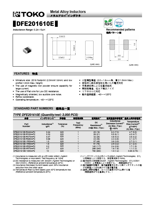
DFE201610EInductance Range: 0.24~10μH(Unit: mm)(Unit: mm)∙ Miniature size: 2016 footprint (2.0mm×1.6mm) and low profile(1.0mm Max. height)∙ The use of magnetic iron powder ensure capability for large current.∙ The use of Flat wire for Low DC resistance. ∙ Magnetically shielded, low audible core noise. ∙ Reflow solderable.∙ Operating temperature : -40~+125°C ∙ 小型薄型構造 (2.0x1.6mm角、高さ1.0mm Max.) ∙ 磁性材に鉄系磁性粉を用いた大電流対応 ∙ 平角線採用による低直流抵抗 ∙ 閉磁路構造、低コア鳴きノイズ ∙ リフロはんだ対応∙動作温度範囲:-40~+125°C(1) Inductance is measured with a LCR meter 4284A (Agilent Technologies ) or equivalent. Test frequency at 1MHz(2) DC resistance is measured with 34420A (Agilent Technologies) or 3541(HIOKI). (Reference ambient temperature 20°C)(3) Inductance Decrease Current based upon 30% inductance reduction from the initial value(4) Temperature Rise Current based upon 40°C temperature rise. (Reference ambient temperature 20°C)(1) インダクタンスはLCR メータ4284A (Agilent Technologies ) または同等品により測定する。
通用型贴片电容规格书(选型手册)

【 南京南山半导体有限公司 — 贴片电容选型资料】MULTILAYER CHIP CERAMIC CAPACITORCOG/COHCOG, ,-55125,030ppm/060ppm/0805CG101J500NT(PF) ( 0402 0.04 0603 0.06 0805 0.08 1206 0.12 ) 0.02 0.03 0.05 0.06 1.00 1.60 2.00 3.20 ( ) 0.50 0.80 1.25 1.60 CG CH COG NPO COH 100 101 102 10 100 1J G C B D5.00% 2.00% 0.25PF 0.10PF 0.50PF10 10 10 1026R3 100 250 5006.3V 10V 25V 50VS C N / / T BWBWTL mm L 0402 0603 0805 1206 1005 1608 2012 3216 1.00 1.60 2.00 3.20 0.05 0.10 0.20 0.30 W 0.50 0.80 1.25 1.60 0.05 0.50 0.10 0.80 0.20 0.80 1.00 1.25 0.20 0.80 1.00 1.25 T WB 0.05 0.25 0.10 0.30 0.20 0.50 0.20 0.20 0.20 0.60 0.20 0.20 0.10 0.10 0.20 0.3015【 南京南山半导体有限公司 — 贴片电容选型资料】0.80 0.20 1.00 0.20 0.50 0.80 0.20 1.00 0.20 0.600.20 0.30【 南京南山半导体有限公司 — 贴片电容选型资料】MULTILAYER CHIP CERAMIC CAPACITORCOG/COH 0402 0603 0805 12066.3V 10V 16V 25V 50V 6.3V 10V 16V 25V 50V 6.3V 10V 16V 25V 50V 6.3V 10V 16V 25V 50V0.5PF 1PF 2PF 3PF 4PF 5PF 6PF 7PF 10PF 22PF 33PF 47PF 68PF 100PF 120PF 150PF 180PF 220PF 330PF 470PF 560PF 680PF 1000PF 2200PF 2700PF 3300PF 4700PF 5600PF 6800PF 10nF 12nF 15nF 22nF 47nF 68nF 100nF17【 南京南山半导体有限公司 — 贴片电容选型资料】04020603080512066.3V 10V 16V 25V 50V 6.3V 10V 16V 25V 50V 6.3V 10V 16V 25V 50V 6.3V 10V 16V 25V 50VCapacitance0.5PF 1PF 2PF 3PF 4PF 5PF 6PF 7PF 10PF 22PF 33PF 47PF 68PF 100PF 120PF 150PF 180PF 220PF 330PF 470PF 560PF 680PF 1000PF 2200PF 2700PF 3300PF 4700PF 5600PF 6800PF 10nF 12nF 15nF 22nF 47nF 68nF 100nF【 南京南山半导体有限公司 — 贴片电容选型资料】MULTILAYER CHIP CERAMIC CAPACITORCOG COHPH~SLCOG PH SH SL TH RH UJCOH1-55125-55851. 2. 3. 2 4. 5. , , , , , 103 4 Cr 5PF 0.56% -4 5PF Cr 50PF 1.5 [(150/Cr)+7] 10 Cr 50PF 0.15% C C 10nF Ri 10nF Ri 5 10 Cr 500s 3 50mA 150+0/-10 8 25 9 75 235 5 2 0.5 25 60 265 10 1 25 : 1 2 100 170 120 200 1 1 2.5mm/ 24 2 5 5 5 2.5mm/ 245 24 -55 125 2 -55 85 60 510:HP4278A 1. 2. 3. (D.F.) :1.0 C : : (HP4284 25 5 0.2V 0.1MHz; 0.1KHZ ) 1000PF,1.0 :SF2511 , 60 60 1 5 :30% 75%5:C<1000PF,1.06I.R.7>3x150+0/-10 5% 0.5PF D.F. 10 I.R. 24 245【 南京南山半导体有限公司 — 贴片电容选型资料】General COGCOHPHSL MLCC reliability test methodStandard Number Item COG COH MLCC for General-use -55 125 PH, RH, SH, TH, UJ, SL MLCC for General-use -55 85 Check by using microscope 10 . Test Method1Operating Temperature RangeAppearance21.Good ceramic body color continuity. 2.The chips have no visual damages and must be very smooth. 3.No exposed inner- electrode, no cracks or holes. 4.The outer electrode should have no cracks, holes, damages or surface oxidation. 5.Outer electrode no prolongation or the prolongation is less than half of that of the termination width.3 4 5Dimensions Capacitance Dissipation Factor (DF)Within the specified dimensions Within the specified tolerance Cr 5PF 0.56% 5PF Cr 50PF 1.5 [(150/Cr)+7] 10-4 Cr 50PF 0.15% C C 10nF Ri 10nF Ri 5 1010 Cr 500sUsing micrometer or vernier calipers Measuring Equipments:HP4278 capacitance meter,HP4284 capacitance, Measuring Conditions: 1.Measuring Temperature:25 5 .Humidity: 30% 75%. 2.Measuring Voltage:1.0 0.2V. 3.Measuring Frequency:C<1000PF 1.0 0.1MHz C 1000PF 1.0 0.1KHz Measuring Equipment:Insulation resistance meter (such as Sf2511 insulation resistance). Measuring Method:Must measure at rated voltage, and measure the IR within 60 5 seconds. Must measure at 3 times rated voltage, dwell time: 60 1 seconds, no short and the changing/discharging current less than 50mA. First, pre-heat: heat treat 60 5 minutes at 150+0/-10 , then set it for 24 2 hours at room temperature. Measure the capacitance at -55 125 or -55 85 , the capacitance change ratio comparing to that of 25 must be within the specified range. Dip the capacitor into ethanol or colophony solution, and then dip it into 235 5 ( or 245 5 leadless eutedtic solder solution ) eutectic solder solution hanving lead for 2 0.5 seconds. Dipping speed: 25 2.5mm/second. First pre-heat: heat treat for 60 5 minutes at 150+0/-10 , then set it for 24 2 hours at room temperature. Then pre-heat the capacitance according to the following chart. Dip the capacitor into 265 5 eutectic solder solution for 10 1 seconds. Then set it for 24 2 hours at room temperature, then measure. Dipping speed: 25 2.5mm/second. Preheat conditions: Stage 1 2 Temperature 100 170 120 200 Time 1minute 1minute6Insulation Resistance7Withstanding Voltage Capacitance Temperature Characteristic>3x rated continuous working voltage Must meet the capacitor character temperature coefficient requirements within the operating temperature range. Tin coverage should be 75% of the outer electrode Appearance Cap. Change ratio DF No defects visible 5%or 0.5PF (whichever is larger)89SolderabilityResistance to Soldering10Same as original spec Same as original specIR46【 南京南山半导体有限公司 — 贴片电容选型资料】MULTILAYER CHIP CERAMIC CAPACITOR1 10N11 10N,10 1 :1.0mm/ 11.5mm 10 D.F. 12 55Hz 210 55Hz 10Hz 6 123 420 mm mmmm13mmmmmmmm150+0/-10 14 24 2 24 260 547【 南京南山半导体有限公司 — 贴片电容选型资料】NumberItems Adhesive Strength of TerminationStandard No removal of the terminations or other defect shall occurTest Method Solder the capacitor to the test jig (glass epoxy resin board) shown in Fig.1 using a eutectic solder.Then apply a 10N force inthe direction shown as the arrowhead.The aoldering shall be done either with an iron or using the reflow method and shall be conducted with care so that an iron or using the refow method and shall be conducted with care so that the soldering is uniform and free of defects such as heat shock,etc. 10N,10 1s Speed:1.0mm/s Glss epoxy resinboard11Fig.1 Vibration Resistance Appearance Capacitance No defects or abnormities Within the specified tolerance range Same as original spec12DFSolder the capacitor to the test jig (glass epoxy resin board). The capacitor should be subjected to a simple harmonic motion having a total amplitude of 1.5mm, the frequency being varied uniformly between the approximate limits of 10 and 55Hz, shall be traversed (from 10 Hz to 55 Hz then 10 Hz again) in approximately 1 minute.This motion shall be applied for a period of 2 hours in each 3 mutually perpendicular directions (total is 6 hours).Same i standarFif.2 Bending Resistance No cracks or other defects shall occur Solder the capacitor to the test jig (glass epoxy resin board) shown in Fig.3 using a eutectic solder. Then apply a 10N force in the direction shown as Fig.4. The soldering shall be done either with an iron or using the reflow method and shall be conducted with care so that the soldering is uniform and free of defects such as mm heat shock, etc.mm13mm mm mm14Temperature CycleAppearance No defects or abnormitiesPre-treatment: Heat-treat the capacitor for 60 5minutes at 150+0/-10 , then set it for 24 2 hours at room temperature. Perform five cycles according to the four heat treatments listed in the following table. Set it for 24 2 hours at room temperature, then measure.48mm【 南京南山半导体有限公司 — 贴片电容选型资料】MULTILAYER CHIP CERAMIC CAPACITOR2.5% 0.25PF, 1 10000M 2 3 4 2 3 30 3 2 3 30 3 2 314D.F. I.R.40 290 95 24 2500+24/-05% 0.5PF, 15 ( ) D.F. I.R. 10000M40 2 500+24/-0 5% 0.5PF, 16 D.F. I.R. 10000M90 95 24 22 50mA 5% 0.5PF, 17 D.F. I.R. 10000M1000 12 24 249【 南京南山半导体有限公司 — 贴片电容选型资料】NumberItem Temperature CycleStandard Cap. Change ratio D.F. I.R. 2.5% or 0.25 PF (whichever is larger) Same as original spec More than 10000M Heat-treatment:Test Method14stage temperature 1 lowest opeating temperature 3 2 normal temperature 3 high operating temperature 2 4 normal temperaturetime min. 30 3 2 3 30 3 2 3Humidity Steady StateAppearance Cap. Change ratio D.F. I.R.No defects or abnormities 5% or 0.5 PF (whichever is larger) Same as original spec More than 10000MSet the capacitor for 500+24/-0 hours at the condition of 40 2 and 90-95% humidity. Then remove and set it for 24 2 hours at room temperature, then measure.15Humidity LoadAppearance Cap. Change ratioNo defects or abnormities 5% or 0.5 PF (whichever is larger) Same as original spec More than 10000MApply rated voltage to the capacitor for 500+24/-0 hours at the condition of 40 2 and 90-95% humidity. Remove and set it for 24 2 hours at room temperature, then measure.16D.F. I.R.Life TestAppearance Cap. Change ratioNo defects or abnormities 5% or 0.5 PF (whichever is larger) Same as original spec More than 10000MApply two times rated voltage to the capacitor for 1000 12 hours at the upper temperature limits, the charging current should be less than 50mA. Remove and set it for 24 2 hours at room temperature, then measure.17D.F. I.R.5057-10%-5%0%5%10%COG 50VX7R 50V Z5U 50V Y5V50V010********-100%-80%-60%-40%-20%0%20%40%[Vdc]COG :1MHZ X7R,Z5U,Y5V:1KHZZ5U 50VY5V 50V X7R 50VC0G 50V0123-20%0%+20%+40%+60%^+80%COG PH RH SH TH UHCOG X7R Y5V,Z5U05010010001000010%0%-10%-20%-30%-40%[Hr]X7R20%0%[Vr ms ]COG :1MHZ X7R,Z5U,Y5V:1KHZMULTILAYER CHIP CERAMIC CAPACITOR58-5%0%5%10%-100%-80%-60%-40%-20%0%20%40%Z5U 50VY5V 50V X7R 50VC0G 50V0123-20%0%+20%+40%+60%^+80%COG X7R Y5V,Z5U05010010001000010%0%-10%-20%-30%-40%0%GENEREL-USE MLCC CHARCCTER PROFILESCapacitance change ratio DC Voltage[Vdc]Measuring condition COG :1MHzX7R,Z5U,Y5V:1KHzCOG and PHRH SH TH UH siriestemperature coefficentDC Capacitance-AC VoltageCharactericsCapacitance change_agingTime[Hr]X7R tempreture characteristicsZ5U [Vr ms ]Capacitance change ratioCapacitance change ratio Capacitance change ratio Capacitance change ratio。
顺络叠层电感规格书
顺络叠层电感规格书1. 引言顺络叠层电感作为电子电路中重要的元件之一,其规格书的编写就显得尤为重要。
本文将详细探讨顺络叠层电感规格书的编写要点和注意事项。
2. 规格书结构一个完整的顺络叠层电感规格书应包括以下几个部分:2.1 产品概述在产品概述部分,应对顺络叠层电感的基本特点进行简要介绍,包括其工作原理、主要用途、外形尺寸等。
2.2 技术指标在技术指标部分,应详细列出顺络叠层电感的各项基本参数,如电感值、额定电流、频率范围、温度特性等。
同时,还应注明测试方法和测量精度等详细要求。
2.3 结构形式结构形式部分应对顺络叠层电感的具体结构进行描述,包括内部材料、引线方式、外壳材料等。
2.4 生产工艺生产工艺部分应简要介绍顺络叠层电感的生产过程和关键工艺,如材料的选取、卷绕方式、烧结工艺等。
2.5 质量控制质量控制部分应详细描述顺络叠层电感在生产过程中的质量控制措施和标准,如检测方法、抽样方案、产品合格标准等。
2.6 包装和运输包装和运输部分应说明顺络叠层电感的包装方式,如采用卷盘或胶带包装,以及运输时的注意事项。
3. 规格书编写要点3.1 清晰明了编写规格书时,应使用简洁明了的语言,避免使用模糊不清或歧义的词汇。
规格书应能够清晰地传达产品的各项参数和特性。
3.2 准确无误规格书应准确地描述产品的各项指标,避免出现错误或误导性的信息。
在列举技术指标时,应注意标明测量单位和测量条件。
3.3 结构合理规格书的结构应合理,各个部分之间应有明确的逻辑关系,便于读者理解和查找信息。
可以利用标题、子标题和有序列表等方式来清晰地划分不同的章节和内容。
3.4 数据完备规格书中所列举的数据应完备,不应遗漏重要的参数和特性。
如果有多种型号或规格的产品,应分别列出其对应的数据。
3.5 数量一致规格书中列举的数据和参数应与实际产品一致,不应存在虚假宣传或与实际不符的情况。
对于有变动的参数,应及时更新规格书。
4. 总结顺络叠层电感规格书的编写是确保产品信息准确传递的重要工作。
顺络绕线电感规格书

※□: The inductance tolerance can be provided upon customer’s request. Please contact your local sales.
■2
顺络电子 Sunlord ■
规格特性
SDWL1005C-S TYPE
SPECIFICATIONS
■ 顺络电子 Sunlord
03■
规格特性
SDWL1005C-G TYPE
SPECIFICATIONS
Part Number 型号
Inductance 电感量
Min. Quality L/Q Test Max. DC
Tolerance
公差
Factor
Freq. Resistance
品质因子 测试频率 直流电阻
250
0.060
G, J, K
13
250
0.070
G, J, K
16
250
0.070
G, J, K
16
250
0.070
1360 1300 1040 1040 1040
12700 12000 11500 11300 11100
※□: The inductance tolerance can be provided upon customer’s request. Please contact your local sales.
Max. Rated Current 额定电流
mA Ir 570 570 460 430 370 400 330 330 320 320 260 250 250 240 200 200 190 190 170 140 140 140 130 130
技术大牛教你电感如何选型

技术⼤⽜教你电感如何选型器件选型是硬件⼯程师的基本⼯作,本⽂主要从电感的⼯艺和应⽤出发,介绍电感如何选型。
⼀、电感的基本原理电感,和电容、电阻⼀起,是电⼦学三⼤基本⽆源器件;电感的功能就是以磁场能的形式储存电能量。
以圆柱型线圈为例,简单介绍下电感的基本原理如上图所⽰,当恒定电流流过线圈时,根据右⼿螺旋定则,会形成⼀个图⽰⽅向的静磁场。
⽽电感中流过交变电流,产⽣的磁场就是交变磁场,变化的磁场产⽣电场,线圈上就有感应电动势,产⽣感应电流:电流变⼤时,磁场变强,磁场变化的⽅向与原磁场⽅向相同,根据左⼿螺旋定则,产⽣的感应电流与原电流⽅向相反,电感电流减⼩;电流变⼩时,磁场变弱,磁场变化的⽅向与原磁场⽅向相反,根据左⼿螺旋定则,产⽣的感应电流与原电流⽅向相同,电感电流变⼤。
以上就是楞次定律,最终效果就是电感会阻碍流过的电流产⽣变化,就是电感对交变电流呈⾼阻抗。
同样的电感,电流变化率越⾼,产⽣的感应电流越⼤,那么电感呈现的阻抗就越⾼;如果同样的电流变化率,不同的电感,如果产⽣的感应电流越⼤,那么电感呈现的阻抗就越⾼。
所以,电感的阻抗于两个因素有关:⼀是频率;⼆是电感的固有属性,也就电感的值,也称为电感。
根据理论推导,圆柱形线圈的电感公式如下:可以看出电感的⼤⼩与线圈的⼤⼩及内芯的材料有关。
实际电感的特性不仅仅有电感的作⽤,还有其他因素,如:· 绕制线圈的导线不是理想导体,存在⼀定的电阻;· 电感的磁芯存在⼀定的热损耗;· 电感内部的导体之间存在着分布电容。
因此,需要⽤⼀个较为复杂的模型来表⽰实际电感,常⽤的等效模型如下:等效模型形式可能不同,但要能体现损耗和分布电容。
根据等效模型,可以定义实际电感的两个重要参数。
⾃谐振频率(Self-Resonance Frequency)由于Cp的存在,与L⼀起构成了⼀个谐振电路,其谐振频率便是电感的⾃谐振频率。
在⾃谐振频率前,电感的阻抗随着频率增加⽽变⼤;在⾃谐振频率后,电感的阻抗随着频率增加⽽变⼩,就呈现容性。
顺络射频电感及参数简介

内容提要
顺络电子简介 电感的电性参数和分类 顺络电子的电感系列 射频电感的功能和应用注意事项 顺络新技术及射频电感发展趋势
公司概况
★战略目标:通过全球化的发展战略和科技创新,成为在全球被动电子 元器件及技术解决方案领域中具有技术领先和核心竞争优 势的国际化企业。
▲总资产: RMB13亿 ▲注册资本:RMB2.12亿 ▲性 质: 中港合资企业 ▲投资比例:中国55%/香港45% ▲员工人数:2373( 2013年9月30日止 )
片式电感
阻抗匹配 谐振滤波
扼流
电感的作用——阻抗匹配
Τ type network
Z1
Z3
ZC1
Z2
ZC2
ZC1 chg -1
Z1 =
ZC1ZC2 ?
ZC2 shg
Z2 =
ZC1ZC2 shg
Z3 = ZC1ZC2 ?
ZC 2 chg -1 ZC1
shg
Π type network
Z2
Z1
ZC1
Z3 ZC2
字母
B
C
电感量档位:
S
D
标准的电感量档位是通过字母来反映。
F
G
H
J
K
精度
±0.1nH ±0.2nH ±0.3nH ±0.5nH
±1% ±2% ±3% ±5% ±10%
电感的电性参数
Q (品质因子): 电感的Q值是电感相对损耗的一个度量,被称为“品质因子”。它的定义是电
感储能与耗能的比值,即电抗与有效电阻的比值,如下公式
补充说明:电信号选择阻抗低的通路传输。当频率低时,沿着导体的电感通 路阻抗更低(ZL=2πfL),所以器件在低频时呈现为电感的特性;频率高时, 从电极层间或电极与端电极之间的容性阻抗更低( ZC=1/2πfC ),因此器件
viking贴片磁珠电感CBM系列选型手册

Size (Inch) 0201 0402 0603 0805 1204 1210 1808 1812 2220 2220 2220
A
0.6±0.03 1.0±0.10 1.6±0.20 2.0±0.20 3.2±0.20 3.2±0.20 4.5±0.25 4.5±0.25 5.59±0.51 5.59±0.51 5.59±0.51
DCR (Ω) max.
0.05 0.20 0.20 0.40 0.40 0.40 0.45 0.50 0.20 0.60 0.65 0.70 0.28 0.35 0.75 0.45 0.75 0.90 1.00 1.10 1.00 1.50 0.80 0.58 0.49 0.80 0.80
Rated Current (mA) max. 500 300 300 200 200 200 200 200 500 200 100 100 700 300 100 400 100 100 100 50 300 50 250 300 350 250 250
H: High current G: Medium current N: General current F: High Frequency C: High current &
High Frequency
■Standard Electrical Specifications(for General Signal Line Use)
■ Applications
-Computers and Peripheral Equipment -VCRS, Television, Pagers -Cellular Phones -Digital Communication Equipment -Various Electronics Equipments -Circuit Where a Stable Ground is Unavailable
美国线艺Coilcraft汽车级贴片电感0603LS 系列选型规格书
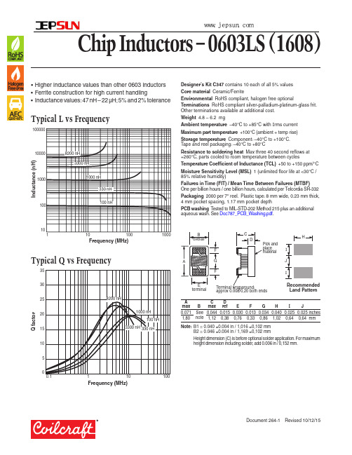
Chip Inductors – 0603LS (1608)• Higher inductance values than other 0603 inductors • Ferrite construction for high current handling• Inductance values: 47 nH – 22 µH; 5% and 2% toleranceI n d u c t a n c e (n H )10Frequency (MHz)Typical L vs FrequencyDesigner’s Kit C347 contains 10 each of all 5% values Core material Ceramic/FerriteEnvironmental RoHS compliant, halogen free optionalTerminations RoHS compliant silver-palladium-platinum-glass frit. Other terminations available at additional cost.Weight 4.8 – 6.2 mgAmbient temperature –40°C to +85°C with I rms current Maximum part temperature +100°C (ambient + temp rise)Storage temperature Component: –40°C to +100°C. Tape and reel packaging: –40°C to +80°CResistance to soldering heat Max three 40 second reflows at +260°C, parts cooled to room temperature between cyclesTemperature Coefficient of Inductance (TCL) +50 to +150 ppm/°C Moisture Sensitivity Level (MSL) 1 (unlimited floor life at <30°C / 85% relative humidity)Failures in Time (FIT) / Mean Time Between Failures (MTBF) One per billion hours / one billion hours, calculated per Telcordia SR-332Packaging 2000 per 7″ reel. Plastic tape: 8 mm wide, 0.23 mm thick, 4 mm pocket spacing, 1.17 mm pocket depthPCB washing T ested to MIL-STD-202 Method 215 plus an additional aqueous wash. See Doc787_PCB_Washing.pdf .Frequency (MHz)Q f a c t o rTypical Q vs Frequencyapprox 0.008/0,20 both endsterminalRecommended Land PatternNote: B1 = 0.040 ±0.004 in / 1,016 ±0,102 mmB2 = 0.046 ±0.004 in / 1,169 ±0,102 mmHeight dimension (C) is before optional solder application. For maximum height dimension including solder, add 0.006 in / 0,152 mm.A C D 深圳捷比信--高品质精密元件供应商www.jepsun.comChip Inductors – 0603LS SeriesInductance 2 Percent SRF min 4 DCR max 5 I rms 6Color OverallPart number 1 (nH) tolerance Q min 3 (MHz) (Ohms) (A)code width0603LS-47NX_L_ 47 @ 7.9 MHz 5,2 12 @ 7.9 MHz 1500 0.075 1.40 Black B10603LS-51NX_L_ 51 @ 7.9 MHz 5,2 12 @ 7.9 MHz 1400 0.075 1.00 Violet B10603LS-72NX_L_ 72 @ 7.9 MHz 5,2 12 @ 7.9 MHz 1400 0.12 1.40 Brown B10603LS-101X_L_ 100 @ 7.9 MHz 5,2 12 @ 7.9 MHz 1150 0.13 1.40 Red B10603LS-121X_L_ 120 @ 7.9 MHz 5,2 12 @ 7.9 MHz 1100 0.15 1.40 Orange B10603LS-151X_L_ 150 @ 7.9 MHz 5,2 15 @ 7.9 MHz 1050 0.15 1.30 Y ellow B10603LS-181X_L_ 180 @ 7.9 MHz 5,2 15 @ 7.9 MHz 950 0.15 1.30 G reen B10603LS-241X_L_ 240 @ 7.9 MHz 5,2 15 @ 7.9 MHz 800 0.16 0.95 Violet B10603LS-271X_L_ 270 @ 7.9 MHz 5,2 15 @ 7.9 MHz 775 0.30 0.71 G ray B10603LS-331X_L_ 330 @ 7.9 MHz 5,2 15 @ 7.9 MHz 725 0.46 0.56 White B10603LS-391X_L_ 390 @ 7.9 MHz 5,2 15 @ 7.9 MHz 620 0.51 0.50 Black B10603LS-471X_L_ 470 @ 7.9 MHz 5,2 15 @ 7.9 MHz 540 0.62 0.42 Brown B10603LS-561X_L_ 560 @ 7.9 MHz 5,2 15 @ 7.9 MHz 525 0.44 0.55 Red B10603LS-681X_L_ 680 @ 7.9 MHz 5,2 15 @ 7.9 MHz 260 0.52 0.47 Orange B20603LS-781X_L_ 780 @ 7.9 MHz 5,2 15 @ 7.9 MHz 460 0.83 0.39 Y ellow B10603LS-821X_L_ 820 @ 7.9 MHz 5,2 15 @ 7.9 MHz 410 0.69 0.40 G reen B10603LS-102X_L_ 1000 @ 7.9 MHz 5,2 15 @ 7.9 MHz 190 0.81 0.40 Blue B20603LS-122X_L_ 1200 @ 7.9 MHz 5,2 15 @ 7.9 MHz 160 0.87 0.37 Violet B2 0603LS-152X_L_ 1500 @ 7.9 MHz 5,2 15 @ 7.9 MHz 100 0.96 0.35 G ray B2 0603LS-182X_L_ 1800 @ 7.9 MHz 5,2 15 @ 7.9 MHz 80 1.1 0.35 White B2 0603LS-222X_L_ 2200 @ 7.9 MHz 5,2 15 @ 7.9 MHz 68 1.2 0.32 Black B2 0603LS-272X_L_ 2700 @ 7.9 MHz 5,2 15 @ 7.9 MHz 60 1.5 0.28 Brown B2 0603LS-332X_L_ 3300 @ 7.9 MHz 5,2 15 @ 7.9 MHz 42 1.5 0.28 Red B2 0603LS-392X_L_ 3900 @ 7.9 MHz 5,2 15 @ 7.9 MHz 40 1.6 0.28 Orange B2 0603LS-472X_L_ 4700 @ 7.9 MHz 5,2 15 @ 7.9 MHz 34 2.1 0.26 Y ellow B20603LS-562X_L_ 5600 @ 7.9 MHz 5,2 15 @ 7.9 MHz 32 2.6 0.24 G reen B20603LS-682X_L_ 6800 @ 7.9 MHz 5,2 15 @ 7.9 MHz 31 3.1 0.20 Black B20603LS-782X_L_ 7800 @ 7.9 MHz 5,2 15 @ 7.9 MHz 28 3.5 0.20 Blue B20603LS-822X_L_ 8200 @ 7.9 MHz 5,2 15 @ 7.9 MHz 26 3.6 0.19 Violet B20603LS-103X_L_ 10,000 @ 2.5 MHz 5,2 12 @ 2.5 MHz 25 4.8 0.18 G ray B20603LS-153X_L_ 15,000 @ 2.5 MHz 5,2 20 @ 2.5 MHz 23 7.1 0.17 White B20603LS-183X_L_ 18,000 @ 2.5 MHz 5,2 20 @ 2.5 MHz 22 7.6 0.16 Brown B20603LS-223X_L_ 22,000 @ 2.5 MHz 5,2 22 @ 2.5 MHz 19 8.81 0.13 Black B21. When ordering, specify tolerance, termination and packaging codes:0603LS-822X JLCTolerance: G = 2% J = 5% (T able shows stock tolerances in bold.)Termination: L = RoHS compliant silver-palladium-platinum-glass frit. E = Halogen free component. RoHS compliant silver-palladium-platinum-glass frit terminations.Special order: T = RoHS tin-silver-copper (95.5/4/0.5) or S = non-RoHS tin-lead (63/37).Packaging: C = 7″ machine-ready reel. EIA-481 embossed plastictape (2000 parts per full reel).B = Less than full reel. In tape, but not machine ready.To have a leader and trailer added ($25 charge), use code letter C instead.2. Inductance measured at 0.1 V rms, using Coilcraft SMD-A fixture in Agilent/HP 4286A impedance analyzer with Coilcraft-provided correlation pieces.3. Q measured on Agilent/HP 4395A with Agilent/HP 16193 test fixture.4. SRF measured using Agilent/HP 8753D network analyzer with Coilcraft SMD-D test fixture.5. DCR measured on Cambridge T echnology Micro-ohmmeter.6. Current that causes a 15°C temperature rise from 25°C ambient. Because of their open construction, these parts will not saturate. T his information is for reference only and does not represent absolute maximum ratings7. Electrical specifications at 25°C.Refer to Doc 362 “Soldering Surface Mount Components” before soldering.深圳捷比信--高品质精密元件供应商www.jepsun.com。
- 1、下载文档前请自行甄别文档内容的完整性,平台不提供额外的编辑、内容补充、找答案等附加服务。
- 2、"仅部分预览"的文档,不可在线预览部分如存在完整性等问题,可反馈申请退款(可完整预览的文档不适用该条件!)。
- 3、如文档侵犯您的权益,请联系客服反馈,我们会尽快为您处理(人工客服工作时间:9:00-18:30)。
绕线贴片功率电感—ASWPA 系列
Wire Wound SMD Power Inductors – ASWPA Series
Operating temperature range: -40℃~+125℃ (Including self-heating)
特征 FEATURES
● 磁性胶水涂敷结构极大减少了蜂鸣声
● 直接在磁芯上金属化电极,抗跌落冲击强,经 久耐用
● 闭合磁路结构设计,漏磁少,抗EMI 能力强
● 同等尺寸,额定电流特性较传统电感高出30% 以上
● AEC-Q200D 认证
用途 APPLICATIONS
● 车载信息娱乐系统 ● LED 灯 ● 安全气囊
● 除汽车电源系统以外的DC-DC 转换器
产品型号 PRODUCT IDENTIFICATION
ASWPA 4035 S 1R0 N T □□□
① ② ③ ④ ⑤ ⑥ ⑦
● Magnetic-resin shielded construction reduces buzz noise to ultra-low levels
● Metallization on ferrite core results in excellent shock resistance and damage-free durability ● Closed magnetic circuit design reduces leakage flux and Electro Magnetic Interference (EMI) ● 30% higher current rating than conventional inductors of equal size ● AEC-Q200D verified
● Infotainment system ● LED Lighting ● Airbag
● DC-DC conversion except for vehicle power
外观尺寸 SHAPE AND DIMENSIONS
Fig.1 Fig.2
规格特性 SPECIFICATIONS
Note: ※ 1: Rated current: Isat (max.) or Irms (max.), whichever is smaller;
※ 2: Saturation Current: Max. Value, DC current at which the inductance drops less than 20% from its value without current; Typ. Value, DC current at which the inductance drops 30% from its value without current;
※ 3: Heat Rating Current: DC current that causes the temperature rise (ΔT) from 20°C ambient. For Max. Value, ΔT<40℃; For Typ. Value, ΔT is approximate 40℃.
The part temperature (ambient + temp. rise) should not exceed 125 °C under worst case operating conditions. Circuit design, component placement, PCB trace size and thickness, airflow and other cooling provisions all affect the part temperature. Part temperature should be verified in the end application。