声子晶体
椭圆柱三维简立方排列声子晶体的带隙结构
椭圆柱三维简立方排列声子晶体的带隙结构
椭圆柱三维简立方排列声子晶体,是基于声子晶体衍射加工技术而发
展起来的新型光功能材料。
它具有众多独特的性质,如光学耦合效应,低损耗衍射散射,卓越的可塑性和独立性等。
当然,最重要的是它的
带隙结构。
1、带隙结构
椭圆柱三维简立方排列声子晶体的带隙结构是它的主要特征,简单地说,带隙就是由重复出现的长度元件组成的排列状况,从而形成与其
他相关材料不同的电磁场的分布。
也就是说,椭圆柱三维简立方排列
声子晶体的带隙结构吸纳更多的光子,并表现出差分布的电磁场特性
模式,使椭圆柱三维简立方排列声子晶体具有更佳的独立性能以及光
学耦合效应。
2、低损耗衍射散射
椭圆柱三维简立方排列声子晶体具有突出的特性,例如低损耗衍射散射。
其带隙结构可以有效地减少散射信号传播子件之间的耦合,从而
使散射信号保持清晰且不呈现失真,同时降低损耗。
3、卓越的可塑性
椭圆柱三维简立方排列声子晶体具有卓越的可塑性,它可以通过精密
的带隙排列形式和复杂的衍射结构,来实现集中的控制性能的优化。
这些控制性能可以进一步扩展,使它具有更丰富的功能性能,从而满足应用需求。
4、独立性
椭圆柱三维简立方排列声子晶体具有出色的独立性,这是由于其低损耗衍射散射效果和可塑性来实现的。
利用独立性特性,可以在光学领域生产各种精确的设计。
总的来说,椭圆柱三维简立方排列声子晶体的带隙结构具有一系列独特的性能,如低损耗衍射散射,卓越的可塑性和独立性,使其成为当今光功能材料中的重要材料,广泛应用于光学,电子等方面。
声子晶体中的拓扑声学:探索声子晶体中的拓扑相与声波调控

声子晶体中的拓扑声学:探索声子晶体中的拓扑相与声波调控摘要拓扑声学是凝聚态物理学和声学交叉领域的新兴方向,研究声子晶体中的拓扑相及其对声波传播的调控。
本文深入探讨了拓扑声学的概念、原理、实验进展及其潜在应用。
通过对声子晶体中拓扑绝缘体、拓扑半金属、拓扑角态等拓扑相的介绍,阐述了拓扑声学在声波操控、新型声学器件设计等方面的独特优势。
引言拓扑声学(Topological Acoustics)是近年来兴起的跨学科领域,将拓扑物理的概念引入声学系统,研究声子晶体中受拓扑保护的声波传播现象。
声子晶体(Phononic Crystals)是由不同材料周期性排列而成的人工结构,其能带结构中存在带隙,可以禁止特定频率范围的声波传播。
拓扑声学通过引入拓扑不变量来描述声子晶体的能带结构,发现了许多受拓扑保护的声学现象,如拓扑绝缘体、拓扑半金属、拓扑角态等。
这些拓扑相具有独特的声波传播特性,为声波操控和新型声学器件设计提供了新的思路。
拓扑声学的原理拓扑声学的核心概念是拓扑不变量。
拓扑不变量是描述系统整体性质的物理量,不随系统的连续形变而改变。
在拓扑声学中,拓扑不变量可以用来表征声子晶体的能带结构。
当声子晶体的拓扑不变量发生变化时,其能带结构也会发生突变,出现新的拓扑相。
拓扑声学中的拓扑相主要包括:1. 拓扑绝缘体:拓扑绝缘体在体内是绝缘体,但在边界或界面上存在受拓扑保护的导电态。
拓扑声学绝缘体在体带隙中禁止声波传播,但在边界上存在受拓扑保护的声表面波或声边缘态。
这些拓扑态具有单向传播、背散射抑制等特性,可用于设计新型声波导、声隔离器等。
2. 拓扑半金属:拓扑半金属在能带结构中存在能带交叉点,称为Weyl点或Dirac点。
拓扑声学半金属具有类似的能带交叉点,其附近的声子具有线性色散关系。
拓扑声学半金属中的声波传播具有手性反常、负折射等特性,可用于设计新型声学透镜、声学天线等。
3. 拓扑角态:拓扑角态是存在于拓扑绝缘体拐角处的一种受拓扑保护的局域态。
一维声子晶体

一维声子晶体一维声子晶体是指在一维结构中存在声子的空间周期性排列现象。
声子是晶体中的一种元激发,表现为晶格中原子或离子的振动。
一维声子晶体的研究有助于我们更好地理解声子的传播和控制声波的性质。
一维声子晶体的形成是通过周期性重复的单元结构,其中每个单元都包含了相同的声子离散能级。
这种周期性结构可以由交错排列的不同材料的多层薄膜构成,也可以是周期性重复的晶格结构。
在一维结构中,声子的传播受到晶格的限制,只能在特定的频率范围内传播。
一维声子晶体的研究主要集中在声子的禁带特性和声子局域化效应。
禁带是指在一维结构中存在某些频率范围内声子无法传播的区域。
这种禁带的形成是由于周期性结构的干涉效应导致的。
当声子频率位于禁带内时,声子会被禁止传播,从而发生局域化现象。
这种局域化现象在一维声子晶体中可以被用来控制和调控声波的传播。
一维声子晶体在声学器件中有着广泛的应用。
通过调控一维声子晶体的结构参数,比如周期、层数和材料的选择等,可以实现声波的频率选择性传播和滤波功能。
这在声学通信、声学传感和声学隔离等领域具有重要的应用价值。
此外,一维声子晶体还可以用于研究声子的量子效应和拓扑性质,为声子学的进一步发展提供了重要的实验平台。
除了一维声子晶体,还存在二维和三维声子晶体。
二维声子晶体是指在二维结构中存在声子的周期性排列现象,三维声子晶体则是指在三维结构中存在声子的周期性排列现象。
二维和三维声子晶体的研究也具有重要的科学意义和应用价值,可以用于实现更复杂的声学器件和研究更多样化的声子行为。
一维声子晶体作为声学材料的一种特殊形态,具有独特的声子传播特性和应用潜力。
通过对一维声子晶体的研究,可以深入理解声子的行为和声波的传播规律,为声学器件的设计和应用提供新的思路和方法。
随着声子学的进一步发展,一维声子晶体的研究将在更多领域展示出其重要性和应用前景。
声子晶体带结构研究
第二章,基于弹性波波动方程,介绍了计算声子晶体带结构最常用的 方法——平面波展开法,简述研究二维和三维声子晶体的理论模型。
第三章,计算了二维固态-固态声子晶体中不同散射体按正方形排列 时的带结构,计算结果表明:(1)当散射体的填充率取不同值时,频率最 低的带隙的最大值所对应的散射体截面形状不同;(2)当散射体的截面为 长方形时, 截面的长宽比为 1.2 时 XY 模的带隙最宽,长宽比为 1 时 Z 模 的带隙最宽;(3)当散射体横截面是正方形并旋转角 θ 时,当 θ=45o时 最有利于带隙的产生。
In chapter 2, based on the elastic wave equation, we introduce the traditional method for the calculation of band structure, namely the method of plane wave expansion. In addition, theoretic models to study 2D and 3D phononic crystals are presented.
Finally, a summary of our works and outlook for future works on the investigation of phononic crystals are presented in chapter 5.
Key words: Phononic crystals; Energy band structure; Phononic band gaps; Plane wave expansion method.
声子——精选推荐

声子晶体概述XXX院(系):理学院专业:应用化学学号:********** 指导教师:韩喜江2013年3月题目声子晶体专业应用化学学号*********X 学生XXX指导教师韩喜江摘要声子晶体就是弹性常数在空间呈周期性排列的人工晶体。
声子晶体是由弹性固体周期排列在另一种固体或流体介质中形成的一种新型功能材料。
通过类比光子晶体,人们发现弹性波在周期弹性复合介质中传播时,也会产生类似于光子带隙的弹性波带隙,从而提出了声子晶体的概念。
由于声子晶体具有禁带、缺陷态等特性使得它在减振、降噪、声学器件等方面有着潜在的应用前景。
关键词:声子;声子晶体;减振;降噪。
一、声子概念的提出◆1883年,Floquet关于一维Mathieus方程的研究,首次考虑了周期结构中波的传播。
◆1887年,Rayleigh率先研究了连续周期结构中波的传播特性,指出结构中存在无波传播的频带。
◆1953年,Brillouin对波在周期介质中的传播特性进行了系统深入的研究。
◆1992年,M.MSigalas,E.N.Econnmou首次从理论上证实了三维周期点阵结构中弹性波带隙的存在性。
◆1993年,M.S.Kushwaha研究二维周期介质时首次明确提出声子晶体的概念。
◆2000年9月,Science刊登了刘正猷提出的声子晶体的局域共振带隙机理。
二、声子晶体的特性由于声子晶体具有弹性波带隙,它具有这样的性质:、减缓波速效应、声聚焦、弹性波定向、超准直、沿缺陷传播、声吸收、等效的负刚度、负密度、负折射率、和光子的相互作用、声致热导率减小、反常多普勒效应等特性。
因此声子晶体多用于减振、降噪、声学器件方面。
声子晶体和我们平时接触的晶体是不一样的,声子晶体是多种弹性介电材料组成的周期性结构,研究对象是弹性波在晶体中的传播,波动是一种弹性波(电磁波),声子晶体的晶格是0.1到1um,它的特征是弹性波(光子)带隙和缺陷表面态;而平时我们接触的晶体多为电子晶体,是一种结晶体,其研究对象是其电子的运输行为,波动为德布罗意波,晶格为0.1到0.5nm,其特征是电子带隙、缺陷态和表面态。
声子晶体六角晶格

声子晶体六角晶格
声子晶体,又称为弹性波晶体或声波晶体,是一种具有周期性结构的人工复合材料,其内部结构设计用于调控弹性波(包括声波)的传播。
六角晶格声子晶体是声子晶体的一种常见结构,其晶格排列类似于蜂窝状结构,具有较高的对称性和空间效率。
六角晶格声子晶体的独特之处在于其能带结构,这种结构可以影响声波在其中传播的方式。
通过精确控制材料的组成、形状和排列,研究人员可以设计出声波带隙,即在特定频率范围内阻止声波传播的区域。
这种特性使得六角晶格声子晶体在隔音、振动控制和声波聚焦等领域具有广泛的应用前景。
在六角晶格声子晶体中,声波的传播受到晶格周期性结构的影响,类似于电子在晶体中的行为。
当声波的频率与晶体的某个固有频率相接近时,声波的传播会受到强烈的散射和反射,从而导致声波的传播受到阻碍。
这种散射和反射的效果可以通过调整晶格的大小、形状和材料的属性来进一步控制。
除了基本的隔音功能外,六角晶格声子晶体还可以用于设计高效的声波聚焦器件。
通过精确控制晶格的结构和参数,研究人员可以创造出能够将声波聚焦到特定点的器件,这对于声波成像、声波通信和声波操控等领域具有重要意义。
总的来说,六角晶格声子晶体是一种具有独特结构和功能的人工材料,其在声波调控和操控方面展现出巨大的潜力。
随着研究的深入和技术的不断发展,六角晶格声子晶体有望在未来的声波科技领域发挥更加重要的作用。
21世纪最具潜力的新型带隙材料_声子晶体_塔金星
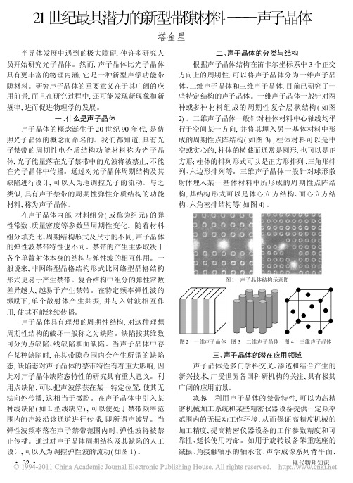
21世纪最具潜力的新型带隙材料 声子晶体塔金星半导体发展中遇到的极大障碍,使许多研究人员开始研究光子晶体。
然而,声子晶体比光子晶体具有更丰富的物理内涵,它是一种新型声学功能带隙材料。
研究声子晶体的重要意义在于其广阔的应用前景,而且在研究过程中,还可能发现新现象和新规律,进而促进物理学的发展。
一、什么是声子晶体声子晶体的概念诞生于20世纪90年代,是仿照光子晶体的概念而命名的。
我们都知道,具有光子禁带的周期性电介质结构功能材料称为光子晶体,光子能量落在光子禁带中的光波将被禁止,不能在光子晶体中传播。
通过对光子晶体周期结构及其缺陷进行设计,可以人为地调控光子的流动。
与之类似,具有声子禁带的周期性弹性介质结构的功能材料,称为声子晶体。
在声子晶体内部,材料组分(或称为组元)的弹性常数、质量密度等参数呈周期性变化。
随着材料组分填充比、周期结构形式及尺寸的不同,声子晶体的弹性波禁带特性也不同。
禁带的产生主要取决于各个单散射体本身的结构与弹性波的相互作用。
一般说来,非网络型晶格结构形式比网络型晶格结构形式更易于产生禁带。
复合结构中组分的弹性常数差异越大,越易于产生禁带。
在特定频率弹性波的激励下,单个散射体产生共振,并与入射波相互作用,使其不能继续传播。
声子晶体具有理想的周期性结构,对这种理想周期性结构的破坏一般称之为缺陷。
缺陷按其维数可分为点缺陷、线缺陷和面缺陷。
当声子晶体中存在某种缺陷时,在其带隙范围内会产生所谓的缺陷态,缺陷态对声子晶体的禁带特性有着重大影响,因此对声子晶体缺陷态特性的研究具有重大意义。
利用点缺陷,可以把声波俘获在某一特定位置,使其无法向外传播,这相当于微腔。
在声子晶体中引入某种线缺陷(如L型线缺陷),可以使处于禁带频率范围内的声波沿该通道进行传播,即所谓声波导。
当弹性波频率落在声子禁带范围内时,弹性波将被禁止传播。
通过对声子晶体周期结构及其缺陷的人工设计,可以人为调控弹性波的流动(如图1)。
声子晶体研究概述_温激鸿

随后 , 人们发现当弹性波在周期性弹性复合介质中 传播时 , 也会产生类 似的弹性波 禁带 , 于是提 出了声 子晶体概 念 。 声子 晶体具有丰富的物理内涵及潜在的广阔应用前景 。 声子晶体的 研究引起了各国研究机构的高度关注[ 6 ~ 39] 。
表 1 3 类晶体波带结构特性比较 T able 1 Band-structure-related properties of three crystals
(电子)晶体
光子晶体
声子晶体
属性
由 两 种(或 以 上) 由两种(或以上)
结晶体
介 电 材 料构 成 的 弹性材料构成的
(自然的或生长的)
功能材料
1992 年 , M .M .Sigalas 和 E.N .Economou 第 1 次 在理 论上 证实球形散射体埋入某一基体材料中形成三维周期性点阵结构 具有弹性波 禁带特性[ 6] 。 1993 年 , M .S .Kushw aha 等人第 1 次 明确提出了声子晶体(P hononic Cry stals)概念 , 并 对镍柱 在铝合 金基体中形成的复合介质采用平面波方法计算获得了在剪切极 化方向上的弹性波禁带[ 7] 。 1995 年 , R .M artinez-Sala 等人在对 西班牙马德里的一座 200 多年前制作的雕塑“流动的旋律” 进行 声学特性研 究 时 , 第 1 次从 实 验角 度 证 实了 弹 性波 禁 带 的存 在[ 12] 。 从此声子晶体的研究引起了极大关注 。
- 1、下载文档前请自行甄别文档内容的完整性,平台不提供额外的编辑、内容补充、找答案等附加服务。
- 2、"仅部分预览"的文档,不可在线预览部分如存在完整性等问题,可反馈申请退款(可完整预览的文档不适用该条件!)。
- 3、如文档侵犯您的权益,请联系客服反馈,我们会尽快为您处理(人工客服工作时间:9:00-18:30)。
Waveguiding in two-dimensional piezoelectric phononic crystal platesJ. O. Vasseur, A.-C. Hladky-Hennion, B. Djafari-Rouhani, F. Duval, B. Dubus, Y. Pennec, and P. A. DeymierCitation: Journal of Applied Physics 101, 114904 (2007); doi: 10.1063/1.2740352View online: /10.1063/1.2740352View Table of Contents: /content/aip/journal/jap/101/11?ver=pdfcovPublished by the AIP PublishingArticles you may be interested inVibration band gaps in double-vibrator pillared phononic crystal plateJ. Appl. Phys. 119, 014903 (2016); 10.1063/1.4939484Acoustic beam splitting in two-dimensional phononic crystals using self-collimation effectJ. Appl. Phys. 118, 144903 (2015); 10.1063/1.4932138Surface acoustic wave band gaps in a diamond-based two-dimensional locally resonant phononic crystal for high frequency applicationsJ. Appl. Phys. 111, 014504 (2012); 10.1063/1.3673874Propagation of acoustic waves and waveguiding in a two-dimensional locally resonant phononic crystal plate Appl. Phys. Lett. 97, 193503 (2010); 10.1063/1.3513218Lamb waves in plates covered by a two-dimensional phononic filmAppl. Phys. Lett. 90, 021909 (2007); 10.1063/1.2431569Waveguiding in two-dimensional piezoelectric phononic crystal plates J.O.Vasseur,a͒A.-C.Hladky-Hennion,B.Djafari-Rouhani,F.Duval,B.Dubus,andY.PennecInstitut d’Electronique,de Micro-électronique et de Nanotechnologie,UMR CNRS8520,CitéScientifique,59652Villeneuve d’Ascq Cedex,FranceP.A.DeymierDepartment of Materials Science and Engineering,University of Arizona,Tucson,Arizona85721͑Received27February2007;accepted12April2007;published online5June2007͒We investigate the possibility of designing phononic crystal-based devices for telecommunicationapplications using materials commonly employed in microfabrication.We focus our attention on aphononic crystal made of a square array of cylindrical holes drilled in an active piezoelectric PZT5Amatrix.Two different structures are considered,namely,a freestanding phononic crystal plate and aplate deposited on a silicon substrate.The geometrical characteristics of the phononic crystal plates͑lattice parameter and thickness͒were chosen to ensure the existence of an absolute band gap around1.5GHz;a common frequency in radio frequency putations of thedispersion curves of these active structures were conducted with the help of thefinite elementmethod.We demonstrate the existence of absolute band gaps in the band structure of the phononiccrystal plates and,then,the possibility of guided modes inside a linear defect created by removingone row of air holes in the phononic crystal.In the case of the supported phononic crystal plates,weshow the existence of an absolute forbidden band in the plate modes when the thickness of thesubstrate significantly exceeds the plate thickness.We discuss the conditions to realize waveguidingthrough a linear defect inside the supported plate.The present work provides evidences thatphononic crystal properties can be integrated with existing silicon based microdevice technology.©2007American Institute of Physics.͓DOI:10.1063/1.2740352͔I.INTRODUCTIONThe propagation of elastic waves in periodic composite media,such as phononic crystals,has been the object of many researchers’interest in the past decade.1–3Phononic crystals are created by a two-dimensional or three-dimensional periodic arrangement of inclusions in a matrix. Phononic crystals may exhibit absolute band gaps where the propagation of elastic waves is forbidden in all directions. These band gaps arise under certain conditions of contrast in density and elastic properties,composition,geometry of the array of inclusions,and inclusion shape.When the periodic-ity of a phononic crystal is broken,it is possible to create highly localized defects within the acoustic bang gap,which are analogous to localized modes in photonic crystals and to localized impurity states in semiconductors.Extended de-fects such as rows of different inclusions in the phononic lattice have been shown to guide elastic waves within the crystal band gap.Defect modes can then lead to functional-ities such asfiltering and multiplexing.4–8In addition to bulk phononic crystals,e.g.,composite media of infinite extent along the three spatial directions, semi-infinite phononic crystals with a free surface have been shown to support surface acoustic waves͑SAWs͒.The peri-odicity of the crystal in the plane of the surface may open gaps in the SAW branches.For instance,the existence of SAW localized at the free surface of a semi-infinite two-dimensional phononic crystal has been proven theoretically.9–12For this geometry,the parallel inclusions are of cylindrical shape and the considered surface is perpen-dicular to their axis.Various arrays of inclusions,9,10crystal-lographic symmetries of the component materials,11and also the piezoelectricity of one of the constituents12were taken into account.On the experimental side,Wu et al.13observed high frequency SAW with a pair of interdigitated transducers placed on both sides of a thick silicon plate in which a square array of holes was drilled.Similar experiments were con-ducted by Benchabane et al.on a two-dimensional square lattice piezoelectric phononic crystal etched in lithium niobate.14These studies suggest that integration of phononic crystals with radio frequency SAW devices may lead to a significant enhancement of the telecommunication device’s functionality.Slabs of phononic crystals also possess the characteristic properties of their bulk and semi-infinite counterparts.Gaps form in the symmetric Lamb mode band structure of two-dimensional phononic crystal plates composed of triangular arrays of W cylinders in a Si background.15Zhang et al.16 have shown the existence of gaps for acoustic waves propa-gating in an air/aluminium two-dimensional͑2D͒phononic crystal plate through laser ultrasonic measurements.Absolute band gaps appear in the band structure of phononic crystal plate composed of passive17,18or piezoelectric materials.19 The existence of these absolute gaps depends strongly on the ratio of the plate thickness to the crystal periodicity with the largest gap occurring when this ratio is around1.To obtaina͒Author to whom correspondence should be addressed;electronic mail:jerome.vasseur@univ-lille1.frJOURNAL OF APPLIED PHYSICS101,114904͑2007͒0021-8979/2007/101͑11͒/114904/6/$23.00©2007American Institute of Physics101,114904-1gaps at telecommunication frequencies of the order of giga-hertz,the thickness of the plate should be of the order of micrometers.On the other hand,the realization of telecom-munication devices requires,in general,the phononic crystal plates to be supported by a substrate.In this paper,we report on the properties of piezoelectric phononic crystal freestanding plates and a plate supported on a silicon substrate.We focus on acoustic wave propagation in these structures and unravel the conditions under which ab-solute band gaps form for the plate modes.We also consider freestanding and supported phononic crystal plates contain-ing rectilinear defects and we demonstrate the ability of the defect to guide acoustic waves with frequencies falling in-side the forbidden band of the parent phononic crystal plate.The paper is organized as follows.In Sec.II,we present the models of bulk phononic crystals,of phononic crystal plates,and of plates deposited on a substrate together with thefinite element method used for calculating their band structures.In Sec.III,we discuss the behavior of the band structures with respect to the geometrical and physical pa-rameters.Finally,some conclusions are drawn concerning the applicability of these structures to functional telecommu-nication devices.II.MODELS AND METHOD OF CALCULATION The basic phononic crystal used throughout this paper is composed of a square array of parallel cylindrical air inclu-sions͑holes͒of radius R drilled in a PZT5A piezoelectric matrix.The cylindrical air inclusions are assumed parallel to the z axis of the Cartesian coordinates system͑O,x,y,z͒. Thefilling factorof inclusions is defined as=R2/a2 and taken to be0.7to ensure the existence of an absolute band gap in the band structure of the bulk phononic crystal.17 We choose the lattice parameter a of the periodic array equal to0.77m in order to locate the band gap around1.5GHz, a common frequency in telecommunications.The phononic crystal plates are cut perpendicular to the z axis.The thick-ness of the plate is denoted by h.Optimal conditions for gap formation in the plate modes are obtained for h of the same order as a.17In the case of supported plates,the substrate is constituted by silicon,an ubiquitous material in microdevice manufacturing.In the numerical calculations,silicon was as-sumed of cubic crystallographic symmetry.The thickness of the substrate is variable and defined as d͑see Fig.1͒.The physical characteristics of PZT5A and Si are reported in Tables I and II.The band structures were computed using thefinite ele-ment method.20According to the Bloch-Floquet relations,21 only the mesh of one unit cell is required.Dispersion curves of the bulk phononic crystal were calculated using a three-dimensional͑3D͒unit cell:the structure is supposed to be infinite and uniform along the z direction,infinite but peri-odic in the two other directions x and y.This structure is named a3D structure and,following the Bloch-Floquet theo-rem,a phase relation is applied on the six faces of the mesh. For the two other structures͑plate,plate deposited onto a substrate͒,a3D mesh is considered too but the structure is supposed to be offinite size along the thickness of the plate, periodic and infinite in the two other directions.Thus,it is named a2D periodic structure and a phase relation is applied on only four faces of the mesh.The unit cell is meshed and divided into elements connected by nodes.Within this cell,a phase relation is applied on nodes separated by one period, defining boundary conditions between adjacent cells.The phase relation is related to the wave number of the incident wave in the periodic material.In this study,isoparametric elements are used,with20nodes for each element͑hexahe-dron with one node at each corner and one node at the TABLE I.Physical characteristics of PZT5A:is the density,͑s E͒is the constant electricfield elastic tensor,͑d͒is the piezoelectric tensor,and͑S͒is the constant strain dielectric permittivity tensor.PZT5A is a hexagonal crystal,with6mm class symmetry.Constant Unit Valuekg/m37750s11E m2/N 1.640ϫ10−11s12E−5.740ϫ10−12s13E−7.220ϫ10−12s33E 1.880ϫ10−11s44E 4.750ϫ10−11d31C/N−1.710ϫ10−10d33 3.740ϫ10−10d15 5.840ϫ10−1011S1036033S9390FIG.1.͑a͒Freestanding phononic crystal plate of thickness h and͑b͒phononic crystal plate of thickness h deposited onto a homogeneous sub-strate of thickness d.The basic phononic crystal is composed of a squarearray of parallel cylindrical air inclusions͑holes͒of radius R drilled in apiezoelectric matrix.The lattice parameter is a.The cylindrical air inclu-sions are assumed parallel to the z axis of the Cartesian coordinates system͑O,x,y,z͒.TABLE II.Physical characteristics of silicon:is the density,C11,C12,andC44are the three independent elastic moduli of cubic silicon.Constant Unit Valuekg/m32331C11N/m216.57ϫ1010C12 6.39ϫ1010C447.962ϫ1010middle of each edge ͒,and a quadratic interpolation along element sides is considered,thanks to the three nodes per edge of the element.The band structures are rendered in terms of a frequency,function of the modulus of the wave vector,and are plotted along the principal directions of propagation of the 2D irreducible Brillouin zone ͑⌫XM ͒.III.RESULTS AND DISCUSSIONA.Freestanding PZT/air phononic crystal plate 1.Bulk phononic crystal and phononic crystal plateFigure 2͑a ͒gives the band structure of the infinite phononic crystal,where only propagation perpendicular to the cylinders is taken into account.One can notice the exis-tence of a band gap in the frequency range from 1.0596to 1.4460GHz.However,the band gap will be to-tally filled when taking into account the out-of-plane propa-gation.On the contrary,we have shown recently 17that a slab of a phononic crystal can display an absolute band gap pro-vided its thickness h is of the order of the in-plane lattice parameter a .This comes from the confinement of the modes in the slab that imposes limitations on the allowed values of the wave vector along the z axis.Figure 2͑b ͒gives the dis-persion curves of such a slab when h =a ;it shows an absoluteband gap ranging from 1.1808to 1.3072GHz.The three lowest branches in the band structure,starting at the ⌫point,are quite similar to those of a homogeneous slab.They,re-spectively,correspond to the antisymmetric A 0Lamb mode,the shear horizontal mode,and the symmetric S 0Lamb mode.2.Waveguide in the freestanding plateWe consider now the case of a rectilinear waveguide created inside the lead zirconate titanate ͑PZT ͒/air phononic crystal plate.A supercell containing seven unit cells in the y direction is considered in the finite element calculations.The lattice parameter a and the thickness of the plate h are the same as for the perfect plate.Two systems are investigated.In the first system,the seven unit cells contain an air hole.In the second system,the hole in the fourth unit cell is filled with PZT5A,thus constituting a linear waveguide in the x direction.Figures 3͑a ͒and 3͑b ͒show the band structure of the phononic crystal plate and the plate with a waveguide,respectively.We limit ourselves to the ⌫X path of the Bril-louin zone that corresponds to the direction of propagation of the elastic waves inside the waveguide.Figure 3͑a ͒exhibitsFIG.2.Elastic band structures calculated with the finite element method for ͑a ͒the bulk 2D phononic crystal ͑structure of infinite extent along the three spatial directions ͒and ͑b ͒the freestanding phononic crystal plate of thick-ness h =a =0.77m made of a square array of holes drilled in a PZT 5A piezoelectric matrix with =0.7.The inset represents the first Brillouin zone ͑⌫XM ͒of the square array.The components of the wave vector at the ⌫,M ,and M points are ͑0,0͒,͑/a ,0͒,and ͑/a ,/a ͒,respectively,with /a =4.08m −1.FIG.3.Band structure along the ⌫X direction calculated with a supercell containing 1ϫ7unit cell,for ͑a ͒the perfect phononic crystal plate and ͑b ͒the phononic crystal plate containing a waveguide formed by filling the hole in the fourth unit cell.The inset depicts the 1ϫ7supercell considered in each case.The two straight lines indicate the location of the guided mode analyzed in Fig.4.numerous additional branches with respect to those in Fig.2͑a ͒as the result of the folding of the bands in the y direction due to the seven unit-cell periodicity in that direction.The band structure still shows the same forbidden band as the one displayed in Fig.2͑b ͒.When a waveguide is introduced in the structure,guiding modes appear inside the band gap of the perfect phononic crystal plate,as illustrated in Fig.3͑b ͒.More specifically,we illustrate in Fig.4,the modulus of the displacement field for the waveguide mode having a fre-quency f =1.221GHz and a wave vector equal to 3.468m −1.Figure 4corresponds to a top view and a three-quarter view of the three-dimensional displacement field in the xy plane.It clearly shows that the acoustic displacement is concentrated within and in the close vicinity of the wave-guide.The displacement field is very weak in the rest of the phononic crystal since the mode considered lies within the forbidden band of the phononic crystal plate.B.PZT/air phononic crystal plate on a silicon substrate1.Perfect phononic crystal plate on silicon substrateIn the previous section,we considered a freestanding phononic crystal plate made of a square array of holes drilled in a PZT5A matrix.The geometrical characteristics of the plate,i.e.,the thickness h ,the lattice parameter a ,and the radius of the holes R were of the order of micrometers and were chosen in the aim of observing an absolute band gap around a frequency of 1.5GHz.A micrometer thick plate cannot be used effectively in device structures.The physical realization of a practical structure would then require that the thin plate of phononic crystal be deposited onto a thick sub-strate for support.In consequence,we investigate here the influence of a substrate on the absolute band gap of thephononic crystal plate.We consider a substrate of finite thickness d made of silicon.Figure 5shows the finite ele-ment band structure of the plate deposited on the substrate for d =2h =2a .The thick solid straight lines represent the dispersion curves of the slower elastic waves propagating in an infinite,homogeneous medium composed of silicon,i.e.,the waves of transverse polarization.One first observes that the substrate vibrational modes strongly interact with those of the phononic crystal plate,leading to very different dis-persion curves with respect to those of a freestanding plate ͓see Fig.2͑b ͔͒.Moreover,only modes below the dispersion curves of the transverse waves in silicon are confined inside the phononic crystal plate.With this restriction,the band structure of Fig.5appears to exhibit forbidden bands,in particular,along the XM direction of propagation.In the other directions of the Brillouin zone,the plate modes cross-over in the vicinity of the C t line of the substrate around 1.5GHz,for example,and appear below the C t line.In Fig.6,we present the same band structure but for a thicker sub-strate,i.e.,for d =5h =5a .In that case,one observes that,in the same range of frequency,some plate modes still appear below the C t line of the substrate but occur very closely to this line.This results in the existence of an absolute forbid-den band centered around f =1.5GHz.Our finiteelementFIG.4.͑Color online ͒Maps of the modulus of the elastic displacement field for the waveguide mode with f =1.221GHz and a wave vector of modulus 3.468m −1;͑a ͒top view and ͑b ͒three-quarter view.The red color corre-sponds to the maximum displacement,whereas the blue color corresponds to theminimum.FIG.5.Elastic band structures for the air/PZT phononic crystal plate of thickness h =a deposited onto a silicon substrate of thickness d =2h =2a .The thick solid lines represent the dispersion curves of the slower elastic waves propagating in an infinite,homogeneous medium composed of sili-con,i.e.,the waves of transversepolarization.FIG.6.Same as Fig.5but for a substrate thickness d =5h =5a .method ͑FEM ͒results also show that for much thicker sub-strate,the dispersion curves below C t remains the same.Our study shows also that the existence of such an absolute for-bidden band requires very constraining conditions on the na-ture of the materials constituting the phononic crystal and the substrate.2.Waveguide in the plate deposited on a silicon substrateWe investigate now the propagation of elastic waves through a rectilinear waveguide created inside the phononic crystal plate deposited on the silicon substrate.The rectilin-ear waveguide is created as in Sec.III A 2,and the finite element calculations are conducted in the same way.Never-theless,in that case the computations were done considering a 1ϫ5supercell.This allows one to reduce the computation time but does not affect significantly the numerical results.The band structures are calculated along the ⌫X path of the irreducible Brillouin zone ͓Fig.7͑b ͔͒.As a matter of com-parison,we present also in Fig.7͑a ͒the band structure of the perfect plate deposited on the substrate computed with a 1ϫ5supercell.The thickness of the plate and of the substrate are h =a and d =5h =5a ,respectively.Figure 7͑b ͒shows that some new modes occur in the forbidden band of Fig.7͑a ͒.To show the confinement of such modes inside the waveguide,we focus our attention on the mode with frequency f =1.4657GHz at the X point of the Brillouin zone ͓indicated by an arrow in Fig.7͑b ͔͒.The modulus of the displacement field associated with this mode is displayed on the map of Fig.8.This map unequivocally shows the localized nature of this mode indicating that it corresponds to a guided mode of the plate.The three-dimensional representation of the dis-placement field demonstrates that this guided mode is con-fined in the plate and does not leak out into the substrate.IV.CONCLUSIONSThe purpose of this paper was to investigate the possi-bility of designing phononic crystal-based devices for tele-communication applications using commonly employed ma-terials in microfabrication.We focused our attention on active piezoelectric PZT5A material and silicon.We demon-strated that absolute band gaps for the propagation of plate modes exist in PZT/air hole phononic crystal plates.Inciden-tally,we also show that plate modes can be guided inside a linear defect created by removing one row of holes.How-ever,practical devices would require that the phononic crys-tal plate be supported by a substrate.We therefore calculated the band structure of a PZT/air phononic crystal plate on a silicon substrate.Absolute forbidden band in the plate modes forms when the substrate thickness exceeds significantly that of the plate.This gap includes the ubiquitous telecommuni-cation frequency of 1.5GHz.We prove also that a linear defect in such a structure can guide plate mode.The present work provides evidences that phononic crystal properties can be integrated with existing silicon based microdevice tech-nology.This study also suggests that other structural defects such as point defects,cavities,and various channels inserted inside the phononic crystal plate could also lead to the exis-tence of vibrational modes inside the absolute stop bands.These defect modes could then be used to realize functional acoustic devices such as specific filters or demultiplexers.ACKNOWLEDGMENTSThis work was supported by Le Fond Européen de Développement Régional ͑FEDER ͒and by Le Conseil Ré-gional Nord—Pas de Calais.We acknowledge the assistance of M.Deymier with some of the graphic arts.We also thank P.Mosbah ͑ISEN,Lille ͒for his help with the finite element numerical computations.1J.O.Vasseur,B.Djafari-Rouhani,L.Dobrzynski,and P.A.Deymier,J.Phys.:Condens.Matter 9,7327͑1997͒.2D.García-Pablos,M.Sigalas,F.R.Montero de Espinosa,M.Torres,M.Kafesaki,and N.García,Phys.Rev.Lett.84,4349͑2000͒.3S.Yang,J.H.Page,Z.Liu,M.L.Cowan,C.T.Chan,and P.Sheng,Phys.Rev.Lett.93,024301͑2004͒.4Y .Pennec, B.Djafari-Rouhani,J.O.Vasseur, A.Khelif,and P. A.Deymier,Phys.Rev.E 69,046608͑2004͒.FIG.7.Band structure along the ⌫X direction calculated with a supercell containing 1ϫ5unit cell,for ͑a ͒the perfect phononic crystal plate deposited on the silicon substrate and ͑b ͒the supported plate containing a waveguide formed by filling a hole in the third unit cell.The thickness of the substrate is the same as in Fig.6,i.e.,d =5h =5a .The arrow indicates the location of the guided mode analyzed in Figs.8͑a ͒and 8͑b ͒.FIG.8.͑Color online ͒Maps of the modulus of the elastic displacement field for the waveguide mode with f =1.4657GHz at the X point in Fig.7͑b ͒;͑a ͒top view and ͑b ͒three-quarter view.The red color corresponds to the maxi-mum displacement,whereas the blue color corresponds to the minimum.5Y.Pennec,B.Djafari-Rouhani,J.O.Vasseur,rabi,A.Khelif,A. Choujaa,S.Benchebane,and ude,Appl.Phys.Lett.87,261912͑2005͒.6A.Khelif,A.Choujaa,S.Benchabane,B.Djafari-Rouhani,and ude, Z.Kristallogr.220,836͑2005͒.7T.Miyashita and C.Inoue,Jpn.J.Appl.Phys.,Part140,3488͑2001͒. 8T.Miyashita,Meas.Sci.Technol.16,R47͑2005͒.9Y.Tanaka and S.Tamura,Phys.Rev.B58,7958͑1998͒.10Y.Tanaka and S.Tamura,Phys.Rev.B60,13294͑1999͒.11T.T.Wu,Z.G.Huang,and S.Lin,Phys.Rev.B69,094301͑2004͒.ude,M.Wilm,S.Benchabane,and A.Khelif,Phys.Rev.E71, 036607͑2005͒.13T.T.Wu,Z.G.Huang,and S.Y.Liu,Z.Kristallogr.220,841͑2005͒;T. T.Wu,L.C.Wu,and Z.G.Huang,J.Appl.Phys.97,094916͑2005͒. 14S.Benchabane,A.Khelif,J.-Y.Rauch,L.Robert,and ude,Phys. Rev.E73,065601͑2006͒.15J.J.Chen,B.Qin,and J.C.Cheng,Chin.Phys.Lett.22,1706͑2005͒. 16X.Zhang,T.Jackson,fond,P.Deymier,and J.O.Vasseur,Appl. Phys.Lett.88,041911͑2006͒.17J.O.Vasseur,P.A.Deymier,B.Djafari-Rouhani,and Y.Pennec,Proceed-ings of IMECE2006,ASME International Mechanical Engineering Con-gress and Exposition,Chicago,Illinois,5–10,November2006.18J.C.Hsu and T.T.Wu,Phys.Rev.B74,144303͑2006͒.19A.Khelif,B.Aoubiza,S.Mohammadi,A.Adibi,and ude,Phys. Rev.E74,046610͑2006͒.20The band structures were computed with the help of the ATILAfinite ele-ment code,ATILA Finite Element Code for Piezoelectric and Magnetostric-tive Transducers Modeling,Version5.2.1,User’s Manual,ISEN,Acous-tics Laboratory,Lille,France͑2002͒.nglet,A.-C.Hladky-Hennion,and J.-N.Decarpigny,J.Acoust.Soc. Am.98,2792͑1995͒.。