基于LPC2478的触摸屏设计
如何用自带AD实现触摸屏转换(触摸屏)(AD转换)
LIU_XF (原创)如何用自带AD实现触摸屏转换(触摸屏)(AD转换)摘要:在人机界面中,触摸屏越来越流行,一般情况下,都需要一个触摸屏控制器或者触摸屏接口芯片来实现触摸屏的AD转换,但对于某些单片机系统,它并不带有触摸屏控制器,也不想增加外扩触摸屏芯片的成本,则可以用自带的AD来实现触摸屏的转换。
本文将以LPC2478平台介绍如何利用自带AD实现触摸屏AD转换及滤波的处理。
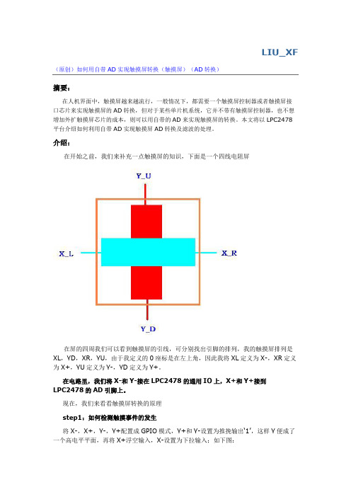
介绍:在开始之前,我们来补充一点触摸屏的知识,下面是一个四线电阻屏在屏的四周我们可以看到触摸屏的引线,可分别找出引脚的排列,我的触摸屏排列是XL,YD,XR,YU,由于我定义的0座标是在左上角,因此我将XL定义为X-,XR定义为X+,YU定义为Y-,YD定义为Y+。
在电路里,我们将X-和Y-接在LPC2478的通用IO上,X+和Y+接到LPC2478的AD引脚上。
现在,我们来看看触摸屏转换的原理step1:如何检测触摸事件的发生将X-,X+,Y-,Y+配置成GPIO模式,Y+和Y-设置为推挽输出‘1’,这样Y便成了一个高电平平面,再将X+浮空输入,X-设置为下拉输入;如下图:由于触摸屏的电阻是远小于R1(LPC2478自带下拉电阻)的,因此当触摸屏X Y有接触时,X-端会产生一个高电平,因此触摸事件的发生,就是通过检测这个高电平而得知的。
当然触摸屏按下和松开会有抖动,需要进行滤波处理,原理很简单,这里就不介绍了,看附件里的代码吧。
step2:检测X的值触摸事件发生后,我们要开始进行AD转换了,首先我们确定X的座标值。
将X+ X-设置为推挽输出,X+输出‘1’,X-输出‘0’,Y-设置为FLOAT输入,Y+设置为AD输入这样,AD转换出来的就是X的值。
当然,AD转换也是要滤波的,我采用的是中值滤波法,大家还是看代码吧。
step3:检测Y的值同step2一样的方法,可检测出Y的值。
step4:AD转换为键值/******************************************************************** 函数功能:触摸屏键值转换入口参数:返回:备注:********************************************************************/ void TouchScrConvert(TOUCH_SCR_STATUS *p_status){Int32U x_pixels;Int32U y_pixels;Int8U f_x=0,f_y=0;//无效值,直接返回==//如果超过范围==//xif(p_status->TouchScrX<=TOUCH_SCR_MIN_X_ADC){p_status->TouchScrX = 0; f_x=1;}elseif(p_status->TouchScrX>=TOUCH_SCR_MAX_X_ADC){p_status->TouchScrX = TOUCH_SCR_H_SIZE;f_x=1;}//yif(p_status->TouchScrY<=TOUCH_SCR_MIN_Y_ADC){p_status->TouchScrY = 0; f_y=1;}elseif(p_status->TouchScrY>=TOUCH_SCR_MAX_Y_ADC){p_status->TouchScrY = TOUCH_SCR_V_SIZE; f_y=1;}//--//--x_pixels = p_status->TouchScrX;y_pixels = p_status->TouchScrY;if(f_x==0){x_pixels = (x_pixels - TOUCH_SCR_MIN_X_ADC)*TOUCH_SCR_H_SIZE;x_pixels /= TOUCH_SCR_DELTA_X_ADC;}if(f_y==0){y_pixels = (y_pixels - TOUCH_SCR_MIN_Y_ADC) * TOUCH_SCR_V_SIZE; y_pixels /= TOUCH_SCR_DELTA_Y_ADC;}p_status->TouchScrX = (Int16U)x_pixels;p_status->TouchScrY = (Int16U)y_pixels;}关于触摸屏压力的检测其实,对于触摸屏来说等效电路应该是这样Rt是接触电阻,由于它是与R3串联接入AD的,因此它可以被忽略,但这个Rt 并非是无用,对于检测触摸压力还是有用的,因为对于有些PDA快速手写需要辩别触摸的压力,用下面的方法则可以实现结语:用自带AD,省去了外扩触摸屏芯片,节省了成本,也缩小了PCB面积。
LPC2478
1.一般说明恩智浦LPC2478微控制器的半导体设计,由供电的ARM7TDMI - S内核,是一个范围广泛的高度集成的微控制器应用程序需要先进的通讯和高质量的图形显示。
该LPC2478微控制器有512片上高速快闪存储器。
这闪光内存包括一个特殊的128位宽度的存储器接口和加速器架构,使CPU能够从闪存执行顺序指令时最高72 MHz的系统时钟速度。
此功能仅适用于ARM公司的LPC2000 微控制器系列产品。
与实时调试接口LPC2478,即包括JTAG和嵌入式跟踪,可以同时执行32位ARM和16位Thumb 指示。
在LPC2478微控制器集成了一个LCD控制器,一个10/100以太网媒体访问控制器(MAC),一个USB全速设备/主机/ OTG控制器,4 kB 的端点内存,4个UART,两个控制器局域网(CAN)通道,一个SPI 接口,两个同步(SSP)的串行端口,3个I2C接口,和一个I2S 接口。
支持这一接口的串行通信收集有以下特点部件;一个片4 MHz内部振荡器,98 KB的组成共64 KB的内存当地的SRAM,16个以太网,16个一般用途的DMA,2 KB的SRAM 的KB的SRAM的对KB电池供电的SRAM,一个外部存储器控制器(EMC)的。
这些特性使得本装置适用于便携式电子产品优化和点式销售终端(POS)应用程序。
补充了许多串行通信控制器,多功能计时功能,和记忆的功能是多方面的32位定时器,一个10位ADC,10位DAC,两个PWM单元,以及多达160快速GPIO线路。
在LPC2478的GPIO引脚连接到64 基于硬件的向量中断控制器(VIC)完成,这意味着这些外部输入可产生边沿触发中断。
所有这些特性使得LPC2478设备特别适用于工业控制和医疗系统等。
2.特点的ARM7TDMI - S处理器,运行速度高达72兆赫。
512 KB的片上闪存程序存储器的在系统编程(ISP)和在应用中编程(IAP)功能。
基于LPC2478的三相电力监测仪

关键 词 智 能 电 网 ;三 相 电 力 监 测 仪 :
L C 4 8; S1 7 P 2 7 AD 8 1
中 图 分 类 号 T 36 P0 文献 标 志 码 A
图 1 监 测 仪 网 络 拓 扑 结 构
收 稿 日期 2 1 42 0 1 -0 作 者 简 介 茅 文 铭 , , 士 , 要 从 事 称 重 测 试 仪 器 男 硕 主 仪表以及智能 电网方面的研究与开发工作.
CL K
P M0 W
行 接 口和 P WM 等 , 还带 有外部 总 线接 口、 S 20全 UB.
系列 接 口、 A L N接 口 、4位 的彩 屏 L D控 制 器 以及 2 C
片上 R C A S 1 8是 T 公 司 的 8通 道 1 T . D 17 I 6位 的 同
图 3 A S 1 8与 L C 4 8的 接 口 D 17 P27
能 达 到 国标 A 级 .
种 功 能更 加 强 大 , 作更 加 稳定 , 工 测量 精 度更 高 , 讯 实 时性 更 好 , 通
监测 仪在 实 际运 用 中的 网络拓 扑结 构 如 图 1 所示 .
使用 更加 简单 和便 捷 , 成本 更 加低 廉 的新 型 电力 监测 仪 .
文章编号 :6 47 7 ( 0 1 0 - 5 -4 17 .00 2 1 ) 50 20 4
基 于 L C 4 8的三 相 电 力 监测 仪 P 27
茅文铭 王恒斌 陈军
摘 要 介 绍 了 国 家 智 能 电 网 需 求 的 一 款 新
0 引言
三相 电力 监 测 仪 在 实 际工 业 用 电 中 发 挥 着 巨 大 作 用 . 随着 国家 智能 电网战略的推进 以及微 电子技术 和信 息技术 的发展 , 市场需求
LPC2478远程温度监控
随着通讯技术、网络技术和半导体技术的飞速发展,嵌入式系统接入网络已成为其应用的一个重要方向。
越来越多的嵌入式系统选择Web 服务器的方式与Internet 进行数据交换。
而以太网是构筑现代Internet 网络的基础,因此选择基于以太网的嵌入式Web 服务器技术实现数据交换将具有较高的实用价值。
温度是程控机房、档案室、图书馆、农业生产基地等众多场所需要实时监控的一个重要物理量。
温度监控系统在实际生活中有着重要的作用。
本文主要针对ARM7TDMI核的微处理器芯片,结合嵌入式Web 服务器技术,提出了基于以太网的远程温度监控系统的设计方案。
该方案成功的实现了温度采集和控制的网络化。
本设计采用的是丰宝公司的LINPO-PS LPC_2478实验板,进行远程温度监控系统研究,该板采用了恩智浦公司基于ARM7TDMI-S内核、单电源供电、LQFP208封装的LPC2478,具有JTAG仿真调试,ISP编程等功能。
uClinux是应用于微控制领域的一种嵌入式Linux操作系统,它源码开放,移植性好,支持多种硬件平台和几乎所有常见网络通信协议,支持文件系统丰富,是一个功能完整的嵌入式操作系统。
并且有大量优秀的开放源代码的应用软件和开发工具可用,因此,采用μClinux作为操作平台,使用Web技术进行远程在线监测系统的开发。
Boa是一个高性能的单任务型Web服务器,可以运行在几乎所有的类Unix的平台上,Boa支持认证,支持CGI,功能比较全,占用资源也少,非常适合于用在资源有限的嵌入式系统中,目前Boa已经以源码的形式包含在uClinux的发行包中。
所以本设计采用uClinux和boa服务器可以较好的满足本次设计要求。
关键词:远程温度系统;AMR7;LPC2478;u-boot;uClinux;nand flash;nor flash;dp83848;ds18b20;cgi;boa;web;Along with communications technology, networking technology and the technology embedded systems developing rapidly and access network has become an important direction of its application. more and more options embedded systems and internet web server exchange data.. And ethernet is construct a modern internet network infrastructure and therefore opt for ethernet technology embedded web server for data interchange will be the practical value of the room. the temperature is controlled, and the archives, libraries, agricultural production base in many places such as real-time monitoring require a major physical quantities. the temperature control system in practical life is an important role. This article mainly aimed at the microprocessor chips arm7tdmi, the technology embedded web server, based on the temperature of the ethernet remote control system design scheme. This scheme successful to the collection and control of the network.The design is based on the Fengbao Electronic Technology (Shanghai) Co., Ltd LINPO-PS LPC_2478 board to carry out the analysis on meter reading system, the board is integrated with NXP ARM7TDMI-S kernel, Single power supply, LQFP208 enclosed LPC2478, JTAG simulated debugging and ISP programming functions, etc.. This design adopts uclinux and the boa server can better meet the requirements.uClinux is applied to a control an embedded linux operating system of its open source and transplant well, and support multiple hardware platforms and almost all common communication protocols network, supported file system, is a function of embedded system. and there is a good open source software application and development of tools available, and therefore, adopt μ clinux as operating platform, the use of remote web technology in the monitoring system development.Boa is a performance of the task type of web server and run on almost all the kind of unix platforms, boa support and support, and the cgi be holding resources are few and are suitable for use in the limited resources of embedded systems, and the boa has been a source of the forms contained in the issue of uClinux package.So this design adopts uclinux and the boa server can better meet the requirements.Key words: remote temperature measurement and control system;ARM7;LPC2478;u-boot;uClinux;nand flash;norflash;dp83848;ds18b20;cgi;boa;web;目录引言 (5)1 项目设计方案 (6)2 开发环境介绍 (7)2.1LINPO-PS LPC_2478介绍 (7)2.2NORFLASH介绍 (7)2.2.1 AM29LV160DB简介 (8)2.2.2 AM29LV160DB的操作命令字 (8)2.2.3 Nor flash的映射 (8)2.3N AND FLASH介绍 (9)2.3.1 Nand flash芯片工作原理 (9)2.3.2 Nand flash主要内设命令详细介绍 (10)2.4以太网接口介绍 (11)2.4.1 以太网模块特点 (11)2.4.2 以太网模块初始化 (12)2.5软件开发环境的介绍 (13)3 U-BOOT的移植 (14)3.1U-B OOT简介 (14)3.1.1 LPC2468OEM_Board中几个重要的文件 (16)3.1.2 U-Boot的启动流程 (17)3.2U-B OOT的配置和编译 (19)3.3U-B OOT的移植 (19)3.4U-B OOT N OR FLASH驱动的移植 (21)3.5NAND F LASH 驱动移植 (23)3.6U-B OOT网卡驱动移植 (26)4 UCLINUX系统的移植 (30)4.1基本内核的移植 (30)4.2L INUX NOR FLASH驱动移植 (32)4.2.1 Linux mtd简介 (32)4.2.2 Nor flash驱动移植 (33)4.2.3 JFFS2文件系统的制作 (37)4.3L INUX网卡驱动移植 (38)4.3.1 网卡初始化 (39)4.3.2 网卡打开 (40)4.3.3 网卡发送 (40)4.3.4网卡接收 (40)4.3.5 网卡关闭 (41)4.3.6 网卡退出 (41)4.3.7 LPC2468网卡驱动移植 (41)4.4嵌入式W EB服务器BOA的移植 (43)4.4.1 Boa简介 (43)4.4.2 Boa编译配置 (43)4.4.3 Boa目录的建立 (44)4.4.4 Boa的编译 (44)5 软件开发过程 (45)5.1DS18B20驱动程序设计 (45)5.1.2 DS18B20硬件连接 (47)5.1.3 DS18B20驱动介绍 (47)5.1.4 温度应用程序 (49)5.2LPC2478DA驱动设计 (51)5.2.1 LPC2478 DA驱动测试 (51)5.3WEB程序设计 (51)5.3.1 CGI简介 (51)5.3.2 CGI程序工作原理 (52)5.3.3 WEB程序框图 (52)5.3.4 WEB程序介绍 (53)6 结论 (54)谢辞 (55)参考文献 (56)引言我国是粮食生产大国,同时我国地域辽阔,气候差异大,粮食的安全存储是一项重要任务。
LPC2478FET208资料
1.General descriptionNXP Semiconductors designed the LPC2478 microcontroller, powered by the ARM7TDMI-S core, to be a highly integrated microcontroller for a wide range ofapplications that require advanced communications and high quality graphic displays. The LPC2478 microcontroller has 512kB of on-chip high-speed flash memory. This flash memory includes a special 128-bit wide memory interface and accelerator architecture that enables the CPU to execute sequential instructions from flash memory at themaximum 72MHz system clock rate. This feature is available only on the LPC2000 ARM microcontroller family of products. The LPC2478, with real-time debug interfaces that include both JTAG and embedded trace, can execute both 32-bit ARM and 16-bit Thumb instructions.The LPC2478 microcontroller incorporates an LCD controller, a 10/100 Ethernet Media Access Controller (MAC), a USB full-speed Device/Host/OTG Controller with 4kB of endpoint RAM, four UARTs, two Controller Area Network (CAN) channels, an SPIinterface, two Synchronous Serial Ports (SSP), three I 2C interfaces, and an I 2S interface. Supporting this collection of serial communications interfaces are the following feature components; an on-chip 4MHz internal oscillator, 98kB of total RAM consisting of 64kB of local SRAM, 16kB SRAM for Ethernet, 16kB SRAM for general purpose DMA, 2kB of battery powered SRAM, and an External Memory Controller (EMC). These features make this device optimally suited for portable electronics and Point-of-Sale (POS) applications. Complementing the many serial communication controllers, versatile clocking capabilities,and memory features are various 32-bit timers, a 10-bit ADC, 10-bit DAC, two PWM units, and up to 160 fast GPIO lines. The LPC2478 connects 64 of the GPIO pins to thehardware based Vector Interrupt Controller (VIC) that means these external inputs can generate edge-triggered interrupts. All of these features make the LPC2478 device particularly suitable for industrial control and medical systems.2.FeaturesARM7TDMI-S processor, running at up to 72MHz.512kB on-chip flash program memory with In-System Programming (ISP) andIn-Application Programming (IAP) capabilities. Flash program memory is on the ARM local bus for high performance CPU access. 98kB on-chip SRAM includes:64kB of SRAM on the ARM local bus for high performance CPU access.16kB SRAM for Ethernet interface. Can also be used as general purpose SRAM. 16kB SRAM for general purpose DMA use also accessible by the USB. 2kB SRAM data storage powered from the RTC power domain.LPC2478Single-chip 16-bit/32-bit micro; 512 kB flash, ethernet, CAN, LCD, USB 2.0 device/host/OTG, external memory interfaceRev. 01 — 6 July 2007Preliminary data sheetFast communication chip LCD controller, supporting both Super-Twisted Nematic (STN) and Thin-FilmTransistors (TFT) displays.Dedicated DMA controller.Selectable display resolution (up to 1024×768 pixels).Supports up to 24-bit true-color mode.Dual Advanced High-performance Bus (AHB) system allows simultaneous Ethernet DMA, USB DMA, and program execution from on-chip flash with no contention.EMC provides support for asynchronous static memory devices such as RAM, ROM and flash, as well as dynamic memories such as Single Data Rate SDRAM.Advanced Vectored Interrupt Controller (VIC), supporting up to 32 vectored interrupts. General Purpose AHB DMA controller (GPDMA) that can be used with the SSP, I2S, and SD/MM interface as well as for memory-to-memory transfers.Serial Interfaces:Ethernet MAC with MII/RMII interface and associated DMA controller. These functions reside on an independent AHB bus.USB 2.0 full-speed dual-port device/host/OTG controller with on-chip PHY and associated DMA controller.Four UARTs with fractional baud rate generation, one with modem control I/O, one with IrDA support, all with FIFO.CAN controller with two channels.SPI controller.Two SSP controllers, with FIFO and multi-protocol capabilities. One is an alternate for the SPI port, sharing its interrupt. SSPs can be used with the GPDMA controller.Three I2C-bus interfaces (one with open-drain and two with standard port pins).I2S (Inter-IC Sound) interface for digital audio input or output. It can be used with the GPDMA.Other peripherals:SD/MMC memory card interface.160 General purpose I/O pins with configurable pull-up/down resistors.10-bit ADC with input multiplexing among 8 pins.10-bit DAC.Four general purpose timers/counters with 8 capture inputs and 10 compare outputs. Each timer block has an external count input.Two PWM/timer blocks with support for three-phase motor control. Each PWM has an external count inputs.Real-Time Clock (RTC) with separate power domain. Clock source can be the RTC oscillator or the APB clock.2kB SRAM powered from the RTC power pin, allowing data to be stored when the rest of the chip is powered off.WatchDog Timer (WDT). The WDT can be clocked from the internal RC oscillator, the RTC oscillator, or the APB clock.Single 3.3V power supply (3.0V to 3.6V).4MHz internal RC oscillator trimmed to 1% accuracy that can optionally be used as the system clock.Three reduced power modes: idle, sleep, and power-down.Four external interrupt inputs configurable as edge/level sensitive. All pins on PORT0 and PORT2 can be used as edge sensitive interrupt sources.Fast communication chip Processor wake-up from Power-down mode via any interrupt able to operate duringPower-down mode (includes external interrupts, RTC interrupt, USB activity, Ethernetwake-up interrupt, CAN bus activity, PORT0/2 pin interrupt).Two independent power domains allow fine tuning of power consumption based onneeded features.Each peripheral has its own clock divider for further power saving. These dividers help reduce active power by 20% to 30%.Brownout detect with separate thresholds for interrupt and forced reset.On-chip power-on reset.On-chip crystal oscillator with an operating range of 1MHz to 24MHz.On-chip PLL allows CPU operation up to the maximum CPU rate without the need fora high frequency crystal. May be run from the main oscillator, the internal RC oscillator,or the RTC oscillator.Boundary scan for simplified board testing.Versatile pin function selections allow more possibilities for using on-chip peripheralfunctions.Standard ARM test/debug interface for compatibility with existing tools.Emulation trace module supports real-time trace.3.ApplicationsIndustrial controlMedical systemsPortable electronicsPoint-of-Sale (POS) equipment4.Ordering informationTable 1.Ordering informationType number PackageName Description Version LPC2478FBD208LQFP208plastic low profile quad flat package; 208 leads; body 28 × 28 × 1.4 mm SOT459-1SOT950-1 LPC2478FET208TFBGA208plastic thin fine-pitch ball grid array package; 208 balls; body 15 × 15×0.7mmFast communication chip4.1Ordering optionsTable 2.Ordering optionsType number Flash(kB)SRAM (kB)ExternalbusEthernet USBOTG/OHC/Device+ 4kBFIFOCANchannelsSD/MMCGPDMAADCchannelsDACchannelsTemprange LocalbusEthernetbufferGP/USBRTCTotalLPC2478FBD208512641616298Full32-bit MII/RMII yes 2 yes yes81−40°Cto+85°CLPC2478FET208512641616298Full32-bit MII/RMII yes 2 yes yes81−40°Cto+85°CFast communication chip 5.Block diagramFast communication chip 6.Pinning information6.1PinningTable 3.Pin allocation tablePin Symbol Pin Symbol Pin Symbol Pin SymbolRow A2V SSIO3P1[0]/ENET_TXD04P4[31]/CS11P3[27]/D27/CAP1[0]/PWM1[4]5P1[4]/ENET_TX_EN6P1[9]/ENET_RXD07P1[14]/ENET_RX_ER8P1[15]/ENET_REF_CLK/ENET_RX_CLK9P1[17]/ENET_MDIO10P1[3]/ENET_TXD3/11P4[15]/A1512V SSIOMCICMD/PWM0[2]Fast communication chip13P3[20]/D20/PWM0[5]/DSR114P1[11]/ENET_RXD2/MCIDAT2/PWM0[6]15P0[8]/I2STX_WS/LCDVD[16]/MISO1/MAT2[2]16P1[12]/ENET_RXD3/MCIDAT3/PCAP0[0]17P1[5]/ENET_TX_ER/MCIPWR/PWM0[3]---Row B1P3[2]/D22P3[10]/D103P3[1]/D14P3[0]/D0 5P1[1]/ENET_TXD16V SSIO7P4[30]/CS08P4[24]/OE9P4[25]/WE10P4[29]/BLS3/MAT2[1]/LCDVD[7]/LCDVD[11]/LCDVD[3]/RXD311P1[6]/ENET_TX_CLK/MCIDAT0/PWM0[4]12P0[4]/I2SRX_CLK/LCDVD[0]/RD2/CAP2[0]13V DD(3V3)14P3[19]/D19/PWM0[4]/DCD115P4[14]/A1416P4[13]/A1317P2[0]/PWM1[1]/TXD1/TRACECLK/LCDPWR---Row C1P3[13]/D132TDI3RTCK4P0[2]/TXD05P3[9]/D96P3[22]/D22/PCAP0[0]/RI17P1[8]/ENET_CRS_DV/ENET_CRS8P1[10]/ENET_RXD19V DD(3V3)10P3[21]/D21/PWM0[6]/DTR111P4[28]/BLS2/MAT2[0]/LCDVD[6]/LCDVD[10]/LCDVD[2]/TXD312P0[5]/I2SRX_WS/LCDVD[1]/TD2/CAP2[1]13P0[7]/I2STX_CLK/ LCDVD[9]/SCK1/MAT2[1]14P0[9]/I2STX_SDA/LCDVD[17]/MOSI1/MAT2[3]15P3[18]/D18/PWM0[3]/CTS116P4[12]/A1217V DD(3V3)---Row D1TRST2P3[28]/D28/CAP1[1]/PWM1[5]3TDO4P3[12]/D12 5P3[11]/D116P0[3]/RXD07V DD(3V3)8P3[8]/D89P1[2]/ENET_TXD2/MCICLK/PWM0[1]10P1[16]/ENET_MDC11V DD(DCDC)(3V3)12V SSCORE13P0[6]/I2SRX_SDA/ LCDVD[8]/SSEL1/MAT2[0]14P1[7]/ENET_COL/MCIDAT1/PWM0[5]15P2[2]/PWM1[3]/CTS1/PIPESTAT1/LCDDCLK16P1[13]/ENET_RX_DV17P2[4]/PWM1[5]/DSR1/TRACESYNC/LCDENAB/LCDM---Row E1P0[26]/AD0[3]/AOUT/RXD32TCK3TMS4P3[3]/D314P2[1]/PWM1[2]/RXD1/ PIPESTAT0/LCDLE 15V SSIO16P2[3]/PWM1[4]/DCD1/PIPESTAT2/LCDFP17P2[6]/PCAP1[0]/RI1/TRACEPKT1/LCDVD[0]/LCDVD[4]Row F1P0[25]/AD0[2]/I2SRX_SDA/TXD32P3[4]/D43P3[29]/D29/MAT1[0]/PWM1[6]4DBGENTable 3.Pin allocation table …continuedPin Symbol Pin Symbol Pin Symbol Pin SymbolFast communication chip14P4[11]/A1115P3[17]/D17/PWM0[2]/RXD116P2[5]/PWM1[6]/DTR1/TRACEPKT0/LCDLP17P3[16]/D16/PWM0[1]/TXD1Row G1P3[5]/D52P0[24]/AD0[1]/I2SRX_WS/CAP3[1]3V DD(3V3)4V DDA14NC15P4[27]/BLS116P2[7]/RD2/RTS1/TRACEPKT2/LCDVD[1]/LCDVD[5]17P4[10]/A10 Row H1P0[23]/AD0[0]/I2SRX_CLK/CAP3[0]2P3[14]/D143P3[30]/D30/MAT1[1]/RTS14V DD(DCDC)(3V3)14V SSIO15P2[8]/TD2/TXD2/TRACEPKT3/LCDVD[2]/LCDVD[6]16P2[9]/USB_CONNECT1/RXD2/EXTIN0/LCDVD[3]/LCDVD[7]17P4[9]/A9Row J1P3[6]/D62V SSA3P3[31]/D31/MAT1[2]4NC14P0[16]/RXD1/SSEL0/SSEL 15P4[23]/A23/RXD2/MOSI116P0[15]/TXD1/SCK0/SCK17P4[8]/A8Row K1VREF2RTCX13RSTOUT4V SSCORE14P4[22]/A22/TXD2/MISO115P0[18]/DCD1/MOSI0/MOSI16V DD(3V3)17P0[17]/CTS1/MISO0/MISORow L1P3[7]/D72RTCX23V SSIO4P2[30]/DQMOUT2/MAT3[2]/SDA214NC15P4[26]/BLS016P4[7]/A717P0[19]/DSR1/MCICLK/SDA1 Row M1P3[15]/D152RESET3VBAT4XTAL114P4[6]/A615P4[21]/A21/SCL2/SSEL116P0[21]/RI1/MCIPWR/RD117P0[20]/DTR1/MCICMD/SCL1Row N1ALARM2P2[31]/DQMOUT3/MAT3[3]/SCL23P2[29]/DQMOUT14XTAL214P2[12]/EINT2/LCDVD[4]/LCDVD[8]/LCDVD[3]/LCDVD[18]/MCIDAT2/I2STX_WS 15P2[10]/EINT016V SSIO17P0[22]/RTS1/MCIDAT0/TD1Row P1P1[31]/USB_OVRCR2/ SCK1/AD0[5]2P1[30]/USB_PWRD2/V BUS/AD0[4]3P2[27]/CKEOUT3/MAT3[1]/MOSI04P2[28]/DQMOUT05P2[24]/CKEOUT06V DD(3V3)7P1[18]/USB_UP_LED1/PWM1[1]/CAP1[0]8V DD(3V3)Table 3.Pin allocation table …continuedPin Symbol Pin Symbol Pin Symbol Pin SymbolFast communication chip9P1[23]/USB_RX_DP1/LCDVD[9]/LCDVD[13]/PWM1[4]/MISO010V SSCORE11V DD(DCDC)(3V3)12V SSIO13P2[15]/CS3/CAP2[1]/SCL114P4[17]/A1715P4[18]/A1816P4[19]/A1917V DD(3V3)---Row R1P0[12]/USB_PPWR2/MISO1/AD0[6]2P0[13]/USB_UP_LED2/MOSI1/AD0[7]3P0[28]/SCL04P2[25]/CKEOUT15P3[24]/D24/CAP0[1]/PWM1[1]6P0[30]/USB_D −17P2[19]/CLKOUT18P1[21]/USB_TX_DM1/LCDVD[7]/LCDVD[11]/PWM1[3]/SSEL09V SSIO10P1[26]/USB_SSPND1/LCDVD[12]/LCDVD[20]/PWM1[6]/CAP0[0]11P2[16]/CAS 12P2[14]/CS2/CAP2[0]/SDA113P2[17]/RAS14P0[11]/RXD2/SCL2/MAT3[1]15P4[4]/A416P4[5]/A517P4[20]/A20/SDA2/SCK1---Row T1P0[27]/SDA02P0[31]/USB_D+23P3[26]/D26/MAT0[1]/PWM1[3]4P2[26]/CKEOUT2/MAT3[0]/MISO05V SSIO6P3[23]/D23/CAP0[0]/PCAP1[0]7P0[14]/USB_HSTEN2/USB_CONNECT2/SSEL18P2[20]/DYCS09P1[24]/USB_RX_DM1/LCDVD[10]/LCDVD[14]/PWM1[5]/MOSI010P1[25]/USB_LS1/LCDVD[11]/LCDVD[15]/USB_HSTEN1/MAT1[1]11P4[2]/A212P1[27]/USB_INT1/LCDVD[13]/LCDVD[21]/USB_OVRCR1/CAP0[1]13P1[28]/USB_SCL1/LCDVD[14]/LCDVD[22]/PCAP1[0]/MAT0[0]14P0[1]/TD1/RXD3/SCL115P0[10]/TXD2/SDA2/MAT3[0]16P2[13]/EINT3/LCDVD[5]/LCDVD[9]/LCDVD[19]/MCIDAT3/I2STX_SDA 17P2[11]/EINT1/LCDCLKIN/MCIDAT1/I2STX_CLK ---Row U 1USB_D −22P3[25]/D25/MAT0[0]/PWM1[2]3P2[18]/CLKOUT04P0[29]/USB_D+15P2[23]/DYCS3/CAP3[1]/SSEL06P1[19]/USB_TX_E1/USB_PPWR1/CAP1[1]7P1[20]/USB_TX_DP1/LCDVD[6]/LCDVD[10]/PWM1[2]/SCK08P1[22]/USB_RCV1/LCDVD[8]/LCDVD[12]/USB_PWRD1/MAT1[0]9P4[0]/A010P4[1]/A111P2[21]/DYCS112P2[22]/DYCS2/CAP3[0]/SCK013V DD(3V3)14P1[29]/USB_SDA1/LCDVD[15]/LCDVD[23]/PCAP1[1]/MAT0[1]15P0[0]/RD1/TXD/SDA116P4[3]/A317P4[16]/A16---Table 3.Pin allocation table …continuedPin SymbolPin Symbol Pin Symbol Pin SymbolFast communication chip6.2Pin descriptionTable 4.Pin descriptionSymbol Pin Ball Type DescriptionP0[0] to P0[31]I/O Port 0: Port 0 is a 32-bit I/O port with individual direction controls for eachbit. The operation of port 0 pins depends upon the pin function selectedvia the Pin Connect block.P0[0]/RD1/TXD3/ SDA194[1]U15[1]I/O P0[0] — General purpose digital input/output pin.I RD1 — CAN1 receiver input.O TXD3 — Transmitter output for UART3.I/O SDA1 — I2C1 data input/output (this is not an open-drain pin).P0[1]/TD1/RXD3/ SCL196[1]T14[1]I/O P0[1] — General purpose digital input/output pin.O TD1 — CAN1 transmitter output.I RXD3 — Receiver input for UART3.I/O SCL1 — I2C1 clock input/output (this is not an open-drain pin).P0[2]/TXD0202[1]C4[1]I/O P0[2] — General purpose digital input/output pin.O TXD0 — Transmitter output for UART0.P0[3]/RXD0204[1]D6[1]I/O P0[3] — General purpose digital input/output pin.I RXD0 — Receiver input for UART0.P0[4]/I2SRX_CLK/ LCDVD[0]/RD2/ CAP2[0]168[1]B12[1]I/O P0[4] — General purpose digital input/output pin.I/O I2SRX_CLK — I2S Receive clock. It is driven by the master and receivedby the slave. Corresponds to the signal SCK in the I2S-busspecification.[15]O LCDVD[0] — LCD data.[15]I RD2 — CAN2 receiver input.I CAP2[0] — Capture input for Timer2, channel 0.P0[5]/I2SRX_WS/ LCDVD[1]/TD2/ CAP2[1]166[1]C12[1]I/O P0[5] — General purpose digital input/output pin.I/O I2SRX_WS — I2S Receive word select. It is driven by the master andreceived by the slave. Corresponds to the signal WS in the I2S-busspecification.[15]O LCDVD[1] — LCD data.[15]O TD2 — CAN2 transmitter output.I CAP2[1] — Capture input for Timer2, channel 1.P0[6]/I2SRX_SDA/ LCDVD[8]/SSEL1/MAT2[0]164[1]D13[1]I/O P0[6] — General purpose digital input/output pin.I/O I2SRX_SDA — I2S Receive data. It is driven by the transmitter and readby the receiver. Corresponds to the signal SD in the I2S-busspecification.[15]O LCDVD[8] — LCD data.[15]I/O SSEL1 — Slave Select for SSP1.O MAT2[0] — Match output for Timer2, channel 0.Fast communication chipP0[7]/I2STX_CLK/ LCDVD[9]/SCK1/ MAT2[1]162[1]C13[1]I/O P0[7] — General purpose digital input/output pin.I/O I2STX_CLK — I2S transmit clock. It is driven by the master and receivedby the slave. Corresponds to the signal SCK in the I2S-busspecification.[15]O LCDVD[9] — LCD data.[15]I/O SCK1 — Serial Clock for SSP1.O MAT2[1] — Match output for Timer2, channel 1.P0[8]/I2STX_WS/ LCDVD[16]/ MISO1/MAT2[2]160[1]A15[1]I/O P0[8] — General purpose digital input/output pin.I/O I2STX_WS — I2S Transmit word select. It is driven by the master andreceived by the slave. Corresponds to the signal WS in the I2S-busspecification.[15]O LCDVD[16] — LCD data.[15]I/O MISO1 — Master In Slave Out for SSP1.O MAT2[2] — Match output for Timer2, channel 2.P0[9]/I2STX_SDA/ LCDVD[17]/ MOSI1/MAT2[3]158[1]C14[1]I/O P0[9] — General purpose digital input/output pin.I/O I2STX_SDA — I2S transmit data. It is driven by the transmitter and readby the receiver. Corresponds to the signal SD in the I2S-busspecification.[15]O LCDVD[17] — LCD data.[15]I/O MOSI1 — Master Out Slave In for SSP1.O MAT2[3] — Match output for Timer2, channel 3.P0[10]/TXD2/ SDA2/MAT3[0]98[1]T15[1]I/O P0[10] — General purpose digital input/output pin.O TXD2 — Transmitter output for UART2.I/O SDA2 — I2C2 data input/output (this is not an open-drain pin).O MAT3[0] — Match output for Timer3, channel 0.P0[11]/RXD2/ SCL2/MAT3[1]100[1]R14[1]I/O P0[11] — General purpose digital input/output pin.I RXD2 — Receiver input for UART2.I/O SCL2 — I2C2 clock input/output (this is not an open-drain pin).O MAT3[1] — Match output for Timer3, channel 1.P0[12]/USB_PPWR2/ MISO1/AD0[6]41[2]R1[2]I/O P0[12] — General purpose digital input/output pin.O USB_PPWR2 — Port Power enable signal for USB port 2.I/O MISO1 — Master In Slave Out for SSP1.I AD0[6] — A/D converter 0, input 6.P0[13]/USB_UP_LED2/ MOSI1/AD0[7]45[2]R2[2]I/O P0[13] — General purpose digital input/output pin.O USB_UP_LED2 — USB port 2 GoodLink LED indicator. It is LOW whendevice is configured (non-control endpoints enabled). It is HIGH when thedevice is not configured or during global suspend.I/O MOSI1 — Master Out Slave In for SSP1.I AD0[7] — A/D converter 0, input 7.Table 4.Pin description …continuedSymbol Pin Ball Type DescriptionFast communication chipP0[14]/USB_HSTEN2/ USB_CONNECT2/ SSEL169[1]T7[1]I/O P0[14] — General purpose digital input/output pin.O USB_HSTEN2 — Host Enabled status for USB port 2.O USB_CONNECT2 — SoftConnect control for USB port 2. Signal used toswitch an external 1.5kΩ resistor under software control. Used with theSoftConnect USB feature.I/O SSEL1 — Slave Select for SSP1.P0[15]/TXD1/ SCK0/SCK 128[1]J16[1]I/O P0[15] — General purpose digital input/output pin.O TXD1 — Transmitter output for UART1.I/O SCK0 — Serial clock for SSP0.I/O SCK — Serial clock for SPI.P0[16]/RXD1/ SSEL0/SSEL 130[1]J14[1]I/O P0 [16] — General purpose digital input/output pin.I RXD1 — Receiver input for UART1.I/O SSEL0 — Slave Select for SSP0.I/O SSEL — Slave Select for SPI.P0[17]/CTS1/ MISO0/MISO 126[1]K17[1]I/O P0[17] — General purpose digital input/output pin.I CTS1 — Clear to Send input for UART1.I/O MISO0 — Master In Slave Out for SSP0.I/O MISO — Master In Slave Out for SPI.P0[18]/DCD1/ MOSI0/MOSI 124[1]K15[1]I/O P0[18] — General purpose digital input/output pin.I DCD1 — Data Carrier Detect input for UART1.I/O MOSI0 — Master Out Slave In for SSP0.I/O MOSI — Master Out Slave In for SPI.P0[19]/DSR1/ MCICLK/SDA1122[1]L17[1]I/O P0[19] — General purpose digital input/output pin.I DSR1 — Data Set Ready input for UART1.O MCICLK — Clock output line for SD/MMC interface.I/O SDA1 — I2C1 data input/output (this is not an open-drain pin).P0[20]/DTR1/ MCICMD/SCL1120[1]M17[1]I/O P0[20] — General purpose digital input/output pin.O DTR1 — Data Terminal Ready output for UART1.I/O MCICMD — Command line for SD/MMC interface.I/O SCL1 — I2C1 clock input/output (this is not an open-drain pin).P0[21]/RI1/ MCIPWR/RD1118[1]M16[1]I/O P0[21] — General purpose digital input/output pin.I RI1 — Ring Indicator input for UART1.O MCIPWR — Power Supply Enable for external SD/MMC power supply.I RD1 — CAN1 receiver input.P0[22]/RTS1/ MCIDAT0/TD1116[1]N17[1]I/O P0[22] — General purpose digital input/output pin.O RTS1 — Request to Send output for UART1.I/O MCIDAT0 — Data line 0 for SD/MMC interface.O TD1 — CAN1 transmitter output.Table 4.Pin description …continuedSymbol Pin Ball Type DescriptionFast communication chipP0[23]/AD0[0]/ I2SRX_CLK/ CAP3[0]18[2]H1[2]I/O P0[23] — General purpose digital input/output pin.I AD0[0] — A/D converter 0, input 0.I/O I2SRX_CLK — Receive Clock. It is driven by the master and received bythe slave. Corresponds to the signal SCK in the I2S-bus specification.I CAP3[0] — Capture input for Timer3, channel 0.P0[24]/AD0[1]/ I2SRX_WS/ CAP3[1]16[2]G2[2]I/O P0[24] — General purpose digital input/output pin.I AD0[1] — A/D converter 0, input 1.I/O I2SRX_WS — Receive Word Select. It is driven by the master andreceived by the slave. Corresponds to the signal WS in the I2S-busspecification.I CAP3[1] — Capture input for Timer3, channel 1.P0[25]/AD0[2]/ I2SRX_SDA/ TXD314[2]F1[2]I/O P0[25] — General purpose digital input/output pin.I AD0[2] — A/D converter 0, input 2.I/O I2SRX_SDA — Receive data. It is driven by the transmitter and read bythe receiver. Corresponds to the signal SD in the I2S-bus specification.O TXD3 — Transmitter output for UART3.P0[26]/AD0[3]/ AOUT/RXD312[2][3]E1[2][3]I/O P0[26] — General purpose digital input/output pin.I AD0[3] — A/D converter 0, input 3.O AOUT — D/A converter output.I RXD3 — Receiver input for UART3.P0[27]/SDA050[4]T1[4]I/O P0[27] — General purpose digital input/output pin.I/O SDA0 — I2C0 data input/output. Open-drain output (for I2C-buscompliance).P0[28]/SCL048[4]R3[4]I/O P0[28] — General purpose digital input/output pin.I/O SCL0 — I2C0 clock input/output. Open-drain output (for I2C-buscompliance).P0[29]/USB_D+161[5]U4[5]I/O P0[29] — General purpose digital input/output pin.I/O USB_D+1 — USB port 1 bidirectional D+ line.P0[30]/USB_D−162[5]R6[5]I/O P0[30] — General purpose digital input/output pin.I/O USB_D−1 — USB port 1 bidirectional D− line.P0[31]/USB_D+251[5]T2[5]I/O P0[31] — General purpose digital input/output pin.I/O USB_D+2 — USB port 2 bidirectional D+ line.P1[0] to P1[31]I/O Port 1: Port 1 is a 32bit I/O port with individual direction controls for eachbit. The operation of port 1 pins depends upon the pin function selectedvia the Pin Connect block.P1[0]/ ENET_TXD0196[1]A3[1]I/O P1[0] — General purpose digital input/output pin.O ENET_TXD0 — Ethernet transmit data 0 (RMII/MII interface).P1[1]/ ENET_TXD1194[1]B5[1]I/O P1[1] — General purpose digital input/output pin.O ENET_TXD1 — Ethernet transmit data 1 (RMII/MII interface).P1[2]/ENET_TXD2/ MCICLK/ PWM0[1]185[1]D9[1]I/O P1[2] — General purpose digital input/output pin.O ENET_TXD2 — Ethernet transmit data 2 (MII interface).O MCICLK — Clock output line for SD/MMC interface.O PWM0[1] — Pulse Width Modulator 0, output 1.Table 4.Pin description …continuedSymbol Pin Ball Type DescriptionFast communication chipP1[3]/ENET_TXD3/ MCICMD/ PWM0[2]177[1]A10[1]I/O P1[3] — General purpose digital input/output pin.O ENET_TXD3 — Ethernet transmit data 3 (MII interface).I/O MCICMD — Command line for SD/MMC interface.O PWM0[2] — Pulse Width Modulator 0, output 2.P1[4]/ENET_TX_EN 192[1]A5[1]I/O P1[4] — General purpose digital input/output pin.O ENET_TX_EN — Ethernet transmit data enable (RMII/MII interface).P1[5]/ENET_TX_ER/ MCIPWR/ PWM0[3]156[1]A17[1]I/O P1[5] — General purpose digital input/output pin.O ENET_TX_ER — Ethernet Transmit Error (MII interface).O MCIPWR — Power Supply Enable for external SD/MMC power supply.O PWM0[3] — Pulse Width Modulator 0, output 3.P1[6]/ENET_TX_CLK/ MCIDAT0/ PWM0[4]171[1]B11[1]I/O P1[6] — General purpose digital input/output pin.I ENET_TX_CLK — Ethernet Transmit Clock (MII interface).I/O MCIDAT0 — Data line 0 for SD/MMC interface.O PWM0[4] — Pulse Width Modulator 0, output 4.P1[7]/ ENET_COL/ MCIDAT1/ PWM0[5]153[1]D14[1]I/O P1[7] — General purpose digital input/output pin.I ENET_COL — Ethernet Collision detect (MII interface).I/O MCIDAT1 — Data line 1 for SD/MMC interface.O PWM0[5] — Pulse Width Modulator 0, output 5.P1[8]/ENET_CRS_DV/ ENET_CRS 190[1]C7[1]I/O P1[8] — General purpose digital input/output pin.I ENET_CRS_DV/ENET_CRS — Ethernet Carrier Sense/Data Valid (RMIIinterface)/ Ethernet Carrier Sense (MII interface).P1[9]/ENET_RXD0188[1]A6[1]I/O P1[9] — General purpose digital input/output pin.I ENET_RXD0 — Ethernet receive data 0 (RMII/MII interface).P1[10]/ ENET_RXD1186[1]C8[1]I/O P1[10] — General purpose digital input/output pin.I ENET_RXD1 — Ethernet receive data 1 (RMII/MII interface).P1[11]/ ENET_RXD2/ MCIDAT2/ PWM0[6]163[1]A14[1]I/O P1[11] — General purpose digital input/output pin.I ENET_RXD2 — Ethernet Receive Data 2 (MII interface).I/O MCIDAT2 — Data line 2 for SD/MMC interface.O PWM0[6] — Pulse Width Modulator 0, output 6.P1[12]/ ENET_RXD3/ MCIDAT3/ PCAP0[0]157[1]A16[1]I/O P1[12] — General purpose digital input/output pin.I ENET_RXD3 — Ethernet Receive Data (MII interface).I/O MCIDAT3 — Data line 3 for SD/MMC interface.I PCAP0[0] — Capture input for PWM0, channel 0.P1[13]/ENET_RX_DV 147[1]D16[1]I/O P1[13] — General purpose digital input/output pin.I ENET_RX_DV — Ethernet Receive Data Valid (MII interface).P1[14]/ENET_RX_ER 184[1]A7[1]I/O P1[14] — General purpose digital input/output pin.I ENET_RX_ER — Ethernet receive error (RMII/MII interface).P1[15]/ENET_REF_CLK/ ENET_RX_CLK 182[1]A8[1]I/O P1[15] — General purpose digital input/output pin.I ENET_REF_CLK/ENET_RX_CLK — Ethernet Reference Clock (RMIIinterface)/ Ethernet Receive Clock (MII interface).Table 4.Pin description …continuedSymbol Pin Ball Type DescriptionFast communication chipP1[16]/ ENET_MDC 180[1]D10[1]I/O P1[16] — General purpose digital input/output pin.I ENET_MDC — Ethernet MIIM clock.P1[17]/ ENET_MDIO 178[1]A9[1]I/O P1[17] — General purpose digital input/output pin.I/O ENET_MDIO — Ethernet MI data input and output.P1[18]/USB_UP_LED1/ PWM1[1]/CAP1[0]66[1]P7[1]I/O P1[18] — General purpose digital input/output pin.O USB_UP_LED1 — USB port 1 GoodLink LED indicator. It is LOW whendevice is configured (non-control endpoints enabled). It is HIGH when thedevice is not configured or during global suspend.O PWM1[1] — Pulse Width Modulator 1, channel 1 output.I CAP1[0] — Capture input for Timer1, channel 0.P1[19]/USB_TX_E1/ USB_PPWR1/ CAP1[1]68[1]U6[1]I/O P1[19] — General purpose digital input/output pin.O USB_TX_E1 — Transmit Enable signal for USB port 1 (OTGtransceiver).O USB_PPWR1 — Port Power enable signal for USB port 1.I CAP1[1] — Capture input for Timer1, channel 1.P1[20]/USB_TX_DP1/ LCDVD[6]/ LCDVD[10]/ PWM1[2]/SCK070[1]U7[1]I/O P1[20] — General purpose digital input/output pin.O USB_TX_DP1 — D+ transmit data for USB port 1 (OTG transceiver).[16]O LCDVD[6]/LCDVD[10] — LCD data.[16]O PWM1[2] — Pulse Width Modulator 1, channel 2 output.I/O SCK0 — Serial clock for SSP0.P1[21]/USB_TX_DM1/ LCDVD[7]/ LCDVD[11]/ PWM1[3]/SSEL072[1]R8[1]I/O P1[21] — General purpose digital input/output pin.O USB_TX_DM1 — D− transmit data for USB port 1 (OTG transceiver).[16]O LCDVD[7]/LCDVD[11] — LCD data.[16]O PWM1[3] — Pulse Width Modulator 1, channel 3 output.I/O SSEL0 — Slave Select for SSP0.P1[22]/USB_RCV1/ LCDVD[8]/ LCDVD[12]/USB_PWRD1/ MAT1[0]74[1]U8[1]I/O P1[22] — General purpose digital input/output pin.I USB_RCV1 — Differential receive data for USB port 1 (OTGtransceiver).[16]O LCDVD[8]/LCDVD[12] — LCD data.[16]I USB_PWRD1 — Power Status for USB port 1 (host power switch).O MAT1[0] — Match output for Timer1, channel 0.P1[23]/USB_RX_DP1/ LCDVD[9]/ LCDVD[13]/ PWM1[4]/MISO076[1]P9[1]I/O P1[23] — General purpose digital input/output pin.I USB_RX_DP1 — D+ receive data for USB port 1 (OTG transceiver).[16]O LCDVD[9]/LCDVD[13] — LCD data.[16]O PWM1[4] — Pulse Width Modulator 1, channel 4 output.I/O MISO0 — Master In Slave Out for SSP0.P1[24]/USB_RX_DM1/ LCDVD[10]/ LCDVD[14]/ PWM1[5]/MOSI078[1]T9[1]I/O P1[24] — General purpose digital input/output pin.I USB_RX_DM1 — D− receive data for USB port 1 (OTG transceiver).[16]O LCDVD[10]/LCDVD[14] — LCD data.[16]O PWM1[5] — Pulse Width Modulator 1, channel 5 output.I/O MOSI0 — Master Out Slave in for SSP0.Table 4.Pin description …continuedSymbol Pin Ball Type Description。
LPC2478FBD208中文资料

元器件交易网
NXP Semiconductors
LPC2478
Fast communication chip
LPC2478_1
Preliminary data sheet
LCD controller, supporting both Super-Twisted Nematic (STN) and Thin-Film Transistors (TFT) displays. Dedicated DMA controller. Selectable display resolution (up to 1024 × 768 pixels). Supports up to 24-bit true-color mode.
EMC provides support for asynchronous static memory devices such as RAM, ROM and flash, as well as dynamic memories such as Single Data Rate SDRAM.
Advanced Vectored Interrupt Controller (VIC), supporting up to 32 vectored interrupts. General Purpose AHB DMA controller (GPDMA) that can be used with the SSP, I2S,
基于LPC2478的电力环境参数采集与通信系统的设计
计 算机 与 网络
基 于 L C 4 8昀 电 力 环 壤 参 数 采集 与通 信 系 统昀 设计 P 27
明达 职业技 术 学 院 Байду номын сангаас 扬
[ 摘 要 ]P 4 8是 NXP公 司推 出 的 高性 能 、 精 度 的 A L C2 7 高 RM 内核 控 制 器 , 内部 自带 52 lh、8 S AM, 其 1K Fa 9 K R s 具有 L AN、 B、 US 液 晶驱动等多种 外设接 口。 于 L C27 设计的 电力环境参数采集与通信 系统, 基 P 48 充分利 用 L C 4 8片 内的 A P 27 DC转换模块、 液晶驱动、
集, 数据处理, 数据通信 。首先给出 L C 4 8的最小 系统 电路。 P 27 31L C 4 8最小系统电路 . P 27 () 1 时钟电路与复位 电路 : R A M芯片提供时钟一般有两种方法 。一 种是采用晶体, 一种 是 采 用 外 部 有 源 时 钟 芯 片 , 设 计 采 用 前 者 。它 利 本 用了A RM芯片内部 所提供 的晶振 电路 , AR 在 M芯片的 和 X 2之 间 连接一晶体可启 动内部振荡器。AR M芯片提供两个宽殷 , 2 0 s的低 0 0m 电平复位 脉冲。 本设计的复位信号分两种 : 电复位 、 上 手动复位 , 上电复 位 由 芯 片 MC l 1 4 0 P O - 5 D产 生 通过 三极 管 3 0 9 4产 生 有 效 的 低 电平 复 位 信 号 , 动 复位 也 由该 芯 片 组 成 的 电路 产 生 。 手 () 2 电源电路与 S A 电路 : RM 本设计采用外部 3 3v直 流电压供 电, 通 过 电 压 调 整 管 A C13 I 7 5器 件 产 生 33 的供 电 电压 V 。 另 外 彩 屏 .V DD 的背光电压 2 .v通过 D / C芯片 N U 3 0产生 , 31 CD J26 每路 电源的最大输 出电流为 50 A。为实时采集 大量数据 的需要本设计 还外扩了 2 0m M的 S A 芯片 I4 S 6 0 D是具有 1 R M, S 2 14 0 6位数 据线 fs l h闪存 , a 它采用 的是 T O 一 4的 封装 形 式 。 SP5 ( )R 3 A M仿真部分 : ) R 1A M仿真有一个 标准 2 O脚的 JAG仿真接 T 口 ,这一 部 分 是 作 为 程 序 的 调试 和烧 录 使 用 。 2 L C 4 8芯 片 提 供 了 )P 2 7 5 个标准 的 JA T G接 口信号 ( R T T K T S T IT O 和两个 仿真引 T S 、C 、M 、D 、 D )
基于LPC2478的以太网试验系统设计
网试 验 系统 , 以一 种 直 观 的方 法 将 以太 网 的工 并
0 引 言
作 为 一种 局 域 网 技 术 , 以太 网不 仅 普 遍 应 用
的应用 形 式是 Eh r e + C /P, 活 的 Eh r e teN t T P I 灵 teN t
1 试 验 系统 总体 设 计
1 1 系统总体 结构 .
本 文设计 的 以太 网试 验 系统 系统 包括 一个 主
节点 和 三个从 节 点 , 为具 有 以太 网通 信 接 口的 均
统主 、 从节 点 的硬件 架 构 , 图 2所示 。试 验 系统 如 主 、 节 点 使 用 同样 的硬 件 架 构 , 括微 控 制 器 从 包 L C 48 外 设 单 元 ( 源 电 路 、 位 电 路 、T G P 27 、 电 复 JA 调 试 接 口 、 态 指 示 灯 等 ) 人 机 交 互 单 元 ( 晶 状 、 液
统结构和试验项 目。设 计 了以 A M7微 处理 器 L C 4 8为核 心试验 节点 的硬 件 。在 R P 27
软件设计 中移植 了嵌 入式操作 系统 内核 和 T P I 议栈 , 高 了软件 可靠 性 和可扩 C /P协 提 展性 。利用 I P协议 , 以数据发送和接 收为实例 , 绍 了试 验 系统对 于 以太 网关 键技术 介
网系 统 ; ⑥一 个 基 于 B S模 式 的小 型工 业 以太 网 /
系统 。
MA C控制 器 , 片 内部 A B总 线 提 高 了 内 核访 芯 H
问 MA C控制 器 和 处理 以太 网帧 的速度 。以 太 网
LPC2748用户手册
EM-LPC2478开发板使用手册第一章开发板简介 (4)1.1 LPC2478开发板主要硬件资源介绍 (4)1.2 开发板跳线和存储器地址说明 (6)1.3 外部扩展总线脚位定义 (8)1.4 用户光盘提供的开发工具和原代码 (9)1.5 开发板包括套件 (10)第二章开发板的使用和测试 (10)2.1 开发板的启动 (10)2.2 开发板基本功能的测试 (10)2.3 CAN 接口测试 (16)2.4 触摸屏测试 (16)2.5 USB Device测试 (16)2.6 GUI (17)2.7 网口测试 (17)附录一 用Flash Magic来烧写内部Flash (18)附录二 技术支持与售后服务 (25)第一章开发板简介1.1 LPC2478开发板主要硬件资源介绍系统简介:LPC24xx 开发板是我公司设计的ARM 系列开发板之一。
采用恩智浦公司基于 ARM7TDMI-S 内核,单电源供电,具有JTAG 仿真调试,ISP 编程等功能。
开发板提供了按键,LED 等常用功能部件,还具有以太网接口电路,USB HOST,USB OTG 电路(可配置成Device),SD/MMC 接口,LCD 接口,UART 接口,I2C 接口,CAN 总线接口,I2S 接口,ADC/DAC 电路。
用户也可以这些接口进行 ARM 嵌入式系统开发。
LPC24xx 开发平台兼容LPC2460 ,LPC2470,LPC2468,LPC2478(TQFP封装) 等。
用户可以在嵌入式系统开发过程中更换兼容的MCU 进行调试。
开发板兼容ULINK2 ,简易JTAG ,KEIL MDK,ADS 等开发工具,开发环境。
开发板框图:Nor FlashNXPLPC2478ARM7TDMI-S (72MHz)电源电路IIC 存储器ARM8个LED可调电位器(ADC )10M/100M NETI2S 音频接口USB OTGUSB HOSTLCD(4线触摸)UART0调试接口UART132MB SDRAM SD Card 实验区域外扩接口64MBNand Flash具体硬件配置:中央处理器── LPC2478( NXP ),ARM7TDMI-S ; 内部存储器── 512K 内部Flash ; ── 98K 的内部SRAM ; 外部存储器── 64M 外部Nand Flash ; ── 32M 的外部SDRAM ; ── 2M 的外部Nor RAM ;── 512 K 的外部SRAM (可选择) ; ── 16M 的SPI Flash (可选择) ; 串口── 两个RS232接口,串口0带自动ISP 电路 ; USB 接口── USB2.0规范,带联接状态指示灯,一个USB HOST 接口, 一个USB OTG 接口 ; LCD 接口── 支持TFT(5:6:5)LCD 接口,带Buffer 芯片(74HC244)驱动 ; ── 支持1602字符型LCD (针对LPC2468开发板适用) ; CAN 总线接口── 支持两路CAN总线 ;SD/MMC卡接口── 一个 SD/MMC卡接口 ;音频接口── 采用音频解码芯片HT28V31,可直接播放音乐 ;以太网接口── PHY芯片采用美国国家半导体的DP83848,三LED连接指示灯 ;复位电路── 一个复位按键,并采用专用复位芯片进行复位,稳定可靠 ;调试及下载接口── 一个20芯Multi-ICE标准JTAG接口,支持多种JTAG仿真器在线调试 ;电源接口── 5V直流电源输入,带电源指示灯 ;其他── 三个小按键 ;── 八个高亮LED ;── 一个蜂鸣器 ;── 外部总线全部引出,方便用户扩展 ;注:LPC2468与 LPC2478 可兼容替换使用,2478比2468 多了LCD控制器,若替换成2468,则LCD 部分不能正常使用。
LPC2478的通用串口数据记录器的设计与实现
件 , 高 了成本 且 电路 板 的 布 局 、 线 也 变 得 很 复 提 布
杂 , 加 了外 界 的干 扰. 中设 计 的数 据 记 录 器 具 增 文
图 1 US 数 据 记 录 器 结 构 框 图 B
F g 1 Co f u a in d a r m fUS d t e o d r i. n i r t ig a o B a a r c r e g o
L C 通 用 串 口数 据 记 录 器 的设 计 与 实 现 P 2 4 8的 7
樊 文 侠 ,孙 宾
( 安 工 业 大学 电 子 信 息 工 程 学 院 , 安 70 3 ) 西 西 1 0 2
摘
要 : 为 了提 高 工控设 备 运行过 程 中的数 据 的存 储 速 率及 容 量 , 计 了一 种 以 RS4 2为 设 一2
* 收 稿 日期 :0 00 —9 2 1 —62
作者简介 : 樊文侠 (9 6) 女 , 15 一 , 西安T业大学教授 , 主要研究方 向为计算机控制 系统 、 嵌入式 系统 、 能仪表 等 智
E i: a ma l { nwe x a l 1 3 c r . n i @ 6 .o n
的, 由于数 据 量较 大 , 输 时 间较 长 , 传 如果不 及 时将 获 取 的信 息保 存 下来 , 有 可 能 产 生 数 据 丢 失. 将 因
此 设计 一款 以 RS4 2为输 入 接 口, US 2 0为 一2 以 B.
直接 与 P C机 相连 , 而将 这些 数 据 拷 贝 出来 供 研 从
_
56 6
西
安
工
业
大
学
学
报
第 3 卷 O
vc/ s/ G控 制器 ( ieHo tOT 支持 l 个逻 辑端 点或 3 6 2
- 1、下载文档前请自行甄别文档内容的完整性,平台不提供额外的编辑、内容补充、找答案等附加服务。
- 2、"仅部分预览"的文档,不可在线预览部分如存在完整性等问题,可反馈申请退款(可完整预览的文档不适用该条件!)。
- 3、如文档侵犯您的权益,请联系客服反馈,我们会尽快为您处理(人工客服工作时间:9:00-18:30)。
LPC2478芯片内部集成了LCD 接口,尤其是支持24位真彩色TFT 面板,它的工作范围为-40℃到80℃,其宽温的特点特别适合工业领域。
同时,LPc2478也拥有大量的工业接口方式,所以笔者选用这款ARM 芯片设计工业产品显示模块。
TI 公司的ADS7843芯片是一款专为触摸采样设计的芯片,它被专门应用于四线电阻式触摸屏,最高达到125K 的转换率,12位可编程精度。
外部参考电压范围从1V 到VCC 均可,VCC 最高电压为5V ,高速低功耗使得ADS7843非常适用于电阻触摸屏的手持设备。
宽温度设计使得ADS7843芯片很适用于大量的工业现场。
1硬件电路图1ADS7843的硬件接口电路笔者设计了ADS7843的硬件接口电路(如图1所示)。
该电路中采取了利用LPC2478的GPIO 管脚模拟SPI 时序的方式。
将DCLK 、CS 、DIN 、BUSY 、DOUT 接到LPC2478的5个GPIO 引脚上。
将ADS7843的PENIRQ 引脚接到LPc2478的中断1上的方式。
采用的四线电阻触摸屏,分别接到ADS7843的X+、Y+、X-、Y-引脚上。
电阻触摸屏是一种对外界完全隔离的工作环境,比较适合工业控制领域。
ADS7843工作电压为2.7V-5.25V 。
在电路设计时采用了3.3V 工作电压。
2采集方式ADS7843的参考电压模式设置分为两种:单端模式和差分模式。
在单端模式中,参考输入电压选取的是VCC 和GND ,由于内部的开关电阻压降影响转换结果带来误差,所以转换器内部的低阻开关对转换精度有一定影响;差分模式参考输入由未选中的输入通道Y+、Y-、X+、X-提供参考电源和地,不管内部开关电阻如何变化,其转换结果总与触摸屏的电阻成比例,克服了内部开关电阻的影响,但当转换频率很高时则增加了功耗,需要考虑低功耗设计。
笔者基于采样精度的原因在程序中采用了差分方式。
ADS7843的引脚PENIRQ 是一个PIN 中断引脚,在触摸显示屏时可产生一个低电平(如图2所示)。
可以利用这个低电平来触发LPC2478的中断,在实验中发现,采用低电平触发不是很理想的,所以笔者采用了下降沿触发的方式。
由于一次点击触摸屏的过程,形成的中断电平不一定是理想的电平变化,例如在图2中,有时虽然进行了一次触摸过程,却出现了两个电平的下降沿,不加特殊处理的话,就会一次触摸产生两次中断。
在实际测试中很少有标准的电平变化过程,更多的是类似图2或比图2更不规则的电平变化过程。
所以为了避免一次触摸多次中断,笔者通过软件方式进行了如下设置:LPC2478进入中断之后,关闭中断,过一段时间后再重新开放。
通过连续的点击触摸屏实验(通过示波器记录),发现一个人连续两次的触摸时间间隔基本都大于150ms 。
在笔者的程序,设置重新开放中断的时间间隔为100ms 。
采用中断方式可提高CPU 利用效率,较适合MCS511的8位单片机使用。
但中断方式仅适合对触摸屏点击的方式,而笔者希望能够采集在触摸屏上滑动的情况,并且笔者使用的32位的Arm 芯片,资源相比丰富,所以笔者使用了循环采集方式。
循环采集方式:主要是通过LPC2478定时采集ADS7843的方式,在笔者的程序中定时器的时间间隔设置为50ms 。
该方式由于加大了CPU 的负荷,所以不太适合速度较慢的MCS51单片机,但比较适合LPC2478的处理器。
每次采集进来的数据要与上次数据进行对比,以判断是否为新的数据。
在笔者研究基于LPC2478的触摸屏设计张燕妮肖峰(大连医科大学,辽宁大连116044)Based on LPC2478Touching Screen Design摘要介绍了利用工业级芯片LPC2478与ADS7843设计触摸屏幕的实际方案,还介绍了LPC2478与ADS7843的特点,硬件电路的设计,采集方式的选取与设计以及ADS7843采集流程。
对触摸屏设计出现的问题,给出了详细的解决方案。
关键词:LPC2478,触摸屏,Ads7843AbstractThis paper introduces in detail how to design the touching the screen using technical grade chip LPC2478and the ADS7843.LPC2478and the ADS7843characteristic;the hardware electric circuit design;the gathering way selection and the design as well as the ADS7843gathering flow are introduced in detail.This paper gives the detailed solution to the problem which appears in the screen design.The entire design has obtained the good effect in the practical application.Keywords :LPc2478,touching screen,Ads7843图2ADS7843的PENIRQ 引脚电平变化基于LPC2478的触摸屏设计44《工业控制计算机》2009年22卷第3期中,主要利用LPC2478与ADS7843进行显示和外部输入,无其他大量计算,也不对设备进行实时控制。
所以笔者比较中断方式与循环方式的优缺点,主要为了对一些屏幕上滑动动作可以较好进行响应,最后采用了循环方式。
3ADS7843采集流程图3ADS7843控制字ADS7843的控制字,其中S 为数据传输起始标志位,该位必为“1”。
A2~A0进行通道选择。
MODE 用来选择A /D 转换的精度,“1”选择8位,“0”选择12位。
SER /DFR 选择参考电压的输入模式(SER /DFR=1为单端模式;SER /DFR=0为差动模式)。
PD1、PD0选择省电模式:“00”省电模式允许,在两次A /D 转换之间掉电,且中断允许;“01”同“00”,只是不允许中断;“10”保留;“11”禁止省电模式。
笔者采用了12位差分模式的采集方式。
所以程序中的控制字分别为0x90(X 坐标轴)和0xD0(Y 坐标轴)。
根据图4的ADS7843时序图,笔者采集程序的工作流程:经过8个时钟周期发送完毕控制字后,在DCLK 的下降沿连续读取12次,从而读取触摸屏上的AD 采样数值。
由于笔者采用的循环采集方式,采集进来的数据不一定是经过人对屏的触摸产生的数据。
在笔者使用的系统中LPC2478,液晶屏采用的是夏普LQ043T3DX02LCD 屏,采集到数据如果X 轴数据为4095(Y 轴数据采集到数据多数为0,但有的时间可能不为0)。
说明采集到数据时并没有人触摸屏幕,该数据可以直接丢弃。
在实际中我们不仅仅关心ADS7843对当前触摸点电压值A /D 转换值,我们也更关心触摸点与LCD 坐标的关系。
采用的转换公式。
X=(x-TchScr_XMin )÷(TchScr_XMax-TchScr_XMin);Y=(y-TchScr_YMin )÷(TchScr_YMax-TchScr_YMin);其中X ,Y 为LCD 坐标中的坐标。
x ,y 为ADS7843采集到AD 值。
TchScr_XMax 、TchScr_XMin 、TchScr_YMax 、TchScr_YMin 为触摸屏返回X ,Y 坐标的范围。
4结束语采用NXP 公司的LPC2478的ARM 芯片与ADS7843设计的触摸屏在实际应用得到了很好的效果,符合笔者的工业控制产品的环境要求。
参考文献[1]桂电-丰宝联合实验室.ARM 原理与嵌入式应用:基于LPC2400系列处理器和IAR 开发环境[M ].北京:电子工业出版社,2008[收稿日期:2008.10.17]图4ADS7843时序图全球领先的设备软件优化(DSO )厂商风河系统公司(WindRiver )日前宣布,即日起面向需要获得安全性认证的制造商推出两款新的软件平台,分别称为VxWorks 61508平台和Vx-Works DO-178B 平台。
借助于VxWorks 6软件组件固有的可移植性、开发工具和合作伙伴生态系统,新的VxWorks 平台可帮助制造商降低安全认证产品的开发风险,同时又以更低的成本、更快的上市速度、更高的质量和更高的性能来巩固其在满足关键性业务需求方面的信心。
VxWorks 61508平台和VxWorks DO-178B 平台都是基于商业级的VxWorks 6.6操作系统的基础上,专门针对严苛的IEC 61508和DO-178B 认证要求而特殊设计的。
在航空、能源、工业控制、医疗设备、流程自动化和交通运输等市场,常常要求设备达到这些极为严苛的认证标准。
新的平台包括VxWorks 6.6的完全商业化版本,拥有完整的开发包不可或缺的各种组件和硬件BSP ,使它们可以方便地用于认证项目之中。
这两个平台都包括了赢得多项大奖的Wind River Workbench 开发套件。
这个开发套件基于E-clipse ,带有调试、代码分析和测试工具,并且以帮助开发人员在建立设备时加速产品上市速度为设计目标。
可选件Wind Riv-er Network Stacks for 61508和DO -178B 采用相同的socket API ,作为标准的先进网络技术(Advanced Networking Technologies ),可与VxWorks 和Wind River Linux 配套使用,从而简化了原有代码向待认证网络环境的移植。
风河公司VxWorks 产品市场副总裁Marc Brown 说:“20多年以来,VxWorks 作为商业级OS 产品广泛应用于各类嵌入式系统。
在此期间,我们为大量经过认证的系统提供了始终一贯的支持,覆盖了广泛的行业范围。
这次推出的VxWorks 平台基于我们在市场中的领导地位和经验,专门针对于希望获得安全性认证作为差异化竞争优势的客户。
”VxWorks 61508平台和VxWorks DO-178B 平台还包括以下额外的特性:商业化成品(COTS ,commercial off-the-shelf)的操作系统VxWorks 6.6,确保原有代码的可重用性,显著加速上市速度,降低产品成本;VxWorks 模块化的组件可支持硬件的集中化(Consolida-tion ),降低了硬件系统的SWaP (空间、重量和能耗)、材料成本,同时提高了产品性能;经过验证的COTS 认证软件组件和工具,可提高产品交付效率,加速上市,降低成本,提高产品质量,满足严苛的市场要求;全方位合作伙伴生态系统的支持,以先进的工具、文件系统、Ada 语言支持、Java 语言支持和图形子系统为安全性项目提供补充辅助。