SA.45s芯片级原子钟
原子钟——精选推荐

原⼦钟利⽤原⼦的⼀定共振频率⽽制造的精确度⾮常⾼的计时仪器。
是世界上已知最准确的时间测量和频率标准,也是国际时间和频率转换的基准,⽤来控制电视⼴播和全球定位系统。
现在⽤在原⼦钟⾥的元素有氢、铯、铷等,最好的铯原⼦钟精度可以达到每500万年相差1秒。
现在的世界标准时间,即是由原⼦钟报时的协调世界时。
环球⽹:由于格林尼治标准时间跟不上计算机时代的发展,今后⼈们可能将以原⼦钟标准时间为准。
原⼦钟以原⼦共振频率标准来计算及保持时间的准确,是世界上已知最准确的时间测量和频率标准,也是国际时间和频率转换的基准,⽤来控制电视⼴播和全球定位系统卫星的讯号。
原⼦钟⾥的元素有氢、铯(sè)、铷(rú)等。
最好的铯原⼦钟精度可以达到每500万年相差1秒。
这为天⽂、航海、宇宙航⾏提供了强有⼒的保障。
[1]原⼦钟直到20世纪20年代,最精确的时钟还是依赖于钟摆的有规则摆动。
取代它们的更为精确的时钟是基于⽯英晶体有规则振动⽽制造的,这种时钟的误差每天不⼤于千分之⼀秒。
即使如此精确,但它仍不能满⾜科学家们研究爱因斯坦引⼒论的需要。
根据爱因斯坦的理论,在引⼒场内,空间和时间都会弯曲。
因此,在珠穆朗玛峰顶部的⼀个时钟,⽐海平⾯处完全相同的⼀个时钟平均每天快三千万分之⼀秒。
所以精确测定时间的唯⼀办法只能是通过原⼦本⾝的微⼩振动来控制计时钟。
[2]1945年,哥伦⽐亚⼤学物理教授Isidor Rabi建议采⽤他在⼆⼗世纪三⼗年代开发的原⼦束磁共振法制造时钟。
1949年,国家标准局(NBS,现称美国国家标准技术协会,简称NIST)宣告开发了全球第⼀台将氨分⼦⽤做振荡源的原⼦钟;1952年,该机构宣告开发了第⼀台将铯原⼦⽤做振荡源的原⼦钟,即NBS-1。
1955年,英国国家物理实验室制造出了第⼀台可⽤做振荡源的铯束原⼦钟。
在其后的⼗年中,越来越多的先进时钟相继问世。
1967年,第13届度量衡⼤会在铯原⼦振荡技术的基础上制定了SI秒,从此,全球的计时系统不再以天⽂学技术为基础。
芯片式原子钟

芯片式原子钟
芯片式原子钟是一种新型原子钟,利用原子的相干布局囚禁原理实现。
由于不再需要微波谐振腔,它可以做到真正的微型化,甚至物理部分可以比一粒米还要小。
这种原子钟被认为是能够集成到一个芯片上的原子尺度原子频率基准,因此也被称为芯片尺度原子钟(CSAC)或芯片级原子钟。
芯片式原子钟具有很高的频率精度,是航空航天、数字通信、网络授时、广播电视、铁路交通、电力传递等各系统中的时间频率基准。
它在国家战略领域,乃至整个国民生产生活中起着基础性的支撑作用。
此外,芯片原子钟是结合了集成电路制造的技术工艺方法,以相干布居数囚禁(CPT)原理为基础,研制出来的一种器件级别的微型化原子频率基准产品。
它是未来国内外时间频率领域研究的重要方向,无论是在军用还是民用领域,其应用范围都会十分广泛,可以在各种电子仪器设备中大规模替代晶体振荡器。
目前,这种芯片式原子钟的尺寸可以做得非常小,但仍能保证在较长时间内维持一个稳定的频率。
这得益于其内部精密的物理结构和先进的控制技术。
这种原子钟的稳定度已经达到了10的负10次方量级,这意味着在百万分之一小时内,其频率变化仅相当于一赫兹。
此外,这种原子钟的优点还包括低功耗、低维护成本和长的使用寿命。
由于其内部没有机械运动部件,因此也具有很好的抗震动和抗冲击性能,可以在各种恶劣环境中稳定工作。
总的来说,芯片式原子钟是一种具有广泛应用前景的高精度、高稳定性、低功耗、低成本的时间频率基准。
芯片原子钟

芯片原子钟原子钟是一种精确计时设备,它使用原子物理中的稳定振荡现象来测量时间。
芯片原子钟是一种小型化的原子钟,它将原子钟技术集成到芯片上,具有小巧、低功耗和高稳定性的特点。
下面将对芯片原子钟进行详细介绍。
芯片原子钟采用的基本原理是原子的振荡频率非常稳定。
在原子钟中,常用的振荡器是铯原子或针对铯原子进行调整的型号。
铯原子钟的原理如下:首先,铯原子被加热,使其蒸发成铯原子蒸气。
然后,这些原子通过激光束被囚禁在一个封闭的腔体内。
在腔体内,激光束与铯原子发生共振,使铯原子产生受激辐射。
之后,将受激辐射的频率通过一个稳定的振荡器转化为电信号,并进行计数和测量,从而得到非常准确的时间。
芯片原子钟是将原子钟的核心部分——振荡器集成到芯片上。
它的精确度通常在数纳秒到毫秒之间,比传统的石英晶体振荡器要高出几个数量级。
此外,芯片原子钟具有非常低的功耗,通常只需几十微瓦,可以极大地延长电池的寿命。
由于芯片原子钟的小型化和低功耗特性,它被广泛应用于移动设备、导航系统和数据中心等领域。
在移动设备中,芯片原子钟可以提供非常准确的时间信息,以便实现精确的定位和时间同步。
在导航系统中,芯片原子钟可以提供高精度的时间和位置信息,提高导航定位的准确性。
在数据中心中,芯片原子钟可以用于同步多台服务器的时间,保证数据的一致性和准确性。
然而,芯片原子钟也存在一些挑战和限制。
首先,腔体的封闭性和激光束的稳定性对芯片原子钟的精确度和稳定性有很大影响,需要采取一些措施来解决。
其次,芯片原子钟的制造和集成是一项技术难题,需要掌握核心的集成技术和原子物理知识。
最后,芯片原子钟的成本较高,需要一定的投资才能实现商业化应用。
总的来说,芯片原子钟是一种集成了原子钟技术的小型化设备,具有小巧、低功耗和高稳定性的特点。
它的应用范围广泛,可以提供准确的时间和位置信息。
虽然还存在一些挑战和限制,但随着技术的进步和成本的下降,芯片原子钟有望在更多的领域得到推广和应用。
铯原子钟调查报告

铯原子钟调查报告1.铯原子钟简介一种精密的计时器具。
日常生活中使用的时间精准到1分钟也就够了,但在近代的社会生产、科学研究和国防建设等部门,对时间的要求就高得多。
它们要求时间要准到千分之一秒,甚至百万分之一秒。
为了适应这些高精度的要求,人们制造出了一系列精密的计时器具,铯钟就是其中的一种。
铯钟又叫“铯原子钟”。
它利用铯原子内部的电子在两个能级间跳跃时辐射出来的电磁波作为标准,去控制校准电子振荡器,进而控制钟的走动。
这种钟的稳定程度很高,中国最新研制的铯原子喷泉钟NIM5,精度达到了连续走时1500万年,累积误差小于1秒【1】。
现在国际上,普遍采用铯原子钟的跃迁频率作为时间频率的标准,广泛使用在天文、大地测量和国防建设等各个领域中。
2.铯原子钟历史二十世纪30年代,美国哥伦比亚大学实验室的拉比和他的学生在研究原子及其原子核的基本性质时所获得的成果,使基于上述原子计时器的时钟研制取得了实质性进展。
二战后,美国国家标准局和英国国家物理实验室都宣布,要以原子共振研究为基础来确定原子时间的标准。
世界上第一个原子钟是由美国国家物理实验室的埃森和帕里合作建造完成的,当时这个钟需要一个房间的设备,另一名科学家扎卡来亚斯使得原子钟成为一个更为实用的仪器。
1954年,他与麻省的摩尔登公司一起建造了以他的便携式仪器为基础的商用原子钟。
两年后该公司生产出了第一个原子钟,并在四年内售出50个,如今用于GPS的铯原子钟都是这种原子钟的后代。
1967年,第十三届国际度量衡会议采用铯-133原子钟所发出特定波长的频率,作为秒的基准依据。
当此原子钟某特定波长所发出的光振动9,192,631,770 次所经过的时间,定义为一秒。
1995年在法国研制成功的冷原子钟(铯原子喷泉),利用了“激光冷却和囚禁原子原理和技术”,使原子钟的水平又提高了一个数量级。
目前,世界上只有法国、美国、中国、德国等少数几个国家研制成功。
今天,名为NIST F-1的原子钟是世界上最精确的铯原子钟,但它并不能直接显示钟点,它的任务是提供“秒”这个时间单位的准确计量。
cpt原子钟型号
CPT原子钟,即基于相干布局囚禁(Coherent(Population(Trapping)原理实现的原子钟,是一种芯片级原子钟。
CPT原子钟的型号包括但不限于以下几种:
1.SA.45S:由美国Symmetricom公司发布,整机功耗为115mW,体积为16cm³,频
率稳定度为2×10⁻¹⁰τ−1/2,启动时间为120s。
2.SA.53m/SA.55m:由Microchip公司发布,该系列原子钟充分借助CSAC和前代
SA.3Xm产品的CPT技术,是微型原子振荡器的新进展。
3.SYN010H:国产芯片级原子钟,采用国产元器件和工艺研制而成,工作温度范围-
40℃~+75℃,可在该温度范围内保证PPb量级的频率精度。
其外形及安装尺寸兼容SA.45s,具有低功耗、小尺寸、快启动的优点,可广泛应用于多种便携式设备及无人值守时频设备中。
这些原子钟型号各有其特点和优势,选择时需要根据具体的应用场景和需求进行考虑。
29.精品—国家综合定位导航授时体系PNT之体系发展的技术背景

12
技术背景——多种导航定位手段竞相发展
积极发展低轨增强星座,全方位提升卫星导航系统性能
Iridium
iGPS
STL
基于铱星低轨星座(66颗) 1616~1626.5 MHz下行频段 采用信息/信号增强方式 实现增强PNT服务
抗干扰:落地信号电平提升30dB 高精度:大幅缩短载波相位收敛时间 完好性:提供精度和完好性增强观测量和
2008.12 3GPP启动了 LTE(第四代移动 通信)系统中的定位标准化工 作,LTE 支持辅助定位技术。
15
技术背景——多种导航定位手段竞相发展
大力发展Micro-PNT等不依赖GPS的定位与制导技术
器件技术:已完成0.01°/h高精度MEMS陀螺样机,精度达到5×10-11、体积仅16cm3芯片级原子钟研制。
优 势
易用:可以软件或芯片形式嵌入手机等终端
廉价:消费类芯片成本仅十元
导航定位
广 武器精确制导
泛 监控、测控、搜救
应 用
通信、电力等时间基准
测绘、形变监测、地震预报
…
5
技术背景——导航定位授时(PNT)服务主要运营商
主要国家竞相发展卫星导航系统。
全球系统
区域系统
美国GPS
俄罗斯GLONASS 中国北斗
基本的GPS • 标准服务 (16-24m SEP)
–单频 (L1) –粗码捕获 (C/A) 码导航 • 精密服务 (16m SEP) –Y-码 (L1Y & L2Y) –Y-码导航
增强系统的能力
增加国防和民用的利益
Block IIR-M/ IIF (2005/2010年)
IIR-M: IIA/IIR 能力加上 • 笫二个民用信号 (L2C) • M-Code (L1M & L2M)
铯原子钟知识

铯原子钟所有时钟的构造都包括两大部分:能够按照固定周期走动的装置,如钟摆;还有一些计算、累加和显示时间流失的装置,如驱动时钟指针的齿轮。
大约50年前首次研制出的原子钟增加了第三部分,即以特定的频率对光和电磁辐射作出反应的原子,这些原子用来控制“钟摆”。
目前最高级的原子钟,就是利用106个液态金属铯原子对微波辐射产生共振效应来控制时针的走动。
这样的时针每秒约走动1011次,时钟指针走动得越快,时钟计算的时间也就越精确。
每一种原子都有自己的特征振动频率。
人们最熟悉的振动频率现象,就是当食盐被喷洒到火焰上时,食盐中的元素钠所发出的橘红色的光。
一个原子可以具有多种特征振动频率,可能位于无线电波波段、可见光波段,或介于其中。
铯-133则被普遍地选用作原子钟。
将铯原子共振子置于原子钟内,需要测量其中一种的跃迁频率。
通常是采用锁定晶体震荡器到铯原子的主要微波谐振来实现。
这一信号处于无线电的微波频谱范围内,并恰巧与广播卫星的发射频率相似,因此工程师们对制造这一频谱的仪器十分在行。
秒的定义随着精确测量时间的工具不断改进推出,人们自然会怀疑时间单位本身的精确性。
时间量测单位在数学方面定义的很清楚,一秒是1/60分钟,一分钟是1/60小时,亦即一小时是1/24天,一秒等于一天的1/86400。
但事实上,因为地球在运行之速度及距离太阳的改变,一个太阳日—由正午至正午的一段时间,并非都一样长。
公元1960年以前,CIPM (世界度量衡标准会议)以地球自转为基础,定义以平均太阳日之86400分之一作为秒定义。
即1秒=1/86400平均太阳日。
然而地球自转并不稳定,会因其它星体引力的牵引而改变。
公元1960~1967年CIPM改以地球公转为基础,定义公元1900年为平均太阳年。
秒定义更改为:一秒为平均太阳年之31556925.9747分之一。
公元1967年举行的第十三届国际计量大会 (General Conference on Weights and Measures) 选择以铯原子的跃迁做为秒的新定义,即铯原子同位素Cs133基态超精细能阶跃迁9,192,631,770个周期所经历的时间,定为1秒(称作「原子秒」),秒的新定义使计时方式进入了原子的时代,此定义一直维持至今。
芯片原子钟 产品介绍 DS_SA45s_CSAC
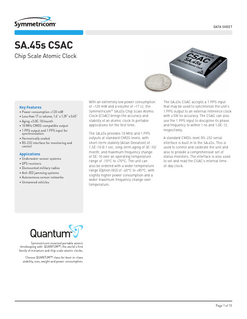
Key Features• Power consumption <120 mW• Less than 17 cc volume, 1.6” x 1.39” x 0.45”• Aging <3.0E-10/month• 10 MHz CMOS-compatible output • 1 PPS output and 1 PPS input for synchronization • Hermetically sealed• RS-232 interface for monitoring and controlApplications• Underwater sensor systems • GPS receivers• Dismounted military radios • Anti-IED jamming systems • Autonomous sensor networks • Unmanned vehiclesWith an extremely low power consumption of <120 mW and a volume of <17 cc, the Symmetricom ® SA.45s Chip Scale Atomic Clock (CSAC) brings the accuracy and stability of an atomic clock to portable applications for the first time.The SA.45s provides 10 MHz and 1 PPS outputs at standard CMOS levels, with short-term stability (Allan Deviation) of 1.5E-10 @ 1 sec, long-term aging of 3E-10/month, and maximum frequency change of 5E-10 over an operating temperature range of -10°C to +70°C. The unit can also be ordered with a wider temperature range (Option 002) of -40°C to +85°C, with slightly higher power consumption and a wider maximum frequency change over temperature.SA.45s CSACChip Scale Atomic ClockThe SA.45s CSAC accepts a 1 PPS input that may be used to synchronize the unit’s 1 PPS output to an external reference clock with ±100 ns accuracy. The CSAC can also use the 1 PPS input to discipline its phase and frequency to within 1 ns and 1.0E-12, respectively.A standard CMOS-level RS-232 serial interface is built in to the SA.45s. This is used to control and calibrate the unit and also to provide a comprehensive set of status monitors. The interface is also used to set and read the CSAC’s internal time-of-day clock.DATA SHEETSymmetricom invented portable atomictimekeeping with QUANTUM™, the worldʼs first family of miniature and chip scale atomic clocks.Choose QUANTUM™ class for best-in-class stability, size, weight and power consumption.Low Power Consumption By Design Every part of the SA.45s CSAC has been engineered for low power consumption.It starts with the physics package, shown here in a cutaway view. A vertical-cavity surface-emitting laser (VCSEL) that has been highly optimized for this specific application illuminates the atomic vapor resonance cell, and the light that gets through the cell is then detected by the photodetector. The photodetector output signal drives a feedback loop which is used to achieve atomic resonance using the principles of coherent population trapping (CPT).The entire physics package has a volume of only 0.35 cm3, and the actual resonance cell itself has a volume of only 2 mm3. It is this extremely small size, plus the fact that it is surrounded by a vacuum within the physics package, that allows the entire physics package to be powered by about 15 mW. As the cutaway drawing shows, the only way the physics package connects with the outside world is through a top and bottom polyimide suspension. All signals that need to go to or from the center stack-up are carried on traces that are printed on the suspensions. And because the suspensions are connected to a frame that is engineered to be slightly shorter than the center stack-up, they are in tension and serveto hold the stack-up in place. The resultis a very small, highly thermally isolated, and robust physics package with excellent performance. All of the electronics that surround the physics package, and which turn it into a fully functional clock, have also been engineered for low power consumption. Even the CSAC controller’s firmware routines have been optimized for low power consumption.Low Power Is Just The BeginningAn atomic clock that consumes only 120mW of power (125 mW for option 002)instead of 10 W or more gives systemdesigners a new and important degree offreedom. But that is just the beginning.Because of its small size and high thermalisolation, the SA.45s CSAC warms up in<130 sec, compared to 8 minutes or morefor conventional atomic clocks. Also, powerconsumption during warm-up is only 140mW, while conventional atomic clocks willoften consume two times their steady-state power during warm-up. Finally, theCSAC’s power consumption variation vs.temperature is negligible, while otheratomic clocks can show variations of 200%or more across their specified temperaturerange.The World's Smallest Atomic ClockPower consumption and size are bothcritical to enabling portable applications,and the SA.45s is by far the smallestatomic clock available. For example, whilethe SA.45s CSAC does not quite equal theperformance of Symmetricom’s XPROrubidium oscillator, the figure shows ithas approximately 1/30th the volume—and1/14th the weight—of the XPRO. Conversely,the SA.45s has much higher performancethan OCXOs, and still offers a 4x reductionin volume compared to popular OCXOpackage sizes.SA.45s CSAC is1/30th the volumeof the XPROS A.45s C S A CX P R O030510152025The SA.45s CSAC is approximatelyUnderwater Sensor Systems Underwater sensors are used in seismic research, oil exploration and many other applications. Sensors designed to lie on the ocean floor will typically include a hydrophone, a geophone and a very stable clock to time-stamp the data collectedby the sensor. Because GPS signals can’t penetrate water, oven-controlled crystal oscillators (OCXO’s) have been used to provide the accuracy needed for most time-stamping applications.But the SA.45s CSAC is a nearly ideal clock for these underwater applications. Because it consumes 1/10th to 1/30th the power ofan OCXO, it requires much less battery power, resulting in smaller and lower-cost sensors, or alternatively, sensors with a much longer mission life.The SA.45s CSAC’s aging rate, which can be 1/100th of even a good OCXO, means that time-stamping errors caused by drift are greatly reduced. Finally, the SA.45s CSAC’s superior temperature coefficient means that when sensors are calibrated to GPS on a warm boat deck, but then dropped into cold ocean water of several hundred meters depth, the offset error produced by this temperature change is minimized.Portable Military SystemsMany advancements in military electronics are aimed at bringing the networked battlefield to the tactical edge, i.e. the individual warfighter. But there are limitations on how many pieces of gear and how much battery weight a warfighter can be expected to carry. This is especially true when operations are carried out in rugged terrain and/or high altitude. The CSAC’s small size, light weight, and extremely low power consumption can help in a number of systems: Dismounted IED Jammers: size and weight are always at a premium, so the SA.45s CSAC is an attractive option. Also, power not applied to the timing subsystem is power that can be applied to the jammer itself, or that can be used to extend mission life. The CSAC's precise synchronizationis critical to prevent self-jamming, whileits ultra-stable holdover is equally vital in GPS-denied environments.Dismounted Radio Systems: the SA.45s CSAC helps to minimize size, weight, and power consumption. At the same time,it provides the high accuracy required by many modern high-bandwidth waveforms, and it provides the stability needed to maintain network synchronization in GPS-denied environments.GPS Receivers: using the SA.45s CSAC as a timebase, military GPS receivers can achieve greatly reduced Time To Subsequent Fix (TTSF) for 24 hours or more. It also becomes possible to operate with only three satellites in view (instead of the usual 4), a distinct advantage in manyurban settings.Unmanned Aerial VehiclesAs the number of applications for civil and military umanned aerial vehicles (UAVs) rapidly expands, the suppliers of payloads for these vehicles are being pressured to increase their functionality. In doing so, they find themselves bumping into limitations in size, weight and power.The SA.45s CSAC can help in all threeareas, with a volume of <17 cm³, a weight of <35 g and power consumption of <125 mW. In fact, in some applications the CSAC is attractive solely because, when compared to conventional rubidium oscillators(~20 W in warm-up, ~10 W in steady state), its low power consumption simplifies thermal management issues.Many UAV’s rely on GPS, and the SA.45s CSAC can be disciplined by the 1 PPS output from a GPS receiver, and provide a stable signal that can be used by C4I or SIGINT payloads. And of course, should GPS be lost due to natural interference or jamming, the SA.45s CSAC provides a stable holdover signal that meets the requirements of even long-endurancemissions.1 Tune2 N/A3 N/A4 BITE5 Tx6 Rx7 Vcc8 GND 91 PPS IN 10 1 PPS OUT 11 N/A 1210 MHz OUTPIN NO. FUNCTIONMechanical InterfaceOptions to Meet a Wider Range of ApplicationsThe standard SA.45s CSAC (options 001 and 002) provides an output frequency of 10MHz. However, other frequencies are available: option 006 provides a 5 MHz output, option 003 provides 16.384 MHz, and option 004 provides 10.24 MHz. Other frequencies are also possible; contact Symmetricom for details.For applications where the very best Allan Deviation (ADEV) is not required, the SA.45s CSAC is also available with less stringent ADEV specifications at a lower price. For example, at TAU = 1sec, option 001 has an ADEV specification of 1.5E-10, while option 101 has a specification of 3E-10....................................................................................................................................................................ELECTRICAL SPECIFICATIONS-001 -002RF Outptut - Frequency: 10 MHz 10 MHz - Format: CMOS CMOS - Amplitude:0V to Vcc 0V to Vcc - Load impedance: 1 MΩ 1 MΩ- Quantity: 1 11 PPS Output- Rise/fall time (10%-90%)at load capacitance 10pF: <10 ns <10 ns - Pulse width: 400 µs 400 µs - Level:0V to Vcc 0V to Vcc - Logic High (V OH ) min: 2.80 V 2.80 V - Logic Low (V OL ) max: 0.30 V 0.30 V - Load impedance: 1 MΩ 1 MΩ- Quantity: 111 PPS Input - Format: Rising edge Rising edge - Low level: <0.5 V<0.5 V- High level:2.5 V to Vcc 2.5 V to Vcc - Input impedance: 1 MΩ 1 MΩ- Quantity:1 1Serial Communications - Protocol: RS232RS232- Format:CMOS 0V to Vcc CMOS 0V to Vcc - Tx/Rx impedance: 1 MΩ 1 MΩ- Baud rate:57600 57600Built-in Test Equipment (BITE) output - Format: CMOS 0V to Vcc CMOS 0V to Vcc - Load impedance: 1 MΩ 1 MΩ- Logic: 0 = Normal operation 0 = Normal operation 1 = Alarm 1 = Alarm Power Input - Operating: <120 mW <125 mW - Warmup:<140 mW <140 mW - Input voltage (Vcc):3.3 ± 0.1 VDC3.3 ± 0.1 VDCPHYSICAL SPECIFICATIONS- Size: 1.6” x 1.39” x 0.45” 1.6” x 1.39” x 0.45”- Weight: <35 g<35 g- MTBF:>100,000 hours>50,000 hoursENVIRONMENTAL SPECIFICATIONSOperating:- Operating temperature: -10°C to +70°C -40°C to +85°C- Maximum frequency change over operating temp range (max. rate of change 0.5 °C/minute): 5x10⁻¹⁰ 1x10⁻⁹- Frequency change over allowable input voltage range: <4x10⁻¹⁰<4x10⁻¹⁰ENVIRONMENTAL SPECIFICATIONS (Continued)-001 -002- Magnetic sensitivity(≤2.0 Gauss):<9x10-11/Gauss <9x10-11/Gauss - Radiated emissions: Compliant to FCC Compliant to FCC part 15, Class B, part 15, Class B, when mounted when mounted properly onto properly ontohost PCB.host PCB.- Vibration: Maintains lock under Maintains lock under MIL-STD-810, MIL-STD-810, Method 514.5,Method 514.5,Procedure 1, 7.7 grms Procedure 1, 7.7 grms - Humidity: 0 to 95% RH per 0 to 95% RH per MIL-STD-810, MIL-STD-810,Method 507.4.Method 507.4Storage and Transport (non-operating):- Temperature: - 55°C to +90°C - 55°C to +90°C - Shock (1 ms half-sine): 1000 g 1000 g- Vibration: MIL-STD-810, MIL-STD-810, Method 514.5, Method 514.5,Procedure 1, 7.7 grmsProcedure 1, 7.7 grmsPERFORMANCE PARAMETERSStability (Allan Deviation) ADEVTAU = 1 sec 1.5x10⁻¹⁰ 2x10⁻¹⁰TAU = 10 sec 5x10-11 7x10-11TAU = 100 sec 1.5x10⁻¹¹ 2x10-11TAU = 1000 sec5x10-127x10-12RF Output Phase Noise (SSB)1 Hz <-50 dBc/Hz <-50 dBc/Hz 10 Hz <-70 dBc/Hz <-70 dBc/Hz 100 Hz <-113 dBc/Hz <-113 dBc/Hz 1000 Hz <-128 dBc/Hz <-128 dBc/Hz 10000 Hz <-135 dBc/Hz <-135 dBc/Hz 100,000 Hz<-140 dBc/Hz <-140 dBc/HzFrequency Accuracy- Maximum offset at shipment: ±5x10-11 ±5x10-11- Maximum retrace (48 hrs off): ±5x10-11 ±5x10-11- A ging, monthly*: <3x10⁻¹⁰ <3x10⁻¹⁰- Aging, yearly*: <1x10⁻⁹ <1x10⁻⁹- 1 PPS Sync.: ±100 ns ±100 ns(*After 30 days of continuous operation)Digital Tuning - Range: ±2x10⁻⁸ ±2x10⁻⁸- Resolution: 1x10-12 1x10-12Analog Tuning - Range: ±2.2x10⁻⁸ ±2.2x10⁻⁸- Resolution: 1x10-111x10-11- Input: 0-2.5V into 100 kΩ 0-2.5V into 100 kΩWarm-up Time<130 s<180 sSolderHand solder using 63/37 Tin/Lead Solder with maximum soldering tip of 329°C (625°F)SpecificationsPart numbers 090-00218-001 and 090-00218-002All specifications at 25°C, Vcc =3.3VDC unless otherwise specified...................................................................................................................................................................ELECTRICAL SPECIFICATIONS-101 -102RF Outptut - Frequency: 10 MHz 10 MHz - Format: CMOS CMOS - Amplitude:0V to Vcc 0V to Vcc - Load impedance: 1 MΩ 1 MΩ- Quantity: 1 11 PPS Output- Rise/fall time (10%-90%)at load capacitance 10pF: <10 ns <10 ns - Pulse width: 400 µs 400 µs - Level:0V to Vcc 0V to Vcc - Logic High (V OH ) min: 2.80 V 2.80 V - Logic Low (V OL ) max: 0.30 V 0.30 V - Load impedance: 1 MΩ 1 MΩ- Quantity: 111 PPS Input - Format: Rising edge Rising edge - Low level: <0.5 V<0.5 V- High level:2.5 V to Vcc 2.5 V to Vcc - Input impedance: 1 MΩ 1 MΩ- Quantity:1 1Serial Communications - Protocol: RS232RS232- Format:CMOS 0V to Vcc CMOS 0V to Vcc - Tx/Rx impedance: 1 MΩ 1 MΩ- Baud rate:57600 57600Built-in Test Equipment (BITE) output - Format: CMOS 0V to Vcc CMOS 0V to Vcc - Load impedance: 1 MΩ 1 MΩ- Logic: 0 = Normal operation 0 = Normal operation 1 = Alarm 1 = AlarmPower Input - Operating: <120 mW <125 mW - Warmup:<140 mW <140 mW - Input voltage (Vcc):3.3 ± 0.1 VDC3.3 ± 0.1 VDCPHYSICAL SPECIFICATIONS- Size: 1.6” x 1.39” x 0.45” 1.6” x 1.39” x 0.45”- Weight: <35 g<35 g- MTBF:>100,000 hours>50,000 hoursENVIRONMENTAL SPECIFICATIONSOperating:- Operating temperature: -10°C to +70°C -40°C to +85°C- Maximum frequency change over operating temp range (max. rate of change 0.5 °C/minute): 5x10⁻¹⁰ 1x10⁻⁹- Frequency change over allowable input voltage range: <4x10⁻¹⁰<4x10⁻¹⁰ENVIRONMENTAL SPECIFICATIONS (Continued)-101 -102- Magnetic sensitivity(≤2.0 Gauss):<9x10-11/Gauss <9x10-11/Gauss - Radiated emissions: Compliant to FCC Compliant to FCC part 15, Class B, part 15, Class B, when mounted when mounted properly onto properly ontohost PCB.host PCB.- Vibration: Maintains lock under Maintains lock under MIL-STD-810, MIL-STD-810, Method 514.5,Method 514.5,Procedure 1, 7.7 grms Procedure 1, 7.7 grms - Humidity: 0 to 95% RH per 0 to 95% RH per MIL-STD-810, MIL-STD-810,Method 507.4.Method 507.4Storage and Transport (non-operating):- Temperature: - 55°C to +90°C - 55°C to +90°C - Shock (1 ms half-sine): 1000 g 1000 g- Vibration: MIL-STD-810, MIL-STD-810, Method 514.5, Method 514.5,Procedure 1, 7.7 grmsProcedure 1, 7.7 grmsPERFORMANCE PARAMETERSStability (Allan Deviation)ADEVTAU = 1 sec 3x10⁻¹⁰ 3x10⁻¹⁰TAU = 10 sec 9.5x10⁻¹¹ 9.5x10⁻¹¹TAU = 100 sec 3x10-11 3x10-11TAU = 1000 sec9.5x10-129.5x10⁻¹²RF Output Phase Noise (SSB)1 Hz <-50 dBc/Hz <-50 dBc/Hz 10 Hz <-70 dBc/Hz <-70 dBc/Hz 100 Hz <-113 dBc/Hz <-113 dBc/Hz 1000 Hz <-128 dBc/Hz <-128 dBc/Hz 10000 Hz <-135 dBc/Hz <-135 dBc/Hz 100,000 Hz<-140 dBc/Hz <-140 dBc/HzFrequency Accuracy- Maximum offset at shipment: ±5x10-11 ±5x10-11- Maximum retrace (48 hrs off): ±5x10-11 ±5x10-11- A ging, monthly*: <3x10⁻¹⁰ <3x10⁻¹⁰- Aging, yearly*: <1x10⁻⁹ <1x10⁻⁹- 1 PPS Sync.: ±100 ns ±100 ns(*After 30 days of continuous operation)Digital Tuning - Range: ±2x10⁻⁸ ±2x10⁻⁸- Resolution: 1x10-12 1x10-12Analog Tuning - Range: ±2.2x10⁻⁸ ±2.2x10⁻⁸- Resolution: 1x10-111x10-11- Input: 0-2.5V into 100 kΩ 0-2.5V into 100 kΩWarm-up Time<130 s<180 sSolderHand solder using 63/37 Tin/Lead Solder with maximum soldering tip of 329°C (625°F)SpecificationsPart numbers 090-00218-101 and 090-00218-102All specifications at 25°C, Vcc =3.3VDC unless otherwise specifiedPart numbers 090-00218-003 and 090-00218-103..................................................................................................................................................................................................................................SpecificationsELECTRICAL SPECIFICATIONS RF Outptut - Frequency: 16.384 MHz - Format: CMOS - Amplitude: 0V to Vcc - Load impedance: 1 MΩ - Quantity: 11 PPS Output - Rise/fall time (10%-90%) at load capacitance 10pF: <10 ns - Pulse width: 400 µs - Level: 0V to Vcc - Logic High (V OH ) min: 2.80 V - Logic Low (V OL ) max: 0.30 V - Load impedance: 1 MΩ - Quantity: 1 1 PPS Input - Format: Rising edge - Low level: <0.5 V - High level: 2.5 V to Vcc - Input impedance: 1 MΩ - Quantity: 1 Serial Communications - Protocol: RS-232 - Format: CMOS 0V to Vcc - Tx/Rx impedance: 1 MΩ - Baud rate: 57600 Built-in Test Equipment (BITE) output - Format: CMOS 0V to Vcc - Load impedance: 1 MΩ - Logic: 0 = Normal operation 1 = Alarm Power Input - Operating: <120 mW - Warmup: <140 mW - Input Voltage (Vcc): 3.3 ± 0.1 VDC All specifications at 25°C, Vcc =3.3VDC unless otherwise specifiedPHYSICAL SPECIFICATIONS- Size:1.6” x 1.39” x 0.45”- Weight: <35 g- MTBF:>100,000 hoursENVIRONMENTAL SPECIFICATIONSOperating:- Operating temperature: -10°C to +70°C- Maximum frequency change over operating temp range (max. rate of change 0.5°C/minute):5x10-10- Frequency change over allowable input voltage range:<4x10⁻¹⁰- Magnetic sensitivity (≤2.0 Gauss):<9x10-11/Gauss - Radiated emissions: Compliant to FCC part 15, Class B, when mounted properlyonto host PCB- Vibration: Maintains lock under MIL-STD-810, method 514.5, procedure 1,7.7 grms- Humidity: 0 to 95% RH per MIL-STD-810, method 507.4Storage and Transport (non-operating):- Temperature: -55°C to +90°C - Shock (1 ms half-sine): 1000 g - Vibration:M IL-STD-810, method 514.5, procedure 1, 7.7 grmsPERFORMANCE PARAMETERSStability (Allan Deviation)ADEV -003 -103TAU = 1 sec 1.5x10⁻¹⁰ 3x10⁻¹⁰ TAU = 10 sec 5x10-11 9.5x10⁻¹¹TAU = 100 sec 1.5x10⁻¹¹ 3x10-11TAU = 1000 sec 5x10-129.5x10⁻¹²RF Output Phase Noise (SSB)1 Hz <-46 dBc/Hz 10 Hz <-66 dBc/Hz 100 Hz <-110 dBc/Hz 1000 Hz <-128 dBc/Hz 10000 Hz <-135 dBc/Hz 100,000 Hz<-140 dBc/HzFrequency Accuracy- Maximum offset at shipment: ±5x10-11- Maximum retrace (48 hrs off): ±5x10-11 - Aging, monthly*: <3x10⁻¹⁰ - Aging, yearly*: <1x10⁻⁹ - 1 PPS sync.: ±100 ns (*After 30 days of continuous operation)Digital Tuning - Range: ±2x10⁻⁸- Resolution: 1x10-12Analog Tuning - Range: ±2.2x10⁻⁸ - Resolution: 1x10-11- Input: 0 - 2.5V into 100 kΩWarm-up Time<130 sSolderHand solder using 63/37 Tin/Lead Solder with maximum soldering tip of 329°C (625°F)Part numbers 090-00218-004 and 090-00218-104..................................................................................................................................................................................................................................SpecificationsELECTRICAL SPECIFICATIONS RF Outptut - Frequency: 10.24 MHz - Format: CMOS - Amplitude: 0V to Vcc - Load impedance: 1 MΩ - Quantity: 11 PPS Output - Rise/fall time (10%-90%) at load capacitance 10pF: <10 ns - Pulse width: 400 µs - Level: 0V to Vcc - Logic High (V OH ) min: 2.80 V - Logic Low (V OL ) max: 0.30 V - Load impedance: 1 MΩ - Quantity: 1 1 PPS Input - Format: Rising edge - Low level: <0.5 V - High level: 2.5 V to Vcc - Input impedance: 1 MΩ - Quantity: 1 Serial Communications - Protocol: RS-232 - Format: CMOS 0V to Vcc - Tx/Rx impedance: 1 MΩ - Baud rate: 57600 Built-in Test Equipment (BITE) output - Format: CMOS 0V to Vcc - Load impedance: 1 MΩ - Logic: 0 = Normal operation 1 = Alarm Power Input - Operating: <120 mW - Warmup: <140 mW - Input Voltage (Vcc): 3.3 ± 0.1 VDC All specifications at 25°C, Vcc =3.3VDC unless otherwise specifiedPHYSICAL SPECIFICATIONS- Size:1.6” x 1.39” x 0.45”- Weight: <35 g- MTBF:>100,000 hoursENVIRONMENTAL SPECIFICATIONSOperating:- Operating temperature: -10°C to +70°C- Maximum frequency change over operating temp range (max. rate of change 0.5°C/minute):5x10-10- Frequency change over allowable input voltage range:<4x10⁻¹⁰- Magnetic sensitivity (≤2.0 Gauss):<9x10-11/Gauss - Radiated emissions: Compliant to FCC part 15, Class B, when mounted properlyonto host PCB- Vibration: Maintains lock under MIL-STD-810, method 514.5, procedure 1,7.7 grms- Humidity: 0 to 95% RH per MIL-STD-810, method 507.4Storage and Transport (non-operating):- Temperature: -55°C to +90°C - Shock (1 ms half-sine): 1000 g - Vibration:M IL-STD-810, method 514.5, procedure 1, 7.7 grmsPERFORMANCE PARAMETERSStability (Allan Deviation)ADEV -004 -104TAU = 1 sec 1.5x10⁻¹⁰ 3x10⁻¹⁰ TAU = 10 sec 5x10-11 9.5x10⁻¹¹TAU = 100 sec 1.5x10⁻¹¹ 3x10-11TAU = 1000 sec 5x10-129.5x10⁻¹²RF Output Phase Noise (SSB)1 Hz <-50 dBc/Hz 10 Hz <-70 dBc/Hz 100 Hz <-113 dBc/Hz 1000 Hz <-128 dBc/Hz 10000 Hz <-135 dBc/Hz 100,000 Hz<-140 dBc/HzFrequency Accuracy- Maximum offset at shipment: ±5x10-11- Maximum retrace (48 hrs off): ±5x10-11 - Aging, monthly*: <3x10⁻¹⁰ - Aging, yearly*: <1x10⁻⁹ - 1 PPS sync.: ±100 ns (*After 30 days of continuous operation)Digital Tuning - Range: ±2x10⁻⁸- Resolution: 1x10-12Analog Tuning - Range: ±2.2x10⁻⁸ - Resolution: 1x10-11- Input: 0 - 2.5V into 100 kΩWarm-up Time<130 sSolderHand solder using 63/37 Tin/Lead Solder with maximum soldering tip of 329°C (625°F)Part numbers 090-00218-006 and 090-00218-106................................................................................................................................................................................................................................SpecificationsELECTRICAL SPECIFICATIONS RF Outptut - Frequency: 5 MHz - Format: CMOS - Amplitude: 0V to Vcc - Load impedance: 1 MΩ - Quantity: 11 PPS Output - Rise/fall time (10%-90%) at load capacitance 10pF: <10 ns - Pulse width: 400 µs - Level: 0V to Vcc - Logic High (V OH ) min: 2.80 V - Logic Low (V OL ) max: 0.30 V - Load impedance: 1 MΩ - Quantity: 1 1 PPS Input - Format: Rising edge - Low level: <0.5 V - High level: 2.5 V to Vcc - Input impedance: 1 MΩ - Quantity: 1 Serial Communications - Protocol: RS-232 - Format: CMOS 0V to Vcc - Tx/Rx impedance: 1 MΩ - Baud rate: 57600 Built-in Test Equipment (BITE) output - Format: CMOS 0V to Vcc - Load impedance: 1 MΩ - Logic: 0 = Normal operation 1 = Alarm Power Input - Operating: <120 mW - Warmup: <140 mW - Input Voltage (Vcc): 3.3 ± 0.1 VDC All specifications at 25°C, Vcc =3.3VDC unless otherwise specifiedPHYSICAL SPECIFICATIONS- Size:1.6” x 1.39” x 0.45”- Weight: <35 g- MTBF:>100,000 hoursENVIRONMENTAL SPECIFICATIONSOperating:- Operating temperature: -10°C to +70°C- Maximum frequency change over operating temp range (max. rate of change 0.5°C/minute):5x10-10- Frequency change over allowable input voltage range:<4x10⁻¹⁰- Magnetic sensitivity (≤2.0 Gauss):<9x10-11/Gauss - Radiated emissions: Compliant to FCC part 15, Class B, when mounted properlyonto host PCB- Vibration: Maintains lock under MIL-STD-810, method 514.5, procedure 1,7.7 grms- Humidity: 0 to 95% RH per MIL-STD-810, method 507.4Storage and Transport (non-operating):- Temperature: -55°C to +90°C - Shock (1 ms half-sine): 1000 g - Vibration:M IL-STD-810, method 514.5, procedure 1, 7.7 grmsPERFORMANCE PARAMETERSStability (Allan Deviation)ADEV -006 -106TAU = 1 sec 1.5x10⁻¹⁰ 3x10⁻¹⁰ TAU = 10 sec 5x10-11 9.5x10⁻¹¹TAU = 100 sec 1.5 x10⁻¹¹ 3 x10-11TAU = 1000 sec 5x10-129.5x10⁻¹²RF Output Phase Noise (SSB)1 Hz <-53 dBc/Hz 10 Hz <-73 dBc/Hz 100 Hz <-116 dBc/Hz 1000 Hz <-131 dBc/Hz 10000 Hz <-138 dBc/Hz 100,000 Hz<-140 dBc/HzFrequency Accuracy- Maximum offset at shipment: ±5x10-11- Maximum retrace (48 hrs off): ±5x10-11 - Aging, monthly*: <3x10⁻¹⁰ - Aging, yearly*: <1x10⁻⁹ - 1 PPS sync.: ±100 ns (*After 30 days of continuous operation)Digital Tuning - Range: ±2x10⁻⁸- Resolution: 1x10-12Analog Tuning - Range: ±2.2x10⁻⁸ - Resolution: 1x10-11- Input: 0 - 2.5V into 100 kΩWarm-up Time<130 sSolderHand solder using 63/37 Tin/Lead Solder with maximum soldering tip of 329°C (625°F)SA.45s CSAC2300 Orchard Parkway © 2012 Symmetricom. Symmetricom and the Symmetricom logo are registered trademarks。
- 1、下载文档前请自行甄别文档内容的完整性,平台不提供额外的编辑、内容补充、找答案等附加服务。
- 2、"仅部分预览"的文档,不可在线预览部分如存在完整性等问题,可反馈申请退款(可完整预览的文档不适用该条件!)。
- 3、如文档侵犯您的权益,请联系客服反馈,我们会尽快为您处理(人工客服工作时间:9:00-18:30)。
SA.45s芯片级原子钟
产品概述
Symmetricom芯片级原子钟,SA.45s功耗低至 <115 mW,其体积只有<16 cc,提供超低功耗工作模式的设置。
此模式下,其物理封装通常是关闭状态,器件工作于类似TCXO自由振荡的状态,当物理封装定期启动后,重新驯服TCXO(不超过120s),这种模式下的平均功耗不超过50 mW。
第一次让便携仪表也可拥有原子钟水平的准确性及稳定性。
西安同步电子科技有限公司有售
产品功能Array
1)提供一路标准的10MHz正弦信号;
2)同步的1 PPS输入/输出;
3)RS-232管理控制接口。
产品特点
a)超低功耗节电模式,<100 mW;
b)全密闭封装;
c)超小体积,高可靠性。
典型应用
1)水下传感器网络;
2)GPS接收机;
3)背负式电台;
4)反简易爆炸装置(Anti-IED)干扰系统;
5)独立传感器网络无人驾驶飞机等。
技术指标
安装尺寸:。