低功率霍尔集成电路开关TLE4917
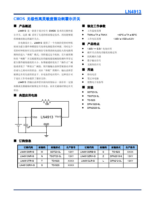
LN4913_C南麟中文版规格书CMOS 无极性高灵敏度微功耗霍尔开关
1.000
1.200
0.800
1.000
0.200MIN
0.200
0.300
0.500TYP
0.174
0.326
Dimensions In Inches
Min
Max
0.014
0.018
0.000
0.002
0.005REF
0.056
0.062
0.076
0.082
0.039
0.047
0.031
0.039
VDD 1 VOUT 2
3 GND
DFN2020-3L (TOP VIEW)
SOT23-3L/TSOT23-3L 2 3 1 -
引脚号 DFN1520-6L
5 3 2 1,4,6
Sensitive Area (感应区)
DFN2020-3L 2 3 1 -
TO-92S (Front View)
引脚名
VOUT GND VDD NC
CMOS 无极性高灵敏度微功耗霍尔开关
LN4913
■ 产品概述
LN4913 是一款基于混合信号 CMOS 技术的无极性霍 尔开关,这款 IC 采用了先进的斩波稳定技术,因而能够提 供准确而稳定的磁开关点。
在电路设计上,LN4913 提供了一个内嵌的受控时钟机 制来为霍尔器件和模拟信号处理电路提供时钟源,同时这个 受控时钟机制可以发出控制信号使得消耗电流较大的电路周 期性的进入“休眠”模式;同样通过这个机制,芯片被周期 性的“唤醒”并且根据预定好的磁场强度阈值检测外界穿过 霍尔器件磁场强度的大小。如果磁通密度高于“操作点”阈 值或者低于“释放点”阈值,则开漏输出晶体管被驱动并锁 存成与之相对应的状态。而在“休眠”周期中,输出晶体管 被锁定在其先前的状态下。在电池供电应用中,这种设计对 于延长工作寿命提供了最好支持。
CC6111高精度低温漂单极型霍尔效应开关数据手册说明书

CC6111具有斩波稳定功能的高精度,低温漂单极型霍尔效应开关概述CC6111是一个单极型的霍尔效应开关IC ,采用先进的BiCMOS 制程制造,具有优异的温度稳定性和很高的抗机械应力性能,产品最高工作温度可以达到150℃。
CC6111采用动态失调消除技术以及芯进电子专利保护的温度补偿技术,大幅降低了由于封装应力,环境温度变化等因素造成的失调电压,使产品磁灵敏度持高度的一致性。
CC6111包含稳压输出模块,霍尔薄片,信号放大模块,动态失调消除模块以及带有限流保护的功率输出级。
内置的稳压输出电路模块可以让芯片工作在2.5V 至28V 电源电压范围。
CC6111提供TO-92S 和TSOT23-3两种封装,均为符合RoHS 规范,产品的使用环境温度范围为-40~150℃。
功能框图特点◆ 工作范围宽,2.5~28V◆ 反向电压保护,最高可到 - 40V◆ 具有斩波稳定功能,批次之间的一致性好◆ 30V 过压保护,避免IC 因电源电压脉冲而损坏 ◆ 温度稳定性优异,可工作到150℃ ◆ 输出级限流保护30mA◆ 输出级36V 过压保护,避免输出脚被干扰电压击穿 ◆ 小尺寸,TO-92S 和TSOT23-3封装◆ 抗机械应力◆ ESD HBM 4000V 应用◆ 直流无刷马达 ◆ 速度检测 ◆ 线性位置检测 ◆角度检测名称 封装型号 备注 CC6111TO TO-92S 袋装,1000片/包 CC6111STTSOT23-3卷盘,3000片/卷开关输出 vs. 磁场极性注意: 磁场加在芯片的丝印面管脚描述名称管脚编号功能 TO-92STSOT23-3V DD 1 1 电源电压 GND 2 3 地 V OUT32输出参数符号数值单位电源电压V DD30 V反向耐压V RDD-40 V持续电流I OUT30 mA输出脚耐压V OUT30 V磁场强度 B 无限制Gauss工作环境温度T A-40~150 ℃存储环境温度Ts -50至160 ℃ESD(HBM) 4000 V电气参数参数符号测试环境最小值典型值最大值单位电源电压V DD- 2.5 - 28.0 V静态电流I DD25 ℃,V DD=12V - 2 - mA输出饱和压降V SAT25 ℃,I OUT=20mA - - 0.4 V输出限流值I limit30 - 60 mA上升时间tr R L=820Ω,C L=20pF - 0.2 - us下降时间tf R L=820Ω,C L=20pF - 0.1 - us反向电流I RDD V DD=-40V - - 5 mA磁参数参数符号测试环境最小值典型值最大值单位工作点B OP25 ℃30 40 50 Gauss释放点B RP25 ℃20 30 40 Gauss迟滞B HYS25 ℃ 5 10 15 Gauss典型应用电路0123405101520253035I D D (m A )VDD (V)静态电流 vs. 工作电压磁感应点 vs. 工作电压磁感应点 vs. 温度(1)TO-92S packageHall 感应点位置注意: 所有单位均为毫米。
霍尔元件简介
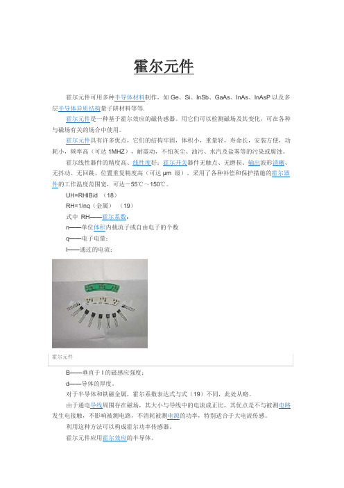
2工作原理霍尔元件应用霍尔效应的半导体。
所谓霍尔效应,是指磁场作用于载流金属导体、半导体中的载流子时,产生横向电位差的物理现象。
金属的霍尔效应是1879年被美国物理学家霍尔发现的。
当电流通过金属箔片时,若在垂直于电流的方向施加磁场,则金属箔片两侧面会出现横向电位差。
半导体中的霍尔效应比金属箔片中更为明显,而铁磁金属在居里温度以下将呈现极强的霍尔效应。
利用霍尔效应可以设计制成多种传感器。
霍尔电位差UH的基本关系为:UH=RHIB/d (1)RH=1/nq(金属)(2)式中RH――霍尔系数;n――单位体积内载流子或自由电子的个数;q――电子电量;I――通过的电流;B――垂直于I的磁感应强度;d――导体的厚度。
对于半导体和铁磁金属,霍尔系数表达式和式(2)不同,此处从略。
由于通电导线周围存在磁场,其大小和导线中的电流成正比,故可以利用霍尔元件测量出磁场,就可确定导线电流的大小。
利用这一原理可以设计制成霍尔电流传感器。
其优点是不和被测电路发生电接触,不影响被测电路,不消耗被测电源的功率,特别适合于大电流传感。
若把霍尔元件置于电场强度为E、磁场强度为H的电磁场中,则在该元件中将产生电流I,元件上同时产生的霍尔电位差和电场强度E成正比,如果再测出该电磁场的磁场强度,则电磁场的功率密度瞬时值P可由P=EH确定。
利用这种方法可以构成霍尔功率传感器。
如果把霍尔元件集成的开关按预定位置有规律地布置在物体上,当装在运动物体上的永磁体经过它时,可以从测量电路上测得脉冲信号。
根据脉冲信号列可以传感出该运动物体的位移。
若测出单位时间内发出的脉冲数,则可以确定其运动速度。
[1]3元件特性1、霍尔系数(又称霍尔常数)RH在磁场不太强时,霍尔电势差UH与激励电流I和磁感应强度B的乘积成正比,与霍尔片的厚度δ成反比,即UH =RH*I*B/δ,式中的RH称为霍尔系数,它表示霍尔效应的强弱。
另RH=μ*ρ即霍尔常数等于霍尔片材料的电阻率ρ与电子迁移率μ的乘积。
SP490_491E_cn
增强型全双工RS-485收发器-SP490E/SP491Ez+5V的电压z低功耗BiCMOS工艺制造z驱动器/接收器使能(SP491E)z RS-485和RS-422驱动器/接收器z管脚兼容LTC490和SN75179(SP490E)z管脚兼容LTC491和SN75180(SP491E)z增强型ESD规范:±15kV人体放电模式(Human Body Model)±15kV IEC1000-4-2 气隙放电(Air Discharge)±8kV IEC1000-4-2 接触放电(Contact Discharge)描述SP490E是一个低功耗差分收发器,满足RS-485和RS-422标准规范,数据传输速率高达10Mbps。
除了增加了驱动器和接收器三态使能线外,SP491E和SP490E完全相同。
在共模模式的限制范围内,两者的接收器输入的灵敏度为±200mV。
SP490E包含8脚塑料DIP和8脚NSOIC两种封装形式,可工作在商业级和工业级温度范围内。
SP491E包含14脚DIP和14脚NSOIC两种封装,也可工作在商业级和工业级温度范围内。
S P490E绝对最大额定值下面列出的是器件正常工作的额定值,并未涉及器件在这些条件或超出这些条件下的功能操作。
器件不能长时间工作在绝对最大额定值条件下,否则会影响其可靠性。
Vcc………………………………………………………………………………………………………..+7V输入电压驱动器 ……………………………………………………………………………-0.5V~(Vcc+0.5V) 接收器……………………………………………………………………………………………..±14V输出电压驱动器 ……………………………………………………………………………………………±14V接收器……………………………………………………………………………… -0.5~(Vcc+0.5V)贮存温度…………………………………………………………………………………….-65℃~+150℃功耗…………………………………………………………………………………………………..1000mW参数规范除非特别说明,T~T和Vcc=5V±5﹪续上表图1 驱动器DC 测试负载电路 图2 接收器时序测试负载电路C图3 驱动器/接收器时序测试电路 图4 驱动器时序测试负载#2电路图5 驱动器传输延时Y, ZY, Z图6 驱动器使能和禁能时间图7 接收器传输延时绝对最大额定值下面列出的是器件正常工作的额定值,并未涉及器件在这些条件或超出这些条件下的功能操作。
LST248全级型微功耗霍尔开关介绍及电路图

48 -- EST248; Y – 年; M -- “A”-“Z”, 月 ; X– 批次;
封装形式
UA( TO-92S) SO(SOT-23) ST(TSOT-23) DF(DFN2020-3)
磁场特性 LH248 参数 Bop Brp Bhys
最小值 -
+/-0.5 -
管脚说明 管脚名称 Vdd Out Gnd
序号 1 2 3
5V 5mA 5V 5mA -40~85℃ -55~150℃
最小值 2.5
典型值 2.75 5
175
最大值 3.5
1 0.4
70
单位 V uA mA V uS mS
LH248
CMOS 全极性高灵敏度低功耗霍尔开关
描述 LH248 是一款基于混合信号 CMOS 技术的全极性霍尔效应传感器,这款 IC 采用了先
进的斩波稳定技术,因而能够提供准确而稳定的磁开关点。 在电路设计上,LH248 提供了一个内嵌的受控时钟机制来为霍尔器件和模拟信号处理
电路提供时钟源,同时这个受控时钟机制可以发出控制信号 使得消耗电流较大的电路 周期 性的进入“休眠”模式;同样通过这个机制,芯片被周期性的“唤醒”并且根据预定好的磁 场强度阈值检测外界穿过霍尔器件磁场强度的大小。如果磁通密度高于“执行点”阈值或者 低于“释放点”阈值,则开漏输出晶体管被驱动并锁存成与之相对应的状态。而在“休眠” 周期中,输出晶体管被锁定在其先前的状态下。在电池供电应用中,这种设计对于延长工作 寿命提供了最好支持。
2.3.± 0.1
2.13 1.87
1.00 1.20
1
2
3
Sensor Location
Active Area Depth:
Melexis霍尔原件分类
Triaxis三轴霍尔芯片部件编号说明2SA-10 Integrated 2-Axis Hall SensorCSA-1V Current SensorMLX90316 旋转角度位置传感器芯片MLX90324 "在引擎罩下"旋转位置传感器,支持SENT 协议MLX90324 archive Under-the-Hood Rotary Position sensor, feat. SENT protocolMLX90333 Triaxis™3D-Joystick Position SensorMLX91205 Current Sensor传感器芯片:霍尔效应MLX90324 "在引擎罩下"旋转位置传感器,支持SENT 协议MLX90324_archive Under-the-Hood Rotary Position sensor, feat. SENT protocol特殊用途霍尔芯片MLX90217 凸轮传感器MLX90224 Dual Hall Effect LatchMLX90248 (New Generation) Micropower & Omnipolar Hall Switch-Very High Sensitivity MLX90254 差分动态霍尔效应传感器线性霍尔芯片MLX90215 Precision Programmable Linear Hall ICMLX90242 Linear Hall Effect SensorMLX90251 可编程的线性霍尔效应传感器MLX90277 Dual Programmable Linear Hall Effect Sensor霍尔效应单极开关US5781 单极霍尔开关- 中等灵敏度US5782 单极霍尔开关-中等灵敏度US5881 单极霍尔开关-低灵敏度霍尔效应双极开关US2881 双极霍尔开关-非常高的灵敏度US2882 双极霍尔开关-非常高的灵敏度US2884 双极霍尔开关-非常高的灵敏度US4881 双极霍尔开关-低压& 非常高的灵敏度霍尔效应锁闩器US1881 霍尔闩锁器–高度灵敏度US3881 霍尔闩锁器–低压&高度灵敏度霍尔效应风扇电机驱动器MLX90283 振动电机驱动器US168 单线圈风扇驱动器-低噪声& 低电压(转速计输出) US169 单线圈风扇驱动器-低噪声& 低电压(报警输出)US62 双线圈风扇驱动器(转速计输出)US63 双线圈风扇驱动器(报警输出)US65 双线圈风扇驱动器-低噪声& 高输出电流(转速计输出) US651 双线圈风扇驱动器-低噪声(转速计输出)US66 双线圈风扇驱动器-低噪声& 高输出电流(报警输出) US661 双线圈风扇驱动器-低噪声(报警输出)US72 单线圈风扇驱动器-高电压(转速计输出)US73 单线圈风扇驱动器-高电压(报警输出)US79 智能风扇电机驱动器US890 双线圈风扇驱动器-高输出电流(转速计输出)US891 双线圈风扇驱动器-高输出电流(报警输出)US90A 双线圈风扇驱动器-高电压(转速计输出)US91A 双线圈风扇驱动器-高电压(报警输出)。
华奥电子 LD497 汽车电子点火控制集成电路说明书
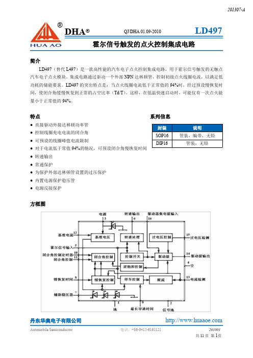
丹东华奥电子有限公司简介LD497(替代L497)是一款高性能的汽车电子点火控制集成电路,用于霍尔信号触发的无触点汽车电子点火模块。
集成电路通过驱动一个外部NPN 达林顿管,控制初级点火线圈电流,以满足低功耗的储能要求。
LD497的突出特点是:当点火线圈电流低于正常值的94%时,经过预设慢恢复时间,使闭合角缓慢恢复到正常的占空比率(Td/T )。
这样,在低温快速启动时,可能仅有一次点火能量小于正常值的94%。
特点系列信息●直接驱动外接达林顿功率管●控制线圈充电电流的闭合角●可预设的线圈峰值电流限制●对于电流低于常值94%的情况,可预设闭合角慢恢复时间●转速输出●常通保护●为保护外部达林顿管设置的过压保护●内置电源保护稳压管●电源反接保护方框图封装说明SOP16管装,编带,无铅DIP16管装,无铅霍尔信号触发的点火控制集成电路丹东华奥电子有限公司绝对最大值热阻*)热阻(结-氧化铝),是指芯片焊接在底层为氧化铝的基片上,尺寸15×20,厚度0.65mm。
管脚连接(顶视图)缩写参数数值单位I 3直流电源电流瞬变电源电流(tf 持续时间=100ms )200800mA mAV 3电源电压内部限压到Vz3V 6转速输出电压28V I 16驱动器集电极直流电流脉冲(t ≤3ms)300600mA mA V 16驱动器集电极电压28V I 7辅助稳压管电流40mA I 15过压稳压管直流电流脉冲(tfall 保持时间=300µs,trep 重复时间≥3ms )1535mA mA V R 电池反接电压,应用电路图4–16V Tj,Tstg 结温和储藏温度范围–55to 150℃P tot功耗Taluminia =90℃SOP-16Tamb =90℃DIP-161.20.65W W 缩写参数数值单位Rth j-amb 热阻(结-环境)DIP16最大值90℃/W Rth j-alumin (*)热阻(结-氧化铝)SOP16最大值50℃/WLD497管脚功能(参考图4)丹东华奥电子有限公司管脚功能(续)(参考图4)电参数(Vs=14.4V,-40℃<Tj<125℃,除非另外说明)丹东华奥电子有限公司电参数(续)(Vs=14.4V,-40℃<Tj<125℃,除非另外说明)注释: 1.td/t去饱和时间比率率为:td/T=1/(1+I11C/I11D)2.当外部达林顿管工作在放大区时,Isense(检测)=Icoil(线圈)功能描述一、闭合角控制闭合角控制电路根据转速、电源电压和初级线圈特性为输出晶体管计算导通时间D。
英飞凌推出采用超小型SOT23封装的高精度高能效TLE496x霍尔传感器

稳压器也非常适合在汽车环境 中工作 ,能承受电池 传感器。 全新 T L E 4 9 6 x 传感器提供全球最小的霍尔 反接情况 、 + 4 3 V负载突降瞬变和双 电池跳 接起动 传感器封装 ( S O T 2 3 ) 。 该产品以英飞凌开发的全新 ( j u m p s t a r t ) 。 这种鲁棒性有助于在恶劣环境中实现
集成的、 不会 过 时的解 决方 案 。 ( 来 自欧胜微 电子 )
MC P 2 0 5 0 L I N系 统基 础 芯 片
P I C 1 6 F 1 8 2 9 L I N系统 级封 装 ( S i P) ,扩 大 了其 L I N
产品组合。这些器件包括稳压器 、窗式看门狗定时
器、 电池监视器输 出和 M C U等高集成选项。此外 ,
调。其 同步 s uM b u s @和 I 2 S接 口功能为原始设备
制造商 ( O E M) 提 供 了平 台架 构 灵 活 性 , 可 支S P ) , 并确保 了同一音 频解决方案可以在任何平台上重复使用而无需考虑 音频接 口; 这节省了开发成本和时间, 并提供了易于
T L E 4 9 6 x家族 的典 型应 用为 位置 感 测 、无刷 电 8位 和 l 6位 P I C  ̄ 单 片机 。增 强 型 U S A R T外 设 能
机换相和指数计算。T L E 4 9 6 x 单/ 双极开关或锁存 够方便地连接到 L I N物理层收发器和 S B C 。无论是 器可用于 电动车窗 、 天窗 、 后备箱锁 、 雨刷器 、 安全 S i P还是独立解决方案 , M i c r o c h i p 的X L P MC U低至
0 . 3 5 m工艺技术为基础 。 凭借这种全新技术 , 英飞 可靠通信 ,高集成度在节省空间的同时也降低了成 凌现在可使霍尔传感器在超小封装内具备不同的磁 本 和复 杂性 。 开关阈值。这不仅可实现极低的 电流消耗 ( 不到
- 1、下载文档前请自行甄别文档内容的完整性,平台不提供额外的编辑、内容补充、找答案等附加服务。
- 2、"仅部分预览"的文档,不可在线预览部分如存在完整性等问题,可反馈申请退款(可完整预览的文档不适用该条件!)。
- 3、如文档侵犯您的权益,请联系客服反馈,我们会尽快为您处理(人工客服工作时间:9:00-18:30)。
Features• Micro power design• 2.4 V to 5.5 V battery operation• High sensitivity and high stability of themagnetic switching points• High resistance to mechanical stress • Digital output signal• Switching for both poles of a magnet (omnipolar)• Programming pin for the switching direction of the output Functional DescriptionThe TLE 4917 is an Integrated Hall-Effect Sensor designed specifically to meet the requirements of low-power devices. e.g. as an On/Off switch in Cellular Flip-Phones, with battery operating voltages of 2.4V – 5.5V.Precise magnetic switching points and high temperature stability are achieved through the unique design of the internal circuit.An onboard clock scheme is used to reduce the average operating current of the IC.During the operate phase the IC compares the actual magnetic field detected with the internally compensated switching points. The output Q is switched at the end of each operating phase.During the Stand-by phase the output stage is latched and the current consumption of the device reduced to some µA.The IC switching behaviour is omnipolar, i.e. it can be switched on with either the North or South pole of a magnet.The PRG pin can be connected to V S which holds the output V Q at a High level for B=0mT;conversely the output V Q can be inverted by connecting the PRG pin to GND, which will hold the output V Q at a Low level for B=0mT. In this later case the presence of an adequate magnetic field will cause the output V Q to switch to a High level ( i.e. off state ).TypeMarking Ordering Code Package TLE 491717s Q62705K 605P-TSOP6-6-2Low Power Hall SwitchTLE 4917Pin Configuration(top view)Figure 1Pin Definitions and FunctionsPin Symbol FunctionSupply Voltage1VS2GND Ground3Q Open Drain Input 4GND Ground5GND Ground6PRG Programming InputFigure 2Block DiagramCircuit DescriptionThe Low Power Hall IC Switch comprises a Hall probe, bias generator, compensation circuits, oscillator, output latch and an n-channel open drain output transistor.The bias generator provides currents for the Hall probe and the active circuits. Compensation circuits stabilize the temperature behavior and reduce technology variations.The Active Error Compensation rejects offsets in signal stages and the influence of mechanical stress to the Hall probe caused by molding and soldering processes and other thermal stresses in the package. This chopper technique together with the threshold generator and the comparator ensures high accurate magnetic switching points.Very low power consumption is achieved with a timing scheme controlled by an oscillator and a sequencer. This circuitry activates the sensor for 50 µs (typical operating time) sets the output state after sequential questioning of the switch points and latches it with the beginning of the following standby phase (typ. 130 ms). In the standby phase the average current is reduced to typical 3.5 µA. Because of the long standby time compared to the operating time the overall averaged current is only slightly higher than the standby current. By connecting the programming pin to GND (normal to V S) the Output State can be inverted to further reduce the current consumption in applications where a high magnetic field is thenormal state. In that case the output Q is off at high magnetic fields and no current is flowing in the open drain transistor.The output transistor can sink up to 1 mA with a maximal saturation voltage VQSAT. Absolute Maximum RatingsParameter Symbol Limit Values Unit Notesmin.max.Supply Voltage VS– 0.3 5.5VSupply Current IS– 1 2.5mAOutput Voltage VQ– 0.3 5.5VOutput Current IQ– 12mAProgramming Pin Voltage VPRG– 0.3 5.5 1)VJunction temperature Tj– 40150°CStorage temperature TS– 40150°CMagnetic Flux Density B–unlimited mTThermal Resistance P-TSOP6-6-2Rth JA–35K/W1) V PRG must not exceed Vs by more than 0.3VNote:Stresses above those listed here may cause permanent damage to the device.Exposure to absolute maximum rating conditions for extended periods may affect device reliability.ESD ProtectionHuman Body Model (HBM) tests according to:EOS/ESD Association Standard S5.1-1993 and Mil. Std. 883D method 3015.7Parameter Symbol Limit Values Unit NotesMin.max.ESD Voltage VESD ± 2kV R = 1.5 kΩ,C = 100 pF;T = 25 °COperating RangeParameter Symbol Limit Values Unit NotesMin.typ.max.Supply voltage VS2.4 2.7 5.5V1)Output voltage VQ– 0.3 2.7 5.5VProgramming Pin Voltage VPRG – 0.300.3V Inverted outputstateVS–0.3VSVS+0.3Standard outputstateAmbient Temperature TA– 402585°C1) A Ceramic Bypass Capacitor of 10 nF at V S to GND is highly recommended.AC/DC CharacteristicsParameter Symbol Limit Values Unit NotesMin.typ.Max.Averaged Supply Current ISAVG1420µAAveraged Supply Currentduring Operating Time ISOPAVG0.5 1.1 2.5mATransient Peak Supply Currentduring Operating Time ISOPT–– 2.5mA t < 100 nsSupply Current during Standby Time ISSTB1 3.520µAOutput Saturation Voltage VQSAT –0.130.4V IQ= 1 mAOutput Leakage Current IQLEAK–0.011µAOutput Rise Time tr –0.31µs RL= 2.7 kΩ;CL= 10 pFOutput Fall Time tf –0.11µs RL= 2.7 kΩ;CL= 10 pFOperating Time top155093 1) 2)µsStandby Time tstb–130240 3)msDuty Cycle top/ t stb–0.039–%Start-up Time of IC tstu–612µs4)1) for VS=3.5V the max. Operating Time t op max = 85µs2) includes the Start-up Time tstu3) for VS=3.5V the max. Standby Time t stb max = 220ms4) initial power on time. VSmust be applied in this time ( typ. 6µs to max. 12µs ) to get already a valid outputstate after the first operating phase (typ. 56µs). For rise times of VS> 12µs, the output state is valid after the second operating phase (includes one standby phase), e.g. happens only when the battery in flip phones is changed.Magnetic CharacteristicsPRG Pin Connected to VSParameter Symbol Limit Values Unit NotesMin.typ.max.Operate Points BOPSBOPN 3.5–75–57–3.5mTmT1)Release Points BRPSBRPN 2.2–64–46–2.2mTmT1)Hysteresis BHYS0.212mT1) Positive magnetic fields are related to the approach of a magnetic south pole to the branded side of packagePRG Pin Connected to GNDParameter Symbol Limit Values Unit NotesMin.typ.max.Operate Points BOPSBOPN 2.2-64-46-2.2mTmT1)Release Points BRPSBRPN 3.5-75-57-3.5mTmT1)Hysteresis BHY0.212mT1) Positive magnetic fields are related to the approach of a magnetic south pole to the branded side of packageNote: The listed AC/DC and magnetic characteristics are ensured over the operating range of the integrated circuit. Typical characteristics specify mean values expected over the production spread. If not other specified, typical characteristics apply at T j = 25 °C and V S = 2.7 V.Figure 3Timing DiagramFigure 4Programming of Output with the PRG PinAll curves reflect typical values at the given parameters for T A in °C and V S in V.Magnetic Switching Points versus Magnetic Switching Points versus Temperature (V S =2.7V)Supply Voltage V S (T A =20°C)(PRG Pin Connected to V S))(PRG Pin Connected to V S))Supply current I SOPAVG during Operating Supply current I SOPAVG during OperatingSupply current ISSTB during Standby Supply current ISSTBduring StandbyQSAT stbMarking and Tape Loading OrientationFigure 5Package DimensionsSorts of PackingPackage outlines for tubes, trays etc. are contained in ourData Book ”Package Information”.SMD = Surface Mounted DeviceDimensions in mmInformation about the application circuit of the TLE 4917Application circuit TLE 4917The minimum value for the pull up resistor can be calculated with the power supply voltage Vs, the maximum current I Qmax and the minimum output saturation voltage V QSAT .Example:for Vs = 3 V: R Lmin = (Vs - V QSAT min)/IQmax = (3 V - 0,1 V)/0,002 A = 1435 ΩLarger values for R L will reduce the current I Q and therefore the power consumption. If the resistor RL is very large (>100 k Ω) a capacitor (app. 10pF) between Output and GND pin could be useful if capacitive coupled noise occurs.The load at the output Q should have a large input resistance to reduce the current trough R L and the power consumption.The TLE 4917 has 3 ground pins. From a mechanical point of view all ground pins should be connected to ground. Shortest wires should be used to avoid ground loops.If there is a need to reduce the number of used ground-pins any ground-pin combination may me used. Furthermore it is possible using only one ground-pin at the application, all pins are equivalent.The capacitor C is highly recommended to reduce noise on the power supply voltage and it will improve the EMI/EMC performance.Furthermore it decreases the transient peak supply current during operation time. The IC toggles between low and high current consumption. This behaviour might produce additional noise at the power supply. The capacitor will reduce this noise.Furthermore this capacitor is used to supply the sensor if microbreaks (short loss of supply voltage) occur.Shortest connection wires between IC and capacitor should be used to avoid noise.The switch S1 shows the programming feature of the output.Example:If the PRG-pin is connected to Vs the IC will hold the output Q at a high voltage level for B= 0 mT in this circuit. A magnetic field larger than the operating point will switch the output to low level. In typical applications the PRG-pin is connected directly to Vs or to GND depending on the technical needs. Avoid using a floating PRG-pin.TLE 4917Revision History: 2002-08-22Previous Version:Page Subjects (major changes since last revision)For questions on technology, delivery and prices please contact the Infineon Technologies Offices in Germany or the Infineon Technologies Companies and Representatives worldwide: see our webpage at We Listen to Your CommentsAny information within this document that you feel is wrong, unclear or missing at all?Your feedback will help us to continuously improve the quality of this document.Please send your proposal (including a reference to this document) to:feedback.sensors@Edition 2002-08-22Published by Infineon Technologies AGSt.-Martin-Strasse 53D-81541 München© Infineon Technologies AG 2000All Rights Reserved.Attention please!The information herein is given to describe certain components and shall not be considered as warranted characteristics.Terms of delivery and rights to technical change reserved.We hereby disclaim any and all warranties, including but not limited to warranties of non-infringement, regarding circuits, descriptions and charts stated herein.Infineon Technologiesis an approved CECC manufacturer.InformationFor further information on technology, delivery terms and conditions and prices please contact your nearest Infineon Technologies Office in Germany or our Infineon Technologies Representatives worldwide (see address list).WarningsDue to technical requirements components may contain dangerous substances. For information on the types in question please contact your nearest Infineon Technologies Office.Infineon Technologies Components may only be used in life-support devices or systems with the express written approval of Infineon Technologies, if a failure of such components can reasonably be expected to cause the failure of that life-support device or system, or to affect the safety or effectiveness of that device or system. Life support devices or systems are intended to be implanted in the human body, or to support and/or maintain and sustain and/or protect human life. If they fail, it is reasonable to assume that the health of the user or other persons may be endangered.。