三星DDR2内存SPD芯片说明
DDR2内存芯片解读

韩国三星(SAMSUNG):韩国三星(SAMSUNG)DDR2内存芯片以三星K4T1G084QA-ZCE6为例,K代表内存芯片,4代表DRAM,T代表DDR2内存,1G代表容量(51代表512MB),08代表位宽,4代表逻辑Bank数量,Q代表1.8V工作电压,A代表产品版本号,Z代表封装类型为FBGA-LF(G为FBGA,S为小尺寸FBGA),C代表普通能耗(L为低能耗),E6代表运行速度为DDR2-667·CL=5(D6为DDR2-667·CL=4,F7为DDR2-800·CL=6,E7为DDR2-800·CL=5)。
韩国海力士/现代(Hynix):韩国海力士/现代(Hynix)DDR2内存芯片以现代HY5PS12821E FP-Y5为例,HY代表现代,5P代表DDR2内存,S代表1.8V工作电压,12代表芯片容量为512Mb(56为256Mb,1G为1Gb),8代表位宽,2代表逻辑Bank数量,1代表接口类型为SSTL_2,E代表版本号,F代表封装类型为FBGA,P代表无铅,Y5代表速度为DDR2-667·CL=5(S6为DDR2-800·CL=6,S5为DDR2-800·CL=5,Y4为DDR2-667·CL=4)。
日本尔必达(ELPIDA):日本尔必达(ELPIDA)DDR2内存芯片以尔必达E2508AB-GE-E为例,E代表DDR2内存,25代表芯片容量为256Mb(51为512Mb,11为1Gb),08代表位宽,A代表1.8V工作电压,B代表内核版本,GE代表DDR2-800·CL=5(6C代表DDR2-667·CL=4,6E代表DDR2-667·CL=5),E代表无铅。
德国奇梦达(Qimonda):德国奇梦达(Qimonda)DDR2内存芯片奇梦达就是原来的英飞凌,以奇梦达HYB18T512800AF37为例,HYB代表奇梦达,18代表工作电压为1.8V(25为2.5V),T代表DDR2内存,512代表芯片容量为512Mb(1G 为1Gb,256为256Mb),80代表位宽,0代表产品系列,A代表版本号,F代表FBGA封装,37运行频率为DDR2-533(3为DDR2-667)。
三星颗粒介绍
三星DDR内存颗粒的编号共分为四段数字或字母,19个部分组成。
请看下面的三星内存编号示意图,图中有A、B、C、D、E和F为四段数字或字母,而19部分则是指包含在A、B、C、D、E和F四段数字或字母组成的编号,主要对内存规格进行说明。
下面,就给大家分别解释。
首先来解释一下四段号码的大概含义。
A部分我想不用解释了吧,标明的是生产企业的名称——SAMSUNG。
B部分说明的是该内存模组的生产日期,以三个阿拉伯数字的形式表现。
其中第一个阿拉伯数字表明,生产的年份,后面两位数字表明是在该年的第XX周生产的。
例如,上图中的446就该表示该模组是在04年的第46周生产的。
如果三位数字是532,则表明该内存模组是05年第32周生产的。
C部分说明的是该内存的封装类型,由一个英文字母表示。
该部分将分别以T、U、N、V、G、Z几个字母来代表不同的封装类型。
其中T代表是TSOP2封装,U表示TOSP2(Lead-Free)封装,N表示sTSOP2封装,V表示sTOSP2(Lead -Free)封装,G表示FBGA封装,Z表示FBGA(Lead-Free)封装。
D部分说明是该内存模组的工作温度与功耗,由一个英文字母表示。
该部分将以C和L两个字母来表示该内存颗粒的不同工作温度与功耗。
其中C表示该内存模组为大众商用型内存,普通功耗,工作温度在0 °C~70 °C之间;L表示该内存模组也属于大众商业型,但却是低功耗,工作温度也在0 °C~70 °C之间。
这部分标注为L的模组,在笔记本内存中比较常见。
E部分说明的是该内存模组的频率和各项延迟(即CL-tRCD-tRP),由两个英文字母或数字组成。
该部分分别以A0、B 0、A2、B3和CC这五个字母/数字组合来代表不同频率和延迟的DDR内存模组。
其中,A0代表该模组的工作做频率为DDR-200(100MHz),延迟为2-2-2;B0代表DDR 266(133MHz),延迟为2.5-3-3;A2代表DDRDDR 266(133MH z),延迟为2-3-3;B3代表DDR333(166MHz),延迟为2.5-3-3;CC代表DDR400(200MHz),延迟为3-3-3。
主流DDR2编号识别方法

随着内存技术的进步,现在DDR2已经渐成主流,虽然在很多人的眼中,DDR2仍然有着这样或那样的不足,但在业界主力厂商的大力推广下,在CPU平台不断向更高频率冲刺的时候,DDR2代替原有的DDR已经不可避免。
以下为各大品牌的DDR内存的测评报告。
三星(SAMSUNG)三星电子DDR2内存芯片外观三星电子有关DDR2内存芯片的编号规则如下:三星的编号还第16、17、18三位,我们没在此说明。
因此,这三位编号并不常见,一般用于OEM与特殊的领域,因而在此就不介绍了。
以前面的芯片照片为例,可以看出这是一枚容量为512Mbits、位宽为8bit、4个逻辑Bank、SSTL/1.8V接口、采用FBGA封装的DDR2-400芯片,并且是第三代产品。
海力士(Hynix)海力士DDR2内存芯片外观海力士的DDR2内存芯片的编号规则如下:这里需要指出的是,欧盟将从2006年7月1月起实施“有害物质限制(RoHS,Restriction Of Hazardous Substances)”法,所以目前几乎所有的电子设备生产厂商都努力生产出符合这一要求的产品。
因此,在海力士的封装材料中也特别注明了这一点。
根据编号规则,我们可以看出上面那枚芯片的规格是512Mbits容量、8bit位宽、4个逻辑Bank、SSTL_18接口(1.8V)、FBGA封装、普通封装材料、速度为DDR2-533(4-4-4),该产品内核版本为第一代。
尔必达(ELPIDA)海力士DDR2内存芯片外观海力士的DDR2内存芯片的编号规则如下:这里需要指出的是,欧盟将从2006年7月1月起实施“有害物质限制(RoHS,Restriction Of Hazardous Substances)”法,所以目前几乎所有的电子设备生产厂商都努力生产出符合这一要求的产品。
因此,在海力士的封装材料中也特别注明了这一点。
根据编号规则,我们可以看出上面那枚芯片的规格是512Mbits容量、8bit位宽、4个逻辑Bank、SSTL_18接口(1.8V)、FBGA封装、普通封装材料、速度为DDR2-533(4-4-4),该产品内核版本为第一代。
强刷SPD!让内存“双管齐下”

龙源期刊网 强刷SPD!让内存“双管齐下”作者:ALi来源:《电脑知识与技术·经验技巧》2010年第04期我是2005年组装的电脑,配置为映泰915GV-M7主板、512MB内存、160GB硬盘,虽然配置并不高,但最近添加了一条512MB内存后,改装Windows 7还能应付,上网、看电影还算流畅,唯一遗憾的是,内存没有工作在双通道模式下,性能没有发挥到极致。
经查询得知,这台电脑的主板采用了Intel 915GV芯片组,提供了两个DIMM内存插槽,且支持双通道DDR2 533内存,用CPU-Z软件检测,原来的512MB内存为三星DDR2 533,而后面升级的512MB内存则为现代DDR2 667(如图1),由于品牌和规格的不同,怪不得无法开启双通道模式。
从技术角度看,内存运行参数由主板BIOS决定,内存参数被写入了内存SPD芯片里,且可通过软件修改SPD信息,这就是为何JS为了赚钱更多利润,通常会通过刷写SPD方式,将杂牌内存变成品牌内存,或将低频率内存刷成高频率内存来销售。
借助JS的造假思路,我们可以借助SPD Tool或Thaiphoon Burner等内存SPD修改工具,通过刷写内存SPD信息,让两条内存的品牌和规格一样,从而骗过BIOS开启双通道模式。
由于Intel 915GV芯片组只支持DDR2 533双通道模式,此时需要将现代DDR2 667刷成三星DDR2 533,由于是“降频”刷写,笔者并不担心刷写后的稳定性问题。
以SPD Tool工具为例(/soft/softdown.asp?softid=38725),下载并运行SPD Tool工具,在“文件→读取”菜单下选择DDR2 533内存,例如该内存安装在插槽1里,此时应选择“模块1:已安装”,然后软件会自动读取DDR2 533内存的SPD信息,在“文件”菜单下选择“保存”,将内存SPD信息到硬盘里(如图2)。
在“文件→读取”菜单下选择“模块2:已安装”,将DDR2 667内存的SPD信息保存起来,以便刷写失败后恢复应急之用,此时进入“文件→写入”菜单,选择“模块2:已安装”(如图3),刷写内存SPD后重启系统,如果能开机,且不会出现蓝屏、黑屏等现象,说明内存SPD刷写成功,再次运行CPU-Z软件,进入“内存”窗口,如果“通道数”显示为“双”(如图4),说明内存已经工作在DDR2双通道模式下,笔者经过测试,系统运行速度有明显提升。
ddr2芯片

ddr2芯片DDR2芯片是一种动态随机访问存储器(DRAM)的类型,它是DDR(双倍数据速率)技术的升级版本之一。
DDR2芯片在计算机的内存子系统中起着至关重要的作用。
接下来,我将为您解释关于DDR2芯片的一些重要特点和功能。
首先,DDR2芯片具有更高的传输速率和更大的带宽。
与DDR芯片相比,DDR2芯片的传输速率可以提高到两倍,这意味着数据可以更快地传输到CPU和其他设备。
同时,DDR2芯片的带宽也更大,这意味着它可以在一定时间内处理更多的数据。
其次,DDR2芯片相比DDR芯片有更低的功耗。
DDR2芯片采用了低电压技术,可以在较低的电压下工作,从而减少了能源消耗。
这使得DDR2芯片在节能和延长电池寿命方面具有显著优势,特别是对于笔记本电脑和移动设备来说尤为重要。
此外,DDR2芯片还具有更高的稳定性和可靠性。
DDR2芯片有更强大的误差检测和纠正机制,可以自动检测和修复内存中的错误。
这使得DDR2芯片在数据存储和处理方面更加可靠,提高了整个系统的稳定性。
此外,DDR2芯片还具有更大的容量。
通过DDR2技术的提升,芯片的存储容量也得到了增加。
DDR2芯片可以提供更多的内存空间,允许用户存储更多的数据和程序。
这对于需要处理大型文件和运行多个应用程序的用户来说非常重要。
最后,DDR2芯片具有较长的生命周期。
与其他技术相比,DDR2芯片有较长的可用时间,因为它在市场上被广泛使用,并且许多计算机和移动设备仍然支持DDR2芯片。
这使得DDR2芯片成为一种可靠和稳定的选择,特别是对于需要维护和更新老旧设备的用户来说。
综上所述,DDR2芯片作为一种内存技术,具有更高的传输速率、更大的带宽、更低的功耗、更高的稳定性和可靠性、更大的容量以及较长的生命周期等优点。
这些特点使得DDR2芯片在计算机和移动设备领域得到广泛应用,并为用户提供更快、更低功耗和更可靠的存储和处理能力。
三星DDR2内存电路资料

DDR2 Unbuffered SODIMM200pin Unbuffered SODIMM based on 1Gb Q-die64-bit Non-ECC60FBGA & 84FBGA with Lead-Free and Halogen-Free(RoHS compliant)INFORMATION IN THIS DOCUMENT IS PROVIDED IN RELATION TO SAMSUNG PRODUCTS, AND IS SUBJECT TO CHANGE WITHOUT NOTICE. NOTHING IN THIS DOCUMENT SHALL BE CONSTRUED AS GRANTING ANY LICENSE, EXPRESS OR IMPLIED, BY ESTOPPEL OR OTHER-WISE, TO ANY INTELLECTUAL PROPERTY RIGHTS IN SAMSUNG PRODUCTS OR TECHNOL-OGY. ALL INFORMATION IN THIS DOCUMENT IS PROVIDED ON AS "AS IS" BASIS WITHOUT GUARANTEE OR WARRANTY OF ANY KIND.1. For updates or additional information about Samsung products, contact your nearest Samsung office.2. Samsung products are not intended for use in life support, critical care, medical, safety equipment, or similarapplications where Product failure could result in loss of life or personal or physical harm, or any military or defense application, or any governmental procurement to which special terms or provisions may apply.* Samsung Electronics reserves the right to change products or specification without notice.Table of Contents1.0 DDR2 Unbuffered SODIMM Ordering Information (4)2.0 Features (4)3.0 Address Configuration (4)4.0 Pin Configurations (Front side/Back side) (5)5.0 Pin Description (5)6.0 Input/Output Function Description (6)7.0 Functional Block Diagram : (7)7.1 2GB, 256Mx64 Module - M470T5663QZ(H)3 (7)7.2 1GB, 128Mx64 Module - M470T2864QZ(H)3 (8)7.3 512MB, 64Mx64 Module - M470T6464QZ(H)3 (9)8.0 Absolute Maximum DC Ratings (10)9.0 AC & DC Operating Conditions (10)9.1 Recommended DC Operating Conditions (SSTL - 1.8) (10)9.2 Operating Temperature Condition (11)9.3 Input DC Logic Level (11)9.4 Input AC Logic Level (11)9.5 AC Input Test Conditions (11)10.0 IDD Specification Parameters Definition (12)11.0 Operating Current Table : (13)11.1 M470T5663QZ(H)3 : 256Mx64 2GB Module (13)11.2 M470T2864QZ(H)3 : 128Mx64 1GB Module (13)11.3 M470T6464QZ(H)3 : 64Mx64 512MB Module (13)12.0 Input/Output Capacitance (14)13.0 Electrical Characteristics & AC Timing for DDR2-800/667 (14)13.1 Refresh Parameters by Device Density (14)13.2 Speed Bins and CL, tRCD, tRP, tRC and tRAS for Corresponding Bin (14)13.3 Timing Parameters by Speed Grade (15)14.0 Physical Dimensions : (17)14.1 128Mbx8 based 256Mx64 Module (2 Rank) (17)14.2 64Mbx16 based 128Mx64 Module (2 Rank) (18)14.3 64Mbx16 based 64Mx64 Module (1 Rank) (19)Revision HistoryRevision Month Year History1.0September2007 - Initial Release1.01April2008 - Typo Correction1.1July2008 - Applied JEDEC update(JESD79-2E) on AC timing table1.0 DDR2 Unbuffered SODIMM Ordering InformationPart Number Density Organization Component Composition Number of Rank Height M470T5663QZ(H)3-C(L)E7/F7/E62GB256Mx64128Mx8(K4T1G084QQ-HC(L)E7/F7/E6)*16230mm M470T2864QZ(H)3-C(L)E7/F7/E61GB128Mx6464Mx16(K4T1G164QQ-HC(L)E7/F7/E6)*8230mm M470T6464QZ(H)3-C(L)E7/F7/E6512MB64Mx6464Mx16(K4T1G164QQ-HC(L)E7/F7/E6)*4130mm Note :1. “Z” of Part number(12th digit) stands for Lead-Free products.2. “H” of Part number(12th digit) stands for Lead-Free, Halogen-Free, and RoHS compliant products.3. “3” of Part number(13th digit) stands for Dummy Pad PCB products.2.0 Features•Performance rangeE7 (DDR2-800)F7 (DDR2-800)E6 (DDR2-667)UnitSpeed@CL3400-400MbpsSpeed@CL4533533533MbpsSpeed@CL5800667667MbpsSpeed@CL6-800-MbpsCL-tRCD-tRP5-5-56-6-65-5-5CK•JEDEC standard V DD = 1.8V ± 0.1V Power Supply•V DDQ = 1.8V ± 0.1V•333MHz f CK for 667Mb/sec/pin, 400MHz f CK for 800Mb/sec/pin•8 Banks•Posted CAS•Programmable CAS Latency: 3, 4, 5, 6•Programmable Additive Latency: 0, 1 , 2 , 3, 4, 5•Write Latency(WL) = Read Latency(RL) -1•Burst Length: 4 , 8(Interleave/Nibble sequential)•Programmable Sequential / Interleave Burst Mode•Bi-directional Differential Data-Strobe (Single-ended data-strobe is an optional feature)•Off-Chip Driver(OCD) Impedance Adjustment•On Die Termination with selectable values(50/75/150 ohms or disable)•Average Refresh Period 7.8us at lower than a T CASE 85°C, 3.9us at 85°C < T CASE < 95 °C- Support High Temperature Self-Refresh rate enable feature•Package: 60ball FBGA - 128Mx8 and 84ball FBGA - 64Mx16•All of base components are Lead-Free, Halogen-Free, and RoHS compliantNote : For detailed DDR2 SDRAM operation, please refer to Samsung’s Device operation & Timing diagram.3.0 Address ConfigurationOrganization Row Address Column Address Bank Address Auto Precharge 128Mx8(1Gb) based Module A0-A13A0-A9BA0-BA2A1064Mx16(1Gb) based Module A0-A12A0-A9BA0-BA2A10Note : NC = No Connect; NC, TEST(pin 163)is for bus analysis tool and is not connected on normal memory modules.Pin Front Pin Back Pin Front Pin Back Pin Front Pin Back Pin Front Pin Back 1V REF 2V SS 51DQS252DM2101A1102A0151DQ42152DQ463V SS 4DQ453V SS 54V SS 103V DD 104V DD 153DQ43154DQ475DQ06DQ555DQ1856DQ22105A10/AP 106BA1155V SS 156V SS 7DQ18V SS 57DQ1958DQ23107BA0108RAS 157DQ48158DQ529V SS 10DM059V SS 60V SS 109WE 110S0159DQ49160DQ5311DQS012V SS 61DQ2462DQ28111V DD 112V DD 161V SS 162V SS 13DQS014DQ663DQ2564DQ29113CAS 114ODT0163NC, TEST 164CK115V SS 16DQ765V SS 66V SS 115NC/S1116A13165V SS 166CK117DQ218V SS 67DM368DQS3117V DD 118V DD 167DQS6168V SS 19DQ320DQ1269NC 70DQS3119NC/ODT1120NC 169DQS6170DM621V SS 22DQ1371V SS 72V SS 121V SS 122V SS 171V SS 172V SS 23DQ824V SS 73DQ2674DQ30123DQ32124DQ36173DQ50174DQ5425DQ926DM175DQ2776DQ31125DQ33126DQ37175DQ51176DQ5527V SS 28V SS 77V SS 78V SS 127V SS 128V SS 177V SS 178V SS 29DQS130CK079CKE080NC/CKE1129DQS4130DM4179DQ56180DQ6031DQS132CK081V DD 82V DD131DQS4132V SS 181DQ57182DQ6133V SS 34V SS 83NC 84NC 133V SS 134DQ38183V SS 184V SS 35DQ1036DQ1485BA286NC 135DQ34136DQ39185DM7186DQS737DQ1138DQ1587V DD 88V DD 137DQ35138V SS 187V SS 188DQS739V SS 40V SS 89A1290A11139V SS 140DQ44189DQ58190V SS 41V SS 42V SS 91A992A7141DQ40142DQ45191DQ59192DQ6243DQ1644DQ2093A894A6143DQ41144V SS 193V SS 194DQ6345DQ1746DQ2195V DD 96V DD 145V SS 146DQS5195SDA 196V SS 47V SS 48V SS 97A598A4147DM5148DQS5197SCL 198SA049DQS250NC99A3100A2149V SS150V SS199V DDSPD200SA15.0 Pin Description*The V DD and V DDQ pins are tied to the single power-plane on PCB.Pin Name DescriptionPin Name DescriptionCK0,CK1Clock Inputs, positive line SDA SPD Data Input/OutputCK0,CK1Clock Inputs, negative line SA1,SA0SPD address CKE0,CKE1Clock Enables DQ0~DQ63Data Input/Output RAS Row Address Strobe DM0~DM7Data Masks CAS Column Address Strobe DQS0~DQS7Data strobesWE Write Enable DQS0~DQS7Data strobes complement S0,S1Chip Selects TEST Logic Analyzer specific test pin (No connect on So-DIMM)A0~A9, A11~A13Address InputsV DD Core and I/O Power A10/AP Address Input/Autoprecharge V SS GroundBA0~BA2SDRAM Bank Address V REF Input/Output Reference ODT0,ODT1On-die termination controlV DDSPD SPD PowerSCL Serial Presence Detect(SPD) Clock Input NC Spare pins, No connect CK0,CK1Clock Inputs, positive lineSDASPD Data Input/Output4.0 Pin Configurations (Front side/Back side)Symbol Type DescriptionCK0-CK1CK0-CK1Input The system clock inputs. All address and command lines are sampled on the cross point of the rising edge of CK and falling edge of CK . A Delay Locked Loop (DLL) circuit is driven from the clock input and output timing for read operations is synchronized to the input clock.CKE0-CKE1Input Activates the DDR2 SDRAM CK signal when high and deactivates the CK signal when low, By deactivating the clocks, CKE low initiates the Power Down mode or the Self Refesh mode.S0-S1Input Enables the associated DDR2 SDRAM command decoder when low and disables the command decoder when high. When the command decoder is disabled, new commands are ignored but previous operations continue. Rank 0 is selected by S0, Rank 1 is selected by S1. Ranks are also called “Physical banks”.RAS, CAS, WE Input When sampled at the cross point of the rising edge of CK and falling edge of CK, CAS, RAS, and WE define the operation to be executed by the SDRAM.BA0~BA2Input Selects which DDR2 SDRAM internal bank is activated.ODT0~ODT1Input Asserts on-die termination for DQ, DM, DQS, and DQS signals if enabled via the DDR2 SDRAM Extended Mode Register Set (EMRS).A0~A9, A10/AP, A11~A13InputDuring a Bank Activate command cycle, defines the row address when sampled at the cross point of the rising edge of CK and falling edge of CK. During a Read or Write command cycle, defines the column address when sampled at the cross point of the rising edge of CK and falling edge of CK. In addition to the column address, AP is used to invoke autoprecharge operation at the end of the burst read or write cycle. If AP is high, autoprecharge is selected and BA0-BAn defines the bank to be precharged. If AP is low, auto-precharge is disabled. During a Precharge command cycle, AP is used in conjunction with BA0-BAn to con-trol which bank(s) to precharge. If AP is high, all banks will be pecharged regardiess of the state of BA0-BAn inputs. If AP is low, then BA0-BAn are used to define which bank to precharge.DQ0~DQ63In/Out Data Input/Output pins.DM0~DM7Input The data write masks, associated with one data byte. In Write mode, DM operates as a byte mask by allowing input data to be written if it is low but blocks the write operation if it is high. In Read mode, DM lines have no effect.DQS0~DQS7 DQS0~DQS7In/OutThe data strobes, associated with one data byte, sourced with data transfers. In Write mode, the datastrobe is sourced by the controller and is centered in the data window. In Read mode, the data strobe issourced by the DDR2 SDRAMs and is sent at the leading edge of the data window. DQS signals are com-plements, and timing is relative to the crosspoint of respective DQS and DQS If the module is to be oper-ated in single ended strobe mode, all DQS signals must be tied on the system board to V SS and DDR2SDRAM mode registers programmed appropriately.V DD,V DDSPD,V SS Supply Power supplies for core, I/O, Serial Presence Detect, and ground for the module.SDA In/Out This is a bidirectional pin used to transfer data into or out of the SPD EEPROM. A resistor must be con-nected to V DD to act as a pull up.SCL Input This signal is used to clock data into and out of the SPD EEPROM. A resistor may be connected from SCL to V DD to act as a pull up.SA0~SA1Input Address pins used to select the Serial Presence Detect base address.TEST In/Out The TEST pin is reserved for bus analysis tools and is not connected on normal memory modules(SO-DIMMs).6.0 Input/Output Function DescriptionNote : There is no specific device V DD supply voltage requirement for SSTL-1.8 compliance. However under all conditions V DDQ must be less than or equalto V DD .1. The value of V REF may be selected by the user to provide optimum noise margin in the system. Typically the value of V REF is expected to be about 0.5 x V DDQ of the transmitting device and V REF is expected to track variations in V DDQ .2. Peak to peak AC noise on V REF may not exceed +/-2% V REF (DC).3. V TT of transmitting device must track V REF of receiving device.4. AC parameters are measured with V DD , V DDQ and V DDL tied together.5. SODIMMs that include an optional temperature sensor may require a restricted V DDSPD operating voltage range for proper operation of the temperature sensor. Refer to the thermal sensor specification for details regarding the supported voltage range. All other functions of the SODIMM SPD are supported across the full V DDSPD range.Symbol ParameterRatingUnits NotesMin.Typ. Max.V DD Supply Voltage 1.7 1.8 1.9V V DDL Supply Voltage for DLL 1.7 1.8 1.9V 4V DDQ Supply Voltage for Output 1.7 1.8 1.9V 4V REF Input Reference Voltage 0.49*V DDQ 0.50*V DDQ0.51*V DDQ mV 1,2V TTTermination VoltageV REF -0.04V REFV REF +0.04V3Symbol ParameterRatingUnits Notes Min.Max.V DDSPDCore Supply Voltage1.73.6V5Note :1. Stresses greater than those listed under “Absolute Maximum Ratings” may cause permanent damage to the device. This is a stress rating only and functional operation of the device at these or any other conditions above those indicated in the operational sections of this specification is not implied. Exposure to absolute maximum rating conditions for extended periods may affect reliability.2. Storage Temperature is the case surface temperature on the center/top side of the DRAM. For the measurement conditions, please refer to JESD51-2 standard.Symbol ParameterRating Units Notes V DD Voltage on V DD pin relative to V SS - 1.0 V ~ 2.3 V V 1V DDQ Voltage on V DDQ pin relative to V SS - 0.5 V ~ 2.3 V V 1V DDL Voltage on V DDL pin relative to V SS - 0.5 V ~ 2.3 V V 1V IN, V OUT Voltage on any pin relative to V SS- 0.5 V ~ 2.3 V V1T STGStorage Temperature-55 to +100°C 1, 29.0 AC & DC Operating Conditions9.1 Recommended DC Operating Conditions (SSTL - 1.8)8.0 Absolute Maximum DC RatingsNote:1. Input waveform timing is referenced to the input signal crossing through the V IH/IL (AC) level applied to the device under test.2. The input signal minimum slew rate is to be maintained over the range from V REF to V IH (AC) min for rising edges and the range from V REF to V IL (AC)max for falling edges as shown in the below figure.3. AC timings are referenced with input waveforms switching from V IL (AC) to V IH (AC) on the positive transitions and V IH (AC) to V IL (AC) on the negative transitions.Symbol ConditionValue Units Notes V REF Input reference voltage0.5 * V DDQV 1V SWING(MAX)Input signal maximum peak to peak swing 1.0V 1SLEWInput signal minimum slew rate1.0V/ns2, 3V DDQ V IH (AC) minV IH (DC) min V REFV IL (DC) max V IL (AC) maxV SS< AC Input Test Signal Waveform >V SWING(MAX)delta TRdelta TFV REF - V IL (AC) maxdelta TFFalling Slew =Rising Slew =V IH (AC) min - V REFdelta TRNote :1. Operating Temperature is the case surface temperature on the center/top side of the DRAM. For the measurement conditions, please refer to JESD51.2 standard.2. At 85 - 95 °C operation temperature range, doubling refresh commands in frequency to a 32ms period ( tREFI=3.9 us ) is required, and to enter to self refresh mode at this temperature range, an EMRS command is required to change internal refresh rate.Symbol Parameter Rating UnitsNotesT OPEROperating Temperature0 to 95°C 1, 29.3 Input DC Logic LevelSymbol Parameter Min.Max.Units NotesV IH (DC)DC input logic high V REF + 0.125V DDQ + 0.3V V IL (DC)DC input logic low- 0.3V REF - 0.125V9.4 Input AC Logic LevelSymbol Parameter DDR2-667, DDR2-800Units Min.Max.V IH (AC)AC input logic high V REF + 0.200V V IL (AC)AC input logic lowV REF - 0.200V9.5 AC Input Test Conditions 9.2 Operating Temperature Condition(IDD values are for full operating range of Voltage and Temperature)Symbol Proposed Conditions Units NoteIDD0Operating one bank active-precharge current;tCK = tCK(IDD), tRC = tRC(IDD), tRAS = tRASmin(IDD); CKE is HIGH, CS is HIGH between valid commands;Address bus inputs are SWITCHING; Data bus inputs are SWITCHINGmAIDD1Operating one bank active-read-precharge current;IOUT = 0mA; BL = 4, CL = CL(IDD), AL = 0; tCK = tCK(IDD), tRC = tRC (IDD), tRAS = tRASmin(IDD), tRCD =tRCD(IDD); CKE is HIGH, CS is HIGH between valid commands; Address bus inputs are SWITCHING; Data patternis same as IDD4WmAIDD2P Precharge power-down current;All banks idle; tCK = tCK(IDD); CKE is LOW; Other control and address bus inputs are STABLE; Data bus inputs are FLOATINGmAIDD2Q Precharge quiet standby current;All banks idle; tCK = tCK(IDD); CKE is HIGH, CS is HIGH; Other control and address bus inputs are STABLE; Databus inputs are FLOATINGmAIDD2N Precharge standby current;All banks idle; tCK = tCK(IDD); CKE is HIGH, CS is HIGH; Other control and address bus inputs are SWITCHING;Data bus inputs are SWITCHINGmAIDD3P Active power-down current;All banks open; tCK = tCK(IDD); CKE is LOW; Other control and addressbus inputs are STABLE; Data bus inputs are FLOATINGFast PDN Exit MRS(12) = 0mASlow PDN Exit MRS(12) = 1mAIDD3N Active standby current;All banks open; tCK = tCK(IDD), tRAS = tRASmax(IDD), tRP = tRP(IDD); CKE is HIGH, CS is HIGH between valid commands; Other control and address bus inputs are SWITCHING; Data bus inputs are SWITCHINGmAIDD4W Operating burst write current;All banks open, Continuous burst writes; BL = 4, CL = CL(IDD), AL = 0; tCK = tCK(IDD), tRAS = tRASmax(IDD), tRP= tRP(IDD); CKE is HIGH, CS is HIGH between valid commands; Address bus inputs are SWITCHING; Data businputs are SWITCHINGmAIDD4R Operating burst read current;All banks open, Continuous burst reads, IOUT = 0mA; BL = 4, CL = CL(IDD), AL = 0; tCK = tCK(IDD), tRAS = tRAS-max(IDD), tRP = tRP(IDD); CKE is HIGH, CS is HIGH between valid commands; Address bus inputs are SWITCH-ING; Data pattern is same as IDD4WmAIDD5B Burst auto refresh current;tCK = tCK(IDD); Refresh command at every tRFC(IDD) interval; CKE is HIGH, CS is HIGH between valid commands;Other control and address bus inputs are SWITCHING; Data bus inputs are SWITCHINGmAIDD6Self refresh current;CK and CK at 0V; CKE ≤ 0.2V; Other control and address bus inputs areFLOATING; Data bus inputs are FLOATINGNormal mALow Power mAIDD7Operating bank interleave read current;All bank interleaving reads, IOUT = 0mA; BL = 4, CL = CL(IDD), AL = tRCD(IDD)-1*tCK(IDD); tCK = tCK(IDD), tRC =tRC(IDD), tRRD = tRRD(IDD), tFAW = tFAW(IDD), tRCD = 1*tCK(IDD); CKE is HIGH, CS is HIGH between valid com-mands; Address bus inputs are STABLE during DESELECTs; Data pattern is same as IDD4R; Refer to the followingpage for detailed timing conditionsmA10.0 IDD Specification Parameters Definition11.2 M470T2864QZ(H)3 : 128Mx64 1GB Module11.3 M470T6464QZ(H)3: 64Mx64 512MB Module(T A =0o C, V DD = 1.9V)* Module IDD was calculated on the basis of component IDD and can be differently measured according to DQ loading cap.Symbol 800@CL=5800@CL=6667@CL=5Units NotesCE7LE7CF7LF7CE6LE6IDD0500500480mA IDD1540540520mA IDD2P 120641206412064mA IDD2Q 240240240mA IDD2N 280280280mA IDD3P-F 280280280mA IDD3P-S 144144144mA IDD3N 360360340mA IDD4W 660660600mA IDD4R 840840760mA IDD5720720700mA IDD6120641206412064mA IDD71,2001,2001,120mA(T A =0o C, V DD = 1.9V)* Module IDD was calculated on the basis of component IDD and can be differently measured according to DQ loading cap.Symbol 800@CL=5800@CL=6667@CL=5Units NotesCE7LE7CF7LF7CE6LE6IDD0360360340mA IDD1400400380mA IDD2P 603260326032mA IDD2Q 120120120mA IDD2N 140140140mA IDD3P-F 140140140mA IDD3P-S 727272mA IDD3N 220220200mA IDD4W 520520460mA IDD4R 700700620mA IDD5580580560mA IDD6603260326032mA IDD71,0601,060980mA11.0 Operating Current Table :11.1 M470T5663QZ(H)3 : 256Mx64 2GB Module(T A =0o C, V DD = 1.9V)* Module IDD was calculated on the basis of component IDD and can be differently measured according to DQ loading cap.Symbol800@CL=5800@CL=6667@CL=5Units NotesCE7LE7CF7LF7CE6LE6IDD0880880840mA IDD1960960920mA IDD2P 240128240128240128mA IDD2Q 480480480mA IDD2N 560560560mA IDD3P-F 560560560mA IDD3P-S 288288288mA IDD3N 720720680mA IDD4W 1,2001,2001,120mA IDD4R 1,3601,3601,240mA IDD51,4401,4401,400mA IDD6240128240128240128mA IDD72,2802,2802,120mA(V DD =1.8V, V DDQ =1.8V, TA=25o C)* DM is internally loaded to match DQ and DQS identically.Parameter Symbol Min Max Min Max Min Max UnitsNon-ECCM470T5663QZ(H)3M470T2864QZ(H)3M470T6464QZ(H)3Input capacitance, CK and CKCCK -48-32-24pF Input capacitance, CKE , CS, Addr, RAS, CAS, WE CI -42-34-34Input/output capacitance, DQ, DM, DQS, DQSCIO-9-9- 5.5ParameterSymbol256Mb 512Mb 1Gb 2Gb 4Gb Units Refresh to active/Refresh command time tRFC 75105127.5195327.5ns Average periodic refresh intervaltREFI0 °C ≤ T CASE ≤ 85°C 7.87.87.87.87.8µs 85 °C < T CASE ≤ 95°C 3.93.93.93.93.9µs(0 °C < T OPER < 95 °C; V DDQ = 1.8V + 0.1V; V DD = 1.8V + 0.1V)13.1 Refresh Parameters by Device DensitySpeedDDR2-800(E7)DDR2-800(F7)DDR2-667(E6)UnitsBin (CL - tRCD - tRP) 5 - 5 - 56 - 6- 6 5 - 5 - 5Parameter min max min max min max tCK, CL=358--58ns tCK, CL=4 3.758 3.758 3.758ns tCK, CL=5 2.583838ns tCK, CL=6-- 2.58--ns tRCD 12.5-15-15-ns tRP 12.5-15-15-ns tRC 57.5-60-60-ns tRAS457000045700004570000ns13.2 Speed Bins and CL, tRCD, tRP , tRC and tRAS for Corresponding Bin13.0 Electrical Characteristics & AC Timing for DDR2-800/66712.0 Input/Output Capacitance(Refer to notes for informations related to this table at the component datasheet)Parameter SymbolDDR2-800DDR2-667Units Notes min max min maxDQ output access time from CK/CK tAC-400400- 450450ps40 DQS output access time from CK/CK tDQSCK-350350- 400400ps40 Average clock HIGH pulse width tCH(avg)0.480.520.480.52tCK(avg)35,36 Average clock LOW pulse width tCL(avg)0.480.520.480.52tCK(avg)35,36CK half pulse period tHP Min(tCL(abs),tCH(abs))xMin(tCL(abs),tCH(abs))x ps37Average clock period tCK(avg)2500800030008000ps35,36DQ and DM input hold time tDH(base)125x175x ps6,7,8,21,28,31 DQ and DM input setup time tDS(base)50x100x ps6,7,8,20,28,31 Control & Address input pulse width for each input tIPW0.6x0.6x tCK(avg)DQ and DM input pulse width for each input tDIPW0.35x0.35x tCK(avg)Data-out high-impedance time from CK/CK tHZ x tAC(max)x tAC(max)ps18,40 DQS/DQS low-impedance time from CK/CK tLZ(DQS)tAC(min)tAC(max)tAC(min)tAC(max)ps18,40DQ low-impedance time from CK/CK tLZ(DQ)2*tAC(min)tAC(max)2*tAC(min)tAC(max)ps18,40 DQS-DQ skew for DQS and associated DQ signals tDQSQ x200x240ps13DQ hold skew factor tQHS x300x340ps38DQ/DQS output hold time from DQS tQH tHP - tQHS x tHP - tQHS x ps39 DQS latching rising transitions to associated clock edges tDQSS- 0.250.25-0.250.25tCK(avg)30 DQS input HIGH pulse width tDQSH0.35x0.35x tCK(avg)DQS input LOW pulse width tDQSL0.35x0.35x tCK(avg)DQS falling edge to CK setup time tDSS0.2x0.2x tCK(avg)30 DQS falling edge hold time from CK tDSH0.2x0.2x tCK(avg)30 Mode register set command cycle time tMRD2x2x nCKMRS command to ODT update delay tMOD012012ns32 Write postamble tWPST0.40.60.40.6tCK(avg)10 Write preamble tWPRE0.35x0.35x tCK(avg)Address and control input hold time tIH(base)250x275x ps5,7,9,23,29 Address and control input setup time tIS(base)175x200x ps5,7,9,22,29 Read preamble tRPRE0.9 1.10.9 1.1tCK(avg)19,41 Read postamble tRPST0.40.60.40.6tCK(avg)19,42 Activate to activate command period for 1KB page size products tRRD7.5x7.5x ns4,32 Activate to activate command period for 2KB page size products tRRD10x10x ns4,32 13.3 Timing Parameters by Speed GradeParameter SymbolDDR2-800DDR2-667Units Notes min max min maxFour Activate Window for 1KB page size products tFAW35x37.5x ns32 Four Activate Window for 2KB page size products tFAW45x50x ns32 CAS to CAS command delay tCCD2x2x nCKWrite recovery time tWR15x15x ns32 Auto precharge write recovery + precharge time tDAL WR + tnRP x WR + tnRP x nCK33 Internal write to read command delay tWTR7.5x7.5x ns24,32 Internal read to precharge command delay tRTP7.5x7.5x ns3,32 Exit self refresh to a non-read command tXSNR tRFC + 10x tRFC + 10x ns32 Exit self refresh to a read command tXSRD200x200x nCKExit precharge power down to any command tXP2x2x nCKExit active power down to read command tXARD2x2x nCK1 Exit active power down to read command(slow exit, lower power)tXARDS8 - AL x7 - AL x nCK1,2 CKE minimum pulse width (HIGH and LOW pulse width)tCKE3x3x nCK27 ODT turn-on delay tAOND2222nCK16 ODT turn-on tAON tAC(min)tAC(max)+0.7tAC(min)tAC(max)+0.7ns6,16,40ODT turn-on (Power-Down mode)tAONPD tAC(min)+22*tCK(avg)+tAC(max)+1tAC(min)+22*tCK(avg)+tAC(max)+1nsODT turn-off delay tAOFD 2.5 2.5 2.5 2.5nCK17,45 ODT turn-off tAOF tAC(min)tAC(max)+0.6tAC(min)tAC(max)+0.6ns17,43,45ODT turn-off (Power-Down mode)tAOFPD tAC(min)+22.5*tCK(avg)+tAC(max)+1tAC(min)+22.5*tCK(avg)+tAC(max)+1nsODT to power down entry latency tANPD3x3x nCKODT power down exit latency tAXPD8x8x nCKOCD drive mode output delay tOIT012012ns32Minimum time clocks remains ON after CKE asynchronously drops LOW tDelaytIS+tCK(avg)+tIHxtIS+tCK(avg)+tIHx ns1514.1 128Mbx8 based 256Mx64 Module (2 Rank)The used device is 128M x8 DDR2 SDRAM, FBGA.DDR2 SDRAM Part NO : K4T1G084QQUnits : Millimeters14.0 Physical Dimensions :- M470T5663QZ(H)33.8 mm 1.1mm maxmax67.60 ± 0.15 mm4.00 ± 0.1020.00 ± 0.15 m m30.00 ± 0.15 m m119911.40 ± 0.15 mm 47.40 ± 0.15 mm6.00 ± 0.15 m m63.00 ± 0.15 mm16.25 ± 0.15 mmmin 2.0067.60 ± 0.15 mm30.00 ± 0.15 m m2200SPDaba4.20 ± 0.152.70 ± 0.104.00 ± 0.101.0 ± 0.051.50 ± 0.10FRONT SIDE 4.20 ± 0.151.80 ± 0.104.00 ± 0.101.0 ± 0.052.40 ± 0.10BACK SIDE0.60 ± 0.150.45 ± 0.032.55 ± 0.150.20 ± 0.15DETAIL a DETAIL bThe used device is 64M x16 DDR2 SDRAM, FBGA.DDR2 SDRAM Part NO : K4T1G164QQUnits : Millimeters67.60 ± 0.15 mm4.00 ± 0.1020.00 ± 0.15 m m30.00 ± 0.15 m m119911.40 ± 0.15 mm 47.40 ± 0.15 mm6.00 ± 0.15 m mS P D3.8 mmMax1.1 mmMaxa 63.00 ± 0.15 mm16.25 ± 0.15 mmmin 2.0067.60 ± 0.15 mm30.00 ± 0.15 m m22004.20 ± 0.152.70 ± 0.104.00 ± 0.101.0 ± 0.051.50 ± 0.10FRONT SIDE 4.20 ± 0.151.80 ± 0.104.00 ± 0.101.0 ± 0.052.40 ± 0.10BACK SIDE0.60 ± 0.150.45 ± 0.032.55 ± 0.150.20 ± 0.15DETAIL a DETAIL bab- M470T2864QZ(H)314.2 64Mbx16 based 128Mx64 Module (2 Rank)The used device is 64M x16 DDR2 SDRAM, FBGA.DDR2 SDRAM Part NO : K4T1G164QQUnits : Millimeters67.60 ± 0.15 mm4.00 ± 0.1020.00 ± 0.15 m m30.00 ± 0.15 m m119911.40 ± 0.15 mm 47.40 ± 0.15 mm6.00 ± 0.15 m mS P Da 63.00 ± 0.15 mm16.25 ± 0.15 mmmin 2.0067.60 ± 0.15 mm30.00 ± 0.15 m m2200a b4.20 ± 0.152.70 ± 0.104.00 ± 0.101.0 ± 0.051.50 ± 0.10FRONT SIDE 4.20 ± 0.151.80 ± 0.104.00 ± 0.101.0 ± 0.052.40 ± 0.10BACK SIDE0.60 ± 0.150.45 ± 0.032.55 ± 0.150.20 ± 0.15DETAIL a DETAIL b3.8 mm Max1.1 mm Max- M470T6464QZ(H)314.3 64Mbx16 based 64Mx64 Module (1 Rank)。
DDR2内存详解——从原理到测试
DDR2内存详解——从原理到测试作为PC不可缺少的重要核心部件——内存,它伴随着DIY硬件走过了多年历程。
从286时代的30pin SIMM内存、486时代的72pin SIMM 内存,到Pentium时代的EDO DRAM内存、PII时代的SDRAM内存,到P4时代的DDR内存和目前9X5、AM2平台的DDR2内存。
内存从规格、技术、总线带宽等不断更新换代。
不过我们有理由相信,内存的更新换代可谓万变不离其宗,目的在于提高内存的带宽,以满足CPU不断攀升的带宽要求、避免成为高速CPU的运算瓶颈。
随着CPU 性能不断提高,我们对内存性能的要求也逐步升级。
不可否认,紧紧依靠高频率提升带宽的DDR已经力不从心,因此JEDEC 组织提出了DDR2 标准,加上LGA775接口的主板以及最新的965、AM2 940等新平台全面对DDR2内存的支持,所以DDR2内存已经步入了它的春天。
DDR2(Double Data Rate 2) SDRAM是由JEDEC(电子设备工程联合委员会)进行开发的新生代内存技术标准,它与上一代DDR 内存技术标准最大的不同就是,虽然同是采用了在时钟的上升/下降中同时进行数据传输的基本方式,但DDR2内存却拥有两倍于上一代DDR内存预读取能力(即:4bit数据读预取)。
换句话说,DDR2内存每个时钟能够以4倍外部总线的速度读/写数据,并且能够以内部控制总线4倍的速度运行。
此外,由于DDR2标准规定所有DDR2内存均采用FBGA封装形式,而不同于目前广泛应用的TSOP/TSOP-II封装形式,FBGA封装可以提供了更为良好的电气性能与散热性,为DDR2内存的稳定工作与未来频率的发展提供了坚实的基础。
而在DDR参数基础上加入了新的三项参数标准我们首先来温习一下DDR内存参数标准。
(1)CAS(Column Address Strobe) Latency:列地址选通脉冲延迟时间,即DDR-RAM内存接收到一条数据读取指令后要延迟多少个时钟周期才执行该指令。
内存SPD芯片替换及修改
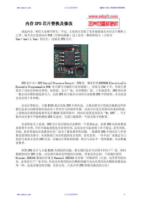
内存SPD芯片替换及修改说起内存,相信大家都不陌生。
不过,大家的目光除了更多地投放在内存芯片颗粒上之外,很少会注意到内存PCB(印刷电路板)边上还有一颗体积较小(大约为3mm×4mm×1.5mm)的芯片,这就是SPD芯片.SPD是什么?SPD(Serial Presence Detect): SPD是一颗8针的EEPROM(Electrically Erasable Programmable ROM 电可擦写可编程只读存储器), 容量为256字节,里面主要保存了该内存的相关资料,如容量、芯片厂商、内存模组厂商、工作速度等。
SPD的内容一般由内存模组制造商写入。
支持SPD的主板在启动时自动检测SPD中的资料,并以此设定内存的工作参数。
启动计算机后,主板BIOS就会读取SPD中的信息,主板北桥芯片组就会根据这些参数信息来自动配置相应的内存工作时序与控制寄存器,从而可以充分发挥内存条的性能。
上述情况实现的前提条件是在BIOS设置界面中,将内存设置选项设为“By SPD”。
当主板从内存条中不能检测到SPD信息时,它就只能提供一个较为保守的配置。
从某种意义上来说,SPD芯片是识别内存品牌的一个重要标志。
如果SPD内的参数值设置得不合理,不但不能起到优化内存的作用,反而还会引起系统工作不稳定,甚至死机。
因此,很多普通内存或兼容内存厂商为了避免兼容性问题,一般都将SPD中的内存工作参数设置得较为保守,从而限制了内存性能的充分发挥。
更有甚者,一些不法厂商通过专门的读写设备去更改SPD信息,以骗过计算机的检测,得出与实际不一致的数据,从而欺骗消费者。
即然SPD芯片与主板BIOS有相似的功能,那么我们是否可以将不同生产厂家,相同数据的内存SPD互换,以达到升级内存性能的目的呢。
答案是肯定的,下面我们使用Hyundai DDR266散装内存条及Ramaxel DDR266内存做一详细说明(注意:这里所用的内存,必须是生产厂家不同,但是内存使用的内存颗粒的编号及内存使用内存颗粒的数量必须一样,这也是修改的关键;在此文内,只是介绍SPD替换及修改的方法)即然要对SPD芯片进行读写,因此就要用到编程器;而且由于SPD芯片是焊接在内存电路板上的。
- 1、下载文档前请自行甄别文档内容的完整性,平台不提供额外的编辑、内容补充、找答案等附加服务。
- 2、"仅部分预览"的文档,不可在线预览部分如存在完整性等问题,可反馈申请退款(可完整预览的文档不适用该条件!)。
- 3、如文档侵犯您的权益,请联系客服反馈,我们会尽快为您处理(人工客服工作时间:9:00-18:30)。
3,4
5,4,3
6,5,4 X =< 3.80 SODIMM
5,4,3
38h
70h 01h 04h 00h 07h
38h
Analysis probe not installed, FET switch external not enable Supports weak driver, 50Ohm ODT, PASR 3.75ns +/-0.5ns 5.0ns +/-0.6ns 12.5ns 3.0ns +/- 0.45ns 3.75ns +/-0.5ns 15ns 7.5ns 12.5ns 15ns 45ns 1GB 0.175ns 0.25ns 0.05ns 0.125ns 0.20ns 0.27ns 0.10ns 0.17ns 15ns 0.22ns 0.25ns 0.37ns 0.35ns 0.47ns 0.15ns 0.27ns 17h 25h 05h 12h 40ns 32h 3.75ns +/-0.5ns 5.0ns +/-0.6ns 5.0ns +/-0.6ns 3Dh 50h 50h 60h 32h 3Dh 50h 30h 45h
Function described
Internal write to read command delay(=tWTR) Internal read to precharge command delay(=tRTP) Memory analysis probe characteristics Extension of Byte41 tRC and Byte42 tRFC DDR2 SDRAM device min. active to active/auto refresh time(=tRC) DDR2 SDRAM device min. auto-refresh to active/auto-refresh command period(=tRFC) DDR2 SDRAM device max. device cycle time(=tCK max) DDR2 SDRAM device max. skew for DQS and associated DQ signals(=tDQSQ max) DDR2 SDRAM read data hold skew factor(=tQHS) PLL Relock Time DT in SPD High Temp. Self Refresh IDD in SPD SPD data revision code Checksum for Bytes 0 ~ 62 Manufacturer JEDEC ID code ......Manufacturer JEDEC ID code Manufacturing location Manufacturer Part #(Memory module) Manufacturer part # (DIMM configuration) Manufacturer part # (Data bits & Module type) ......Manufacturer part # (Data bits & Module type) ......Manufacturer part # (Data bits & Module type) Manufacturer part # (Operating Voltage) Manufacturer part # (Module depth) Manufacturer part # (Module depth) Manufacturer Part # (Refresh. # of rows in comp. & interface) Manufacturer part # (composition component) Manufacturer part # (Component revision) Manufacturer part # (Package type) Manufacturer part # (PCB revision) Manufacturer part # (Hyphen) Manufacturer part # (Power) Manufacturer part # (Minimum cycle time) Manufacturer part # (Minimum cycle time) Manufacturer part # (T.B.D) Manufacturer Revision Code(For PCB) Manufacturer Revision Code (For component) Manufacturing Date (Year) Manufacturing date (week) Assembly serial # Manufacturer specific data(may be used in future) Open for customer use 1 . This will typically be programmed as 128 Bytes. 2 . This will typically be programmed as 256 Bytes. 3 . From Datasheet
Hex Value CCC CE7 CF7 CE6
80h 08h 08h 0Eh 0Ah 61h 40h 00h 05h 30h 45h 00h 82h 08h 00h 00h 0Ch 08h 3Dh 50h 50h 60h
CD5
CD5
CCC
Note
1 2
+/-0.45ns +/-0.5ns Non parity/ECC 7.8us x8 N/A 4,8 8 banks
SERIAL PRESENCE DETECT
M470T5663QZ3-CE7/CF7/CE6/CD5/CCC
Organization :256M x 64 Composition :128M x 8 * 16ea Used component part # :K4T1G084QQ-HCE7/F7/E6/D5/CC # of rows in module Row :2 # of banks in component :8 banks Feature :30mm height & double sided component Refresh :8K/64ms Bin Sort : E7(DDR2-800@CL=5), F7(DDR2-800@CL=6), E6(DDR2-667@CL=5), D5(DDR2-533@CL=4), CC(DDR2-400@CL=3) Contents :
Byte #
0 1 2 3 4 5 6 7 8 9 10 11 12 13 14 15 16 17 18 19 20 21 22 23 24 25 26 27 28 29 30 31 32 33 34 35 36
Function described
# of Serial PD Bytes written during module production Total Number of SPD memory device Fundameatal memory type # of row address on this assembly # of column address on this assembly # of module rows on this assembly Data width of this assembly Reserved Voltage interface level of this assembly DDR2 SDRAM cycle time at Max. Supported CAS latency=X DDR2 SDRAM Access time from clock at CL=X DIMM configuration type (address&command parity, data parity, ECC) Refresh rate Primary DDR2 SDRAM width Error checking DDR2 SDRAM data width Reserved DDR2 SDRAM device attributes : Burst lengths supported DDR2 SDRAM device attributes : # of banks on each DDR2 SDRAM device DDR2 SDRAM device attributes : CAS latency supported DIMM Mechanical Characteristics DIMM type information DDR2 SDRAM module attributes DDR2 SDRAM device attributes : General DDR2 SDRAM cycle time at CL= X-1 DDR2 SDRAM access time from clock at CL= X-1 DDR2 SDRAM cycle time at CL= X-2 DDR2 SDRAM access time from clock at CL= X-2 Minimum row precharge time(=tRP) Minimum row active to row active delay(=tRRD) Minimum RAS to CAS delay(=tRCD) Minimum active precharge time(=tRAS) Module rank density Command and address setup time before clock(=tIS) Command and address hold time after clock(=tIH) Data input setup time before strobe(=tDS) Data input hold time after strobe(=tDH) Write recovery time(=tWR)