正常来水年(90%保证率)水量分配表【模板】
CB-C8VM资料
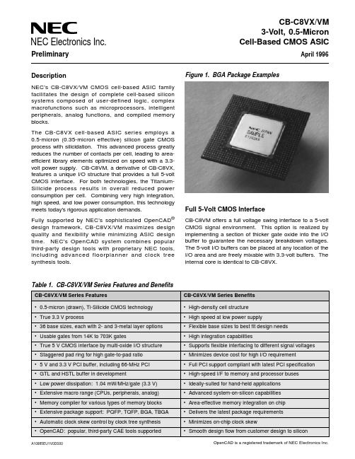
NEC Electronics Inc.CB-C8VX/VM 3-Volt, 0.5-Micron Cell-Based CMOS ASICDescriptionNEC's CB-C8VX/VM CMOS cell-based ASIC family facilitates the design of complete cell-based silicon systems composed of user-defined logic, complex macrofunctions such as microprocessors, intelligent peripherals, analog functions, and compiled memory blocks.The CB-C8VX cell-based ASIC series employs a 0.5-micron (0.35-micron effective) silicon gate CMOS process with silicidation. This advanced process greatly reduces the number of contacts per cell, leading to area-efficient library elements optimized on speed with a 3.3-volt power supply. CB-C8VM, a derivative of CB-C8VX,features a unique I/O structure that provides a full 5-volt CMOS interface. For both technologies, the Titanium-Silicide process results in overall reduced power consumption per cell. Combining very high integration,high speed, and low power consumption, this technology meets today's rigorous application demands.Fully supported by NEC's sophisticated OpenCAD ®design framework, CB-C8VX/VM maximizes design quality and flexibility while minimizing ASIC design time. NEC's OpenCAD system combines popular third-party design tools with proprietary NEC tools,including advanced floorplanner and clock tree synthesis tools.A10985EU1V0DS00April 1996Table 1. CB-C8VX/VM Series Features and BenefitsFigure 1.BGA Package ExamplesOpenCAD is a registered trademark of NEC Electronics Inc.PreliminaryFull 5-Volt CMOS InterfaceCB-C8VM offers a full voltage swing interface to a 5-volt CMOS signal environment. This option is realized by implementing a section of thicker gate oxide into the I/O buffer to guarantee the necessary breakdown voltages.The 5-volt I/O buffers can be placed at any location of the I/O area and are freely mixable with 3.3-volt buffers. The internal core is identical to CB-C8VX.CB-C8VX/VM25-Volt-Tolerant InterfaceCB-C8VX supports both 3.3-volt and 5-volt-tolerant signaling. The 5-volt-tolerant buffers enable CB-C8VX devices to communicate with 5-volt TTL signals while protecting the ASIC. CB-C8VX requires only a 3.3-volt power supply.Integration and PerformanceGate complexities up to 703K usable gates can be integrated on the largest of 36 die sizes, each routable with 2- or 3-metal layers. This gives enough flexibility to optimally fit design needs. Twenty-two die sizes offer a single I/O pad ring and 14 are equipped with a staggered dual pad ring in order to achieve a high pad-to-gate ratio. For details, please refer to Table 2 and Table 3.The family offers an extensive library of primitive macrofunctions characterized for 3.3-volt operation.Each of these blocks has several different drive strengths, allowing the synthesis tool to select the most suitable block for the required internal load. This generally reduces the design overhead without influencing design performance. The internal gate delay for a two-input NAND gate is 110 picoseconds (ps), (F/O=1, L=0mm) and 220 ps under loaded conditions (F/O=2, L=2mm).To meet today's high-speed demands, high-perform-ance I/O macros are mandatory. CB-C8VX/VM supports macros such as GTL and HSTL for fast, low-power data transfer, PLLs to synchronize on-chip system clocks, and PCI signaling standards. Also,CB-C8VX/VM offers a variety of macrofunctions to be incorporated on a single chip. These macrofunctions include CPU cores, peripheral devices, RAM/ROM and analog functions, enabling designers to create systems on silicon.Low Power ConsumptionNEC's CB-C8VX/VM Ti-Silicide process featuresexceptionally low power dissipation to facilitate high-speed operation without the need of costly package options, and drastically increases battery life for hand-held applications. At 3.3-volts, power dissipation for internal cells is 1.04 µW/gate/MHz.Table 2. CB-C8VX/VM Die Steps (124µ pad pitch)Step I/O Max. Usable Gates (1)2 Layer 3 Layer B18881307819617B571041879728195B971202543838156C371363321949828C761524201663023D161685170377555D551846254793820D7519267969101953E1520880484120727E5422493875140813E94240106000159000F34256120969181453F74272136641204961G14288153500230250G53304171234256852G93320183078274617H33336202328303492H72352222219333328J32376254094381141J71392275813413719K11408298797448195K90440347031520547Single pad ring die steps.(1) Glue logic only, with average utilization.Table 3. CB-C8VX/VM Die StepsStep I/O Max. Usable Gates (1)2 Layer 3 Layer B73T 1481884428266C37T 1883025045375C50T 1963270349055D01T 2284400066000D52T 2605704785570D90T 28467797101695E54T 32488281132422F18T 364109125163688F70T 396128875193313G34T 436155297232945H49T 508202766304148J51T 572256047384070K92T 660337531506297M97T788468984703477Dual pad ring die steps.(1) Glue logic only, with average utilization.(80µ staggered pad pitch)3CB-C8VX/VMMulti-Voltage I/O InterfaceFor those systems not yet ready to migrate completely to 3.3-volts, CB-C8 has a full 5-volt CMOS interface available. Applying two additional process steps that realize a "multi-oxide" section in the I/O area, 5-volt speed and drive capabilities are available with the help of a separate 5-volt supply rail. The 5-volt I/O buffers include level shifters to convert the 5-volt signal levels to the internal core supply voltage of 3.3-volts. This CB-C8 derivative is called CB-C8VM and is, except for the different I/O structure, identical to CB-C8VX.For moderate speed and driveable 5-volt I/O cell requirements, CB-C8VM's flexibility provides tolerant I/Os that safely interface to 5V devices using a single 3.3-volt power supply.In both cases, the 3.3-volt and 5-volt interfaces can be mixed without restriction along the entire I/O ring.System on SiliconNEC offers a wide selection of CPU/MCU cores, industry-standard intelligent peripheral macros, and compilable RAM/ROM blocks as well as analog functions in hard macro form that can be integrated onto a single CB-C8VX/VM chip. Including such macrofunctions in an ASIC design makes it possible to achieve a high level of integration, performance, and system security.The range of NEC's on-chip macrofunctions includes NEC's proprietary 32-bit V810™ RISC CPU, and an upgraded high-speed version of the popular 16-bit CPU V30HL™, called V30MX™, which operates at clock speeds of 33 MHz at 3.3-volts, and offers an improved 286-compatible address pipelining and uses a 24-bit address bus. Other specific cores can be implemented on request. For details about the full range of on-chip macrofunctions, refer to Table 4.Embedded macrofunctions are easy to place, route,and simulate. Because these macros are derived from NEC's standard parts, they have fully characterized parameters and can be tested with standard test vectors to ensure full functionality and reliability.NEC's test bus architecture allows complete system simulation, production testing of the internal circuits of the macrofunctions, and seamless embedded CPU core emulation. The CPU may be connected externally and can be replaced by an in-circuit emulator (ICE). All this is performed with only two dedicated test control pins.CB-C8VXCB-C8VM Device Names µPD97xxx µPD99xxx Interface options• true 3.3 V • true 3.3 V • 5 V tolerant• 5 V tolerant • true 5 V CMOSCore voltage 3.3 V 3.3 V I/O voltage3.3 V3.3 V and 5 VTable 4. Macrofunction RangeComparable Macro Device DescriptionNZ 70008H µPD70008A Z80™: 8-bit microprocessor (16 MHz)NZ V30MX µPD70108H V30MX: 16-bit microprocessor (16-bit data bus, 33 MHz)NZ V810µPD70732V810™: 32-bit RISC microprocessor (25 MHz)NZ 71037H µPD71037Programmable DMA controller (4 channels, 20 MHz)NZ 71051H µPD71051USART: serial data control (full-duplex Tx/Rx, 300kbit/s, 20 MHz)NZ 71054H µPD71054Programmable timer/counter (16-bit, 3 counter, 6 modes, 20 MHz)NZ 71055H µPD71055Programmable parallel interface (8-bit, 3 I/O ports, 3 modes)NZ 71059H µPD71059Programmable interrupt control (64 interrupt request inputs)NA 4993µPD49938-bit parallel I/O real-time clockNA 72065BL µPD72065B Single-double density floppy disk controllerNZ 72103µPD72103HDLC Controller: Full duplex, Baud rate 4 Mbps, built-in DMA M I 2C™—I 2C Bus interface: receive, transmit, master and slave NA 16450L NS16C450UART: for PC-compatible serial portsNA 16550LNS16550AUART with FIFO: for PC-compatible serial portsZ80 is a trademark of Zilog, Inc.V30HL, V30MX and v810 are trademarks of NEC Corporation I 2C is a trademark of PhilipsCB-C8VX/VM4Memory MacrosAll memory blocks in NEC's CB-C8VX/VM technology are realized as embedded hard macros and are generated by a memory compiler. To ease the task of RAM testing for the designer, NEC supplies standard test pattern sets, which help to save valuable develop-ment time. NEC offers seven different types of memory blocks, as shown in Table 5.PackagingNEC offers a wide variety of over 60 package types.The CB-C8VX/VM family can be packaged in NEC's most popular surface-mount and through-hole packages. These include plastic quad-flat packs (PQFPs) with up to 376 pins. The QFP range includes thin packages (TQFP, LQFP), QFPs with integrated heatspreader, and tape-automated-bonding QFPs (TAB-QFP) with up to 304 pins. Pin grid arrays (PGAs) with up to 528 pins, BGA packages with up to 672 pins, and TBGA packages with up to 696 pins can be used.CB-C8VX/VM ApplicationsCB-C8VX/VM devices are targeted for 3.3-volt products in telecommunications, electronic data processing (EDP), and consumer applications. Typical telecommunications applications include cellular telephones, high-end pagers, and PCMCIA devices, as well as broad-band communication systems up to 156Mbit/s. In the EDP segment, applications range from personal computers to high-end workstations andTable 5. Memory BlocksMacro TypeWord Range Bit Range Step (Word / Bit)ROM128 - 8192 4 - 64128 / 2256 - 16384 2 - 32256 / 1512 - 32768 1 - 16512 / 1Low-power RAM, single-port64 - 512 1 - 3216 / 1(asynchronous, bi-directional I/O)128 - 1024 1 - 1632 / 1256 - 2048 1 - 864 / 1Low-power RAM, single-port 64 - 512 1 - 3216 / 1(synchronous, separate I/O)128 - 1024 1 - 1632 / 1256 - 2048 1 - 864 / 1High-density RAM, single-port 128 - 2048 1 - 6416 / 1(synchronous, separate I/O)High-speed RAM, single-port 32 - 20481- 3232 / 1(synchronous, separate I/O)Register files, dual-port 8 - 256 4 - 32 4 / 1Register files, triple-port8 - 2564 - 324 / 1mainframes, multimedia platforms, graphic accel-erators, personal digital assistants (PDAs), notebook and pen-based devices, hand-held data terminals, and hard disk controllers. Consumer applications include games, video cameras, portable printers, and sophisticated calculators.Each of these applications demands the benefits of increased integration and low power consumption that only a cell-based family using an optimized 3.3-volt process technology can deliver. CB-C8VX/VM provides the flexibility needed when a 3.3-volt process is required.Design Tool SupportThe CB-C8VX/VM family is fully supported by NEC's OpenCAD Design System, a unified front-to-back-end design package that allows designers to mix and match tools from the industry's most popular third-party vendors and from NEC's offering of powerful propri-etary software tools. These tools perform schematic capture, logic synthesis, floorplanning, logic and timing simulation, layout, design and circuit rule check, and memory compilations.The company's proprietary clock tree synthesis tool automatically buffers clock lines as needed to minimize clock skew, which is essential for half-micron designs.The nonlinear delay calculator ensures timing accuracy throughout the simulation, synthesis, and silicon stages.Finally, NEC's memory compiler software enables memory block generation based on size and perform-ance requirements.5CB-C8VX/VMInput/Output Capacitance (V DD =V I =0 V; f =1 MHz)TerminalSymbol Typ Max Unit Input C IN 1020pF Output C OUT 1020pF I/OC I/O1020pF(1)Values include package pin capacitanceAbsolute Maximum RatingsPower supply voltage, V DD 3.3 V supply –0.5 to +4.6 V 5 V supply –0.5 to +6.0 VI/O voltage, V I /V O 3.3 V interface block –0.5 to +4.6 V and (V I /V O < V DD +0.5 V) 5 V-tolerant block –0.5 to +6.6 V and (V I /V O < V DD +3.0 V) 5 V swing block –0.5 to +6.0 V and (V I /V O < V DD +0.5 V)Latch-up current, I LATCH >1 A (typ)Operating temperature, T OPT –40 to +85°C Storage temperature, T STG–65 to +150°CAC Characteristics (V DD = 3.3 V ± 0.3 V; T J = –40 to +125°C)Parameter Symbol MinTyp MaxUnit Conditions Toggle frequency f TOG480MHzD-F/F; F/O = 2 mmDelay time2-input NAND (F322)t PD 236ps F/O = 1; L = 0 mm t PD 272ps F/O = 2; L = typ Flip-flop (F661)t PD 777ps F/O = 1; L = 0 mm t PD 865ps F/O = 2; L = typ t SETUP 420ps —t HOLD 580ps —Input buffer (FI01)t PD 126ps F/O = 1; L = 0 mm t PD 228ps F/O = 2; L = typ Output buffer (9 mA) 3.3 V t PD 1.24ns C L = 15 pF Output buffer (9 mA) 5 V-tolerant t PD 4.262ns C L = 15 pF Output buffer (6 mA) 5 V-swing t PD 2.698ns C L = 15 pF Output rise time (9 mA)t R 1.88ns C L = 15 pF Output fall time (9 mA)t F1.32nsC L = 15 pFRecommended Operating Conditions (V DD = 3.3 V ± 0.165 V; V CC = 5.0 V ± 0.5 V; T J = –40 to +125°C)3.3 V Interface5 V Tolerant5 V Swing 5 V Swing BlockBlockCMOS Level TTL Level (CB-C8VX/VM)(CB-C8VM)(CB-C8 VM)ParameterSymbol Min Max Min Max Min Max Min Max Unit I/O power supply voltage V DD 3.0 3.6 3.0 3.6 4.5 5.5 4.75 5.25V Junction temperature T J –40+125–40+125–40+125–40+125°C High-level input voltage V IH 2.0V DD 2.0 5.50.7 V DDV DD 2.0V DD V Low-level input voltage V IL 00.800.800.3 V DD 00.8V Positive trigger voltage V P 1.2 2.4 1.2 2.4 1.8 4.0 1.2 2.4V Negative trigger voltage V N 0.6 1.80.6 1.80.6 3.10.6 1.8V Hysteresis voltage V H 0.3 1.50.3 1.50.3 1.50.3 1.5V Input rise/fall time t R , t F 0200020002000200ns Input rise/fall time, Schmittt R , t F10101010msPower ConsumptionDescription Limits Unit Internal gate (1) 1.04µW/MHz Input block —µW/MHz Output block—µW/MHz(1)Assumes 30% internal gate switching at one timeCaution: Exposure to absolute maximum ratings for extended periods may affect device reliability; exceeding the ratings could cause permanent damage. The device should not be operated outside the recommended operating conditions.Caution: Exposure to absolute maximum ratings for extended periods may affect device reliability; exceeding the ratings could cause permanent damage. The device should not be operated outside the recommended operating conditions.CB-C8VX/VM6DC Characteristics (V DD = 3.3 V ± 0.3 V, 5 V ± 0.5 V; T A = –40 to +125°C)ParametersSymbol Conditions MIN.TYP.MAX.Unit Static current consumptionI L V I = V DD B18 to H33200µA or GNDH72 to K90300µA Off-state output current I OZ V O = V DD or GND ±10µA Output short-circuit current I OS V O = 0V–250mAInput leakage currentI INormal inputV I = V DD or GND ±10-5±10µA With pull-up resistor (50 ký)V I = GND –10–40–80µA With pull-up resistor (5 ký)V I = GND –130–350–640µA With pull-down resistor (50 ký)V I = V DD1065130µALow-level output currentI OL3 V interface bufferV OL = 0.4VmA 3 mA I OL 3mA 6 mA I OL 6mA 9 mA I OL 9mA 12 mA I OL 12mA 18 mA I OL 18mA 24 mA I OL24mA 5 V-tolerant bufferV OL = 0.4VmA 1 mA I OL 1mA 2 mA I OL 2mA 3 mA I OL 3mA 6 mA I OL 6mA 9 mA I OL9mA 5 V swing bufferV OL = 0.4VmA 1 mA I OL 1mA 2 mA I OL 2mA 3 mA I OL 3mA 6 mA I OL 6mA 9 mA I OL 9mA 12 mA I OL 12mA 18 mAI OL 18mAHigh-level output currentI OH3 V interface bufferV OH = 2.4V3 mA I OH -3mA 6 mA I OH -6mA 9 mA I OH -9mA 12 mA I OH -12mA 18 mA I OH -18mA 24 mAI OH-24mACB-C8VX/VM DC Characteristics (continued) (V= 3.3 V ± 0.3 V, 5 V ± 0.5 V; T A= –40 to +125°C)DDParameters Symbol Conditions MIN.TYP.MAX.Unit High-level output current I OH5 V-tolerant buffer V OH = 2.4 V1 mA I OH–1mA2 mA I OH–2mA3 mA I OH–3mA6 mA I OH–6mA9 mA I OH–9mA5 V swing buffer V OH = –0.4 V1 mA I OH–1mA2 mA I OH–2mA3 mA I OH–3mA6 mA I OH–6mA9 mA I OH–9mA12 mA I OH–12mA18 mA I OH–18mA Low-level output voltage V OL I OL = 0 mA0.1V3 V interface buffer V OL0.1V5 V interface buffer V OL0.1V5 V swing buffer V OL0.1VHigh-level output voltage V OH I OH = 0 mA V3 V interface buffer V OH V DD–0.1V5 V interface buffer V OH V DD–0.2V5 V swing buffer V OH V DD–0.1V78For literature, call toll-free 7 a.m. to 6 p.m. Pacific time: 1-800-366-9782or FAX your request to: 1-800-729-9288No part of this document may be copied or reproduced in any form or by any means without the prior written consent of NEC Electronics Inc.(NECEL). The information in this document is subject to change without notice. ALL DEVICES SOLD BY NECEL ARE COVERED BY THE PROVISIONS APPEARING IN NECEL TERMS AND CONDITIONS OF SALES ONLY. INCLUDING THE LIMITATION OF LIABILITY, WAR-RANTY, AND PATENT PROVISIONS. NECEL makes no warranty, express, statutory, implied or by description, regarding information set forth herein or regarding the freedom of the described devices from patent infringement. NECEL assumes no responsibility for any errors that may appear in this document. NECEL makes no commitments to update or to keep current information contained in this document. The devices listed in this document are not suitable for use in applications such as, but not limited to, aircraft control systems, aerospace equipment, submarine cables, nuclear reactor control systems and life support systems. “Standard” quality grade devices are recom-mended for computers, office equipment, communication equipment, test and measurement equipment, machine tools, industrial robots,audio and visual equipment, and other consumer products. For automotive and transportation equipment, traffic control systems, anti-disaster and anti-crime systems, it is recommended that the customer contact the responsible NECEL salesperson to determine the reliabilty requirements for any such application and any cost adder. NECEL does not recommend or approve use of any of its products in life support devices or systems or in any application where failure could result in injury or death. If customers wish to use NECEL devices in applications not intended by NECEL, customer must contact the responsible NECEL sales people to determine NECEL’s willingness to support a given application.©1996 NEC Electronics Inc./Printed in U.S.A.Document No. A10985EU1V0DS00NEC ASIC DESIGN CENTERSWEST•3033 Scott Boulevard Santa Clara, CA 95054TEL 408-588-5008FAX 408-588-5017•One Embassy Centre9020 S.W. Washington Square Road,Suite 400Tigard, OR 97223TEL 503-671-0177FAX 503-643-5911THIRD-PARTY DESIGN CENTERSSOUTH CENTRAL/SOUTHEAST•Koos Technical Services, Inc.385 Commerce Way, Suite 101Longwood, FL 32750TEL 407-260-8727FAX 407-260-6227•Integrated Silicon Systems Inc.2222 Chapel Hill Nelson Highway Durham, NC 27713TEL 919-361-5814FAX 919-361-2019•Applied Systems, Inc.1761 W. Hillsboro Blvd., Suite 328Deerfield Beach, FL 33442TEL 305-428-0534FAX 305-428-5906NORTH CENTRAL/NORTHEAST•The Meadows, 2nd Floor 161 Worcester Road Framingham, MA 01701TEL 508-935-2200FAX 508-935-2234•Greenspoint Tower2800 W. Higgins Road, Suite 765Hoffman Estates, IL 60195TEL 708-519-3945FAX 708-882-7564NEC Electronics Inc.CORPORATE HEADQUARTERS2880 Scott Boulevard P.O. Box 58062Santa Clara, CA 95052TEL 408-588-6000SOUTH CENTRAL/SOUTHEAST•16475 Dallas Parkway, Suite 380Dallas, TX 75248TEL 972-735-7444FAX 972-931-8680•Research Triangle Park2000 Regency Parkway, Suite 455Cary, NC 27511TEL 919-460-1890FAX 919-469-5926•Two Chasewood Park 20405 SH 249, Suite 580Houston, TX 77070TEL 713-320-0524FAX 713-320-0574。
半导体FAB里基本的常识简介

CVD晶圆制造厂非常昂贵的原因之一,是需要一个无尘室,为何需要无尘室答:由于微小的粒子就能引起电子组件与电路的缺陷何谓半导体?答:沉积介电质层及金属层何谓CVD(ChemicalVaporDep.)答:CVD是一种利用气态的化学源材料在晶圆表面产生化学沉积的制程CVD分那几种?答:PE-CVD(电浆增强型)及Thermal-CVD(热耦式) 为什幺要用铝铜(AlCu)合金作导线?答:良好的导体仅次于铜介电材料的作用为何?答:做为金属层之间的隔离答:掺杂硼磷的硅玻璃(Borophosphosilicateglass) 何谓TEOS?答:Tetraethoxysilane用途为沉积二氧化硅TEOS在常温时是以何种形态存在?答:液体二氧化硅其K值为3.9表示何义答:表示二氧化硅的介电质常数为真空的3.9倍氟在CVD的工艺上,有何应用答:作为清洁反应室(Chamber)用之化学气体更换过任何气体管路上的零件之后,一定要做何动作? 答:用氦气测漏机来做测漏维修尚未降至室温之反应室(Chamber),应配带何种手套答:石棉材质之防热手套并宜在80摄式度下始可动作何为真空(Vacuum)?半导体业常用真空单位是什幺?答:半导体业通常用Torr作为真空的压力单位,一大气压相当760Torr,低于760Torr压力的环境称为真空.真空Pump的作用?答:降低反应室(Chamber)内的气体密度和压力ETCH何谓蚀刻(Etch)?答:将形成在晶圆表面上的薄膜全部,或特定处所去除至必要厚度的制程。
蚀刻种类:答:(1)干蚀刻(2)湿蚀刻蚀刻对象依薄膜种类可分为:答:poly,oxide,metal半导体中一般金属导线材质为何?答:鵭线(W)/铝线(Al)/铜线(Cu)何谓干式蚀刻?答:利用plasma将不要的薄膜去除何谓Under-etching(蚀刻不足)?答:系指被蚀刻材料,在被蚀刻途中停止造成应被去除的薄膜仍有残留何谓Over-etching(过蚀刻)答:蚀刻过多造成底层被破坏何谓Etchrate(蚀刻速率)答:单位时间内可去除的蚀刻材料厚度或深度何谓Seasoning(陈化处理)答:利用离心力将晶圆表面的水份去除何谓MaragoniDryer答:利用表面张力将晶圆表面的水份去除何谓IPAVaporDryer答:利用IPA(异丙醇)和水共溶原理将晶圆表面的水份去除测Particle时,使用何种测量仪器?答:TencorSurfscan测蚀刻速率时,使用何者量测仪器?答:膜厚计,测量膜厚差值答:因为金属线会溶于硫酸中"HotPlate"机台是什幺用途?答:烘烤HotPlate烘烤温度为何?答:90~120度C何种气体为PolyETCH主要使用气体?答:Cl2,HBr,HCl用于Al金属蚀刻的主要气体为答:Cl2,BCl3答:利用UV光对光阻进行预处理以加强光阻的强度"UVcuring"用于何种层次?答:金属层何谓EMO?答:机台紧急开关EMO作用为何?答:当机台有危险发生之顾虑或已不可控制,可紧急按下湿式蚀刻门上贴有那些警示标示?答:(1)警告.内部有严重危险.严禁打开此门(2)机械手臂危险.严禁打开此门(3)化学药剂危险.有毒气体之阀柜(VMB)功用为何?答:当有毒气体外泄时可利用抽气装置抽走,并防止有毒气体漏出电浆的频率一般13.56MHz,为何不用其它频率?答:为避免影响通讯品质,目前只开放特定频率,作为产生电浆之用,如380~420KHz,13.56MHz,2.54GHz等何谓ESC(electricalstaticchuck)答:利用静电吸附的原理,将Wafer固定在极板(Substrate)上Asher主要气体为答:O2Asher机台进行蚀刻最关键之参数为何?简述EPD之功用答:侦测蚀刻终点;Endpointdetector利用波长侦测蚀刻终点何谓MFC?答:massflowcontroler气体流量控制器;用于控制反应气体的流量GDP为何?答:气体分配盘(gasdistributionplate)GDP有何作用?答:均匀地将气体分布于芯片上方何谓isotropicetch?简述何谓田口式实验计划法?答:利用混合变因安排辅以统计归纳分析何谓反射功率?答:蚀刻过程中,所施予之功率并不会完全地被反应腔内接收端所接受,会有部份值反射掉,此反射之量,称为反射功率LoadLock之功能为何?答:Wafers经由loadlock后再进出反应腔,确保反应腔维持在真空下不受粉尘及湿度的影响.厂务供气系统中何谓BulkGas?答:BulkGas为大气中普遍存在之制程气体,如N2,O2,Ar等.答:利用水循环将废气溶解之后排放至废酸槽何谓RPM?答:即RemotePowerModule,系统总电源箱.火灾异常处理程序答:(1)立即警告周围人员.(2)尝试3秒钟灭火.(3)按下EMO停止机台.(4)关闭VMBValve并通知厂务.(5)撤离.一氧化碳(CO)侦测器警报异常处理程序答:(1)警告周围人员.(2)按Pause键,暂止Run货.(3)立即关闭VMB阀,并通知厂务.(4)进行测漏.何谓WAC(WaferlessAutoClean)答:无wafer自动干蚀刻清机何谓DryClean答:干蚀刻清机日常测机量测etchrate之目的何在?答:因为要蚀刻到多少厚度的film,其中一个重要参数就是蚀刻率操作酸碱溶液时,应如何做好安全措施?答:(1)穿戴防酸碱手套围裙安全眼镜或护目镜(2)操作区备有清水与水管以备不时之需(3)操作区备有吸酸棉及隔离带答:将wafer传进chamber与传出chamber之用何谓MTBC?(meantimebetweenclean)答:上一次wetclean到这次wetclean所经过的时间RFGenerator是否需要定期检验?答:是需要定期校验;若未校正功率有可能会变化;如此将影响电浆的组成为何需要对etchchamber温度做监控?答:因为温度会影响制程条件;如etchingrate/均匀度为何需要注意drypumpexhaustpresure(pump出口端的气压)?答:因为气压若太大会造成pump负荷过大;造成pump跳掉,影响chamber的压力,直接影响答:208V三相干式蚀刻机台分为那几个部份?答:(1)Load/Unload端(2)transfermodule(3)Chamberprocessmodule(4)真空系统(5)GASsystem(6)RFsystemPHOTO答:当供电局供电中断时,本厂因有紧急发电机设备,配合各相关监视系统,仍然能保持FAB之Safety,所以人员仍可安心待在FAB中.化剂,可将有机物氧化分解为CO2+H2O,因此在IC制程中常用来去除残留之光阻,另外对金属污染及微尘污染也有相当好的清洗效果。
JUMO 温度传感器说明书

Page 1/11Data Sheet 702040Blocks tructureFeature sk S tructured operating and programming layout k S elf-optimi s ation k Ramp functionk Timer functionk Digital input filter withprogrammable filter time con s tant k 1 limit comparator k limit s witchJUMO iTRON 04/08/16/32Compact microproce ss or controller sHou s ing for flu s h-panel mounting to DIN IEC 61554Brief de s criptionThe JUMO iTRON controller s erie s compri s e s univer s al and freely programmable com-pact in s trument s for a variety of control ta sks . It con s i s t s of five model s , with the bezel s ize s 96mm x 96mm, 96mm x 48mm in portrait and land s cape format, 48mm x 48mm and 48mm x 24mm.The controller s feature a clearly readable 7-s egment di s play which, depending on the ver-s ion, i s 10 or 20 mm high, for proce ss value and s etpoint indication or for dialog s . Only three k ey s are needed for configuration. Parameter s etting i s arranged dynamically, and after two operation-free s econd s the value i s accepted automatically. S elf-optimi s ation,which i s provided a s s tandard, e s tabli s he s the optimum controller parameter s by a k ey s tro k e. The ba s ic ver s ion al s o include s a ramp function with adju s table gradient s . A timer function ha s been integrated a s an extra.All controller s can be employed a s s ingle-s etpoint controller s with a limit comparator, or as double-s etpoint controller s . The lineari s ation s of the u s ual tran s ducer s are stored. Pro-tection i s IP66 at the front and IP20 at the bac k . The electrical connection i s by a plug-in connector with s crew terminal s .The input s and output s are s hown in the bloc k s tructure below.JUMO iTRON 08Type 702042JUMO iTRON 04Type 702044JUMO iTRON 08Type 702043JUMO iTRON 32Type 702040JUMO iTRON 16Type 702041Approval s /approval mark s (s ee "Technical data")Data Sheet 702040Page 2/11Technical dataThermocouple inputRe s i s tance thermometer inputStandard s ignal inputMea s urement circuit monitoring 1De s ignation Range 1Mea s urement accuracy Ambienttemperature error Fe-Con L Fe-Con J EN 60584Cu-Con U Cu-Con T EN 60584NiCr-Ni K EN 60584NiCr S i-Ni S i N EN 60584Pt10Rh-Pt S EN 60584Pt13Rh-Pt R EN 60584Pt30Rh-Pt6Rh BEN 60584-200to +900°C -200to +1200°C -200to +600°C -200to +400°C -200to +1372°C -100to +1300°C0— 1768°C 0—1768°C +300— 1820°C≤0.4%≤0.4%≤0.4%≤0.4%≤0.4%≤0.4%≤0.4%≤0.4%≤0.4%100 ppm/°C 100 ppm/°C 100 ppm/°C 100 ppm/°C 100 ppm/°C 100 ppm/°C 100 ppm/°C 100 ppm/°C 100 ppm/°CCold junctionPt 100 internal1. The s e range s refer to the ambient temperature of 20°CDe s ignation Connection type RangeMea s urement accuracy Ambienttemperature error Pt 100 EN 607512-/3-wire -200to +850°C ≤0.1%50 ppm/°C Pt 1000 EN 607512-/3-wire -200to +850°C ≤0.1%50 ppm/°C K TY11-62-wire-50to +150°C≤1.0%50 ppm/°CS en s or lead re s i s tance 20Ω max. per lead for 2- and 3-wire circuitMea s urement current 250µALead compen s ationNot required for 3-wire circuit. For 2-wire circuit, lead compen s ation can be implemented in s oftware through proce ss value correction.De s ignation RangeMea s urement accuracy Ambienttemperature error Voltage0—10V , input re s i s tance R E > 100k Ω2—10V , input re s i s tance R E > 100k Ω0—1V , input re s i s tance R E > 10M Ω10,2—1V , input re s i s tance R E > 10M Ω1≤0.1%≤0.1%≤0.1%≤0.1%100 ppm/°C 100 ppm/°C 100 ppm/°C 100 ppm/°C Current4—20mA, voltage drop 3V max.0—20mA, voltage drop 3V max.≤0.1%≤0.1%100 ppm/°C 100 ppm/°C1. for Type 702040/41 with 2 relay output s (option)Tran s ducer Overrange/underrangeProbe /lead s hort-circuit 1Probe/lead breakThermocouple•-•Re s i s tance thermometer •••Voltage 2—10V / 0.2—1V0—10V/ 0—1V •••-•-Current4—20mA 0—20mA•••-•-1. In the event of a fault, the output s move to a defined s tatu s (configurable).= factory s etting •recogni s ed-not recogni s edData Sheet 702040Page 3/11Output sControllerTimerElectrical dataHou s ingA ss ignment Type 702040/41Type 702042/43/44Output 1relayrelay Output 2logic 0/5V or logic input logic 0/5V Output 2 (option)logic 0/12V or logic input logic 0/12V Output 2 (option)relay not po ss ible Output 3not availablerelayTechnical data Relay ratingcontact life n.o. (ma k e) contact 3A at 250VAC re s i s tive load 150 000 operation s at rated loadLogiccurrent limiting load re s i s tance 0/5V 20mAR load 250Ω min .Logiccurrent limiting load re s i s tance 0/12V 20mAR load 600Ω min.= factory s ettingController types ingle-s etpoint controller with limit comparator, double-s etpoint controllerController s tructure s P/PD/PI/PIDA/D converter re s olution better than 15 bitS ampling time210m s ec/250m s ec with activated timer functionAccuracy0.7% ± 10ppm/°CS upply (s witch-mode power s upply)110—240V -15/+10%AC 48—63Hz, or 20—30V AC/DC 48—63Hz, or10—18V DC (Connection to S ELV or PELV)Te s t voltage s (type te s t)to EN 61010, Part 1, March 1994,overvoltage category II, pollution degree 2, for Type 702040/41overvoltage category III, pollution degree 2, for Type 702042/43/44Power con s umption max. 7VA Data bac k upEEPROMElectrical connectionat the rear, via plug-in s crew terminal s ,conductor cro ss -s ection up to 1.5mm 2 (1.0mm 2 for Type 702040/41) or2x 1.5mm 2 (1.0mm 2 for Type 702040/41) with ferrule sElectromagnetic compatibility interference emi ss ion interference immunity EN 61 326Cla ss Bto indu s trial requirement sS afety regulationto EN 61010-1In s tallation height maximum 2000 m above s ea levelCa s e typePla s tic ca s e for panel mounting acc to. IEC 61554 (indoor u s e)Dimen s ion s in mm (for Type)702040702041702042702043702044Bezel s ize48x 2448x 4848x 96(portrait)96x 48(land s cape)96x 96Depth behind panel100100707070Panel cut-out45+0.6x 22.2+0.345+0.6x 45+0.645+0.6x 92+0.892+0.8x 45+0.692+0.8x 92+0.8Ambient/s torage temperature range 0—55°C /-40 to +70°CData Sheet 702040Page 4/11Approval s /approval mark sDi s play and control sSelf-optimi s ation (SO)The s tandard s elf-optimi s ation facility produce s an automatic adju s tment of the controller to the proce ss .S elf-optimi s ation determine s the controller parameter s for PI and PID controller s (proportional band, re s et time, derivative time), a s well a s the cycle time and the filter time con s tant of the digital input filter.Ramp functionClimatic condition s not exceeding 75% rel. humidity, no conden s ationOperating po s ition unre s tricted Protection to EN 60529,IP66 at the front, IP20 at the bac kWeight75g approx.95g approx.145g approx.160g approx.200g approx.Approval mark Te s ting agencyCertificate/certification numberIn s pection ba s i sValid forUL Underwriter Laboratorie s E201387UL 61010-1all device s C S A C S A-Approval232831CAN/C S A-C22.2No. 61010.1-04all device sData Sheet 702040Page 5/11Limit comparatorLimit s witch (extra code)If the limit comparator function i s active, then the s witched s tate will have to be re s et by hand.Precondition: the condition that cau s ed the alarm i s no longer pre s ent (for l k 8: proce ss value < AL). The di s play s how s the alarm s tatu s .The alarm s tatu s will be retained after a power failure.Timer function (extra code)U s ing the timer function, the control action can be influenced by mean s of the adju s table time t i 0. After the timer ha s been s tarted by power ON, by pre ss ing the k ey or via the logic input, the timer s tart value t i 0 i s counted down to 0, either in s tantly or after the proce ss value ha s gone above or below a programmable tolerance limit. When the timer ha s run down, s everal event s are triggered, s uch a s control s witch-off (output 0%) and s etpoint s witching. Furthermore, it i s po ss ible to implement timer s ignalling during or after the timer count, via an output.The timer function can be u s ed in conjunction with the ramp function and s etpoint s witching.Table: Timer function s (u s ing the example of a rever s ed s ingle-s etpoint controller)Data Sheet 702040Page 6/11Tolerance limitThe po s ition of the tolerance limit depend s on the controller type:- S ingle-s etpoint controller (rever s ed, heating): Tolerance limit i s below the s etpoint - S ingle-s etpoint controller (direct, cooling): Tolerance limit i s above the s etpoint - Double-s etpoint controller: Tolerance limit i s below the s etpointIf, during the control proce ss , the proce ss value goe s above/below the tolerance limit, then the timer will be s topped for the duration of the infringement.Di s play and operationThe timer value i s di s played at the operating level and remain s s o permanently (no time-out).Operation i s from the k eypad, when the timer value i s vi s ible in the di s play, or via the logic input. The operating option s compri s e s tart,s top, continue and cancel timer function, and are s hown differently in the di s play.The current timer value and the timer s tart value are acce ss ible and adju s table at any time at a s eparate timer level.Data Sheet 702040Page 7/11Parameter and configurationOperating levelParameter levelConfiguration levelDe s ignation Di s play Factory s ettingValue range S etpointSP /SP1/SP20S PL—S PH Ramp s etpointSPr 0S PL—S PH Timer value/timer s tart valuet i /t i 00 —999.9hDe s ignation Di s play Factory s ettingValue range S etpoint 1SP 10S PL—S PH S etpoint 2SP 20S PL—S PH Limit value for limit comparator AL 0-1999to +9999digit Proportional band 1Pb:100—9999digit Proportional band 2Pb:200—9999digit Derivative time dt 80s ec 0—9999s ec Re s et time rt 350s ec 0—9999s ec Cycle time 1CY 120.0s ec 1.0—999.9s ec Cycle time 2CY 220.0s ec1.0—999.9s ec Contact s pacingdb 00—1000digit Differential (hy s tere s i s ) 1HYS.110—9999digit Differential (hy s tere s i s ) 2HYS.210—9999digit Wor k ing point Y:00%-100to +100%Maximum output Y:1100%0to 100%Minimum output Y:2-100%-100to +100%Filter time con s tant dF 0.6s ec 0.0—100.0s ec Ramp s loperASd—999digitDe s ignation Di s play Factory s etting Value range/s electionTran s ducerC111Pt100Pt100, Pt1000, K TY11-6, T, J, U, L, K , S ,R, B, N, 0 (4)—20mA, 0 (2)—10VDecimal place/unitC112none/°C none, one, two/°C, FController type/output s C113s ee table on next pageLimit comparator function C114no function no function, l k 1—8Ramp functionC115no function no function, °C/min, °C/h Output s ignal on overrange/ underrange C1160% output limit comparator off 0%, 100%, -100% limit comparator on/offLogic inputC117no function k ey / level inhibit,ramp s top, s etpoint s witchingOutput s 1, 2 and 3(only Type 702042/43/44)C118function s a s defined under C113freely configurable(s ee table on next page)Timer functionC120no function s ee de s cription “Timer function”S tart condition for timerC121from k eypad/logic input - power ON - k eypad/logic input- tolerance limitTimer s ignalling C122no function - timer s tart to timer run-down- after run-down for 10s ec - after run-down for 1 min.- after run-down until ac k nowledgementUnit of time (timer)C123mm.ss - mm.ss- hh.mm - hhh.hS tart value of value range SCL0-1999 to +9999 digitData Sheet 702040Page 8/11Controller type/output s (C 113)Expanded configuration option s for the output s on Type 702043/44 (C118)End value of value range SCH 100-1999 to +9999 digit Lower s etpoint limit SPL -200-1999 to +9999 digit Upper s epoint limitSPH 850-1999 to +9999 digit Proce ss value correction OFFS 0-1999 to +9999 digit Differential (hy s tere s i s )HySt 1 0—9999 digitController typeOutput 1Output 2 + 3S ingle s etpoint rever s ed controller limit comparator/timer s ignalling S ingle s etpoint direct controllerlimit comparator/timer s ignallingDouble s etpointcontroller rever s edcontroller direct S ingle s etpoint rever s ed limit comparator/timer s ignalling controller S ingle s etpoint direct limit comparator/timer s ignallingcontrollerDouble s etpoint controller directcontroller rever s ed= factory s ettingOutput 1: Relay (K1)Output 2: Logic (K2)Output 3: Relay 1-s e t p o i n t c o n t r o l l e rFunction s of the output s a s defined under C 113controller output limit comparator timer s ignalling controller output timer s ignalling limit comparator limit comparator controller output timer s ignalling limit comparator timer s ignalling controller output timer s ignalling controller output limit comparator timer s ignalling limit comparator controller output 2-s e t p t .c o n t r o l l e rcontroller output 1controller output 2limit comparator/timer controller output 1limit comparator/timer controller output 2controller output 2controller output 1limit comparator/timer controller output 2limit comparator/timer controller output 1limit comparator/timer controller output 1controller output 2limit comparator/timercontroller output 2controller output 1Data Sheet 702040Page 9/11Dimen s ion sType 702040 / …Type 702043/...Type 702041 / …Type 702044/...Type 702042 / …Typehorizontal vertical 70.2040/418mm min.8mm min.70.2042/43/4410mm min.10mm min.Edge-to-edge mounting(minimum s pacing s of the panel cut-out s)Data Sheet 702040Page 10/11Connection diagram sJUMO iTRON 32, Type 702040, 48mm x 24mm format JUMO iTRON 16, Type 702041, 48mm x 48mm formatJUMO iTRON 08, Type 702042, 48mm x 96mm format (portrait)JUMO iTRON 08, Type 702043. 96mm x 48mm format (land s cape)JUMO iTRON 04, Type 702044, 96mm x 96mm formatStandard ver s ion / Ver s ion with 12V logic outputVer s ion with 2 relay outputs2014-09-01/00357838Data Sheet 702040Page 11/11Order detail sExtra order code s for cu s tomized configuration(2)Ba s ic type exten s ion(3)Input s(1)(2)(3)(4)(5)(6)Type de s ignation 7020../..-...-...-../...,...** Li s t extra code s in s equence, s eparated by comma s(1)Ba s ic type(bezel s ize in mm)40=48x 24, 41 = 48x 48, 42 = 48x 96 (portrait), 43 = 96x 48 (land s cape), 44 = 96x 96(2)Ba s ic typeexten s ion 8899==controller type configurable 1controller type configured to cu s tomer s pecification 2(3)Input s 888999==input s configurable 1input s configured to cu s tomer s pecification 2(4)Output s000=S tandardType 702040/41Type 702042/43/44Output 1relay (n.o. ma k e)relay (n.o. ma k e)Output 2logic 0/5V , optionally configurable a s logic input logic 0/5V Output 3not available relay (n.o. ma k e)Option sType 702040/41Type 702042/43/44113=Output 2(output s 1+3 a s for S tandard)logic 0/12V , optionally configurable a s logic input logic 0/12V 101=Output 2(output 1 a s for S tandard)relay (n.o. ma k e)(logic input i s alway s available)not po ss ible(5)Supply162523===10—18V DC20—30V AC/DC 48—63Hz110—240V AC -15/+10% 48—63Hz (6)Extra code069=UL and C S A approval 210=Timer function220=Timer function + limit s witch 3Delivery package ex-factory for Type 702040/41Type 702042/43/441 mounting frame2 mounting brac k et s1 s eal, 1 Operating In s truction s 70.20401. s ingle-s etpoint with limit comparator, s ee factory s etting s under configuration and parameter level2. s ee extra order code s (below) or factory s etting s under configuration and parameter level3. The linearization s for K TY11-6 and thermocouple B have been deletedController typeOutput 1Output 2 and 310=s ingle s etpoint rever s ed 1controller limit comparator/timer s ignalling 11=s ingle s etpoint direct 2controllerlimit comparator/timer s ignalling 30=double s etpoint controller rever s edcontroller direct 20=s ingle s etpoint rever s ed 1limit comparator/timer s ignalling controller 21=s ingle s etpoint direct 2limit comparator/timer s ignalling controller33=double s etpointcontroller directcontroller rever s ed1. controller output i s active when proce ss value i s below s etpoint, e. g. heating2. controller output i s active when proce ss value i s above s etpoint, e. g. cooling001=Pt1003-wire 040=Fe-Con J 045=Pt13 Rh-Pt R 063=0—10V 003=Pt1002-wire041=Cu-Con U 046=Pt30 Rh-PtRh B 071=2—10V 005=Pt1000 2-wire 042=Fe-Con L 048=NiCr S i-Ni S i N601=K TY11-6 (PTC)006=Pt1000 3-wire 043=NiCr-Ni K 052=0—20mA 039=Cu-Con T044=Pt10Rh-PtS053=4—20mA= factory-s et。
高压变频器在循环风机的应用
高压变频器在循环风机的应用一、前言目前,随着企业竞争的日益加剧,生产成本的高低决定了企业在市场竞争的地位,特别是水泥生产企业,很大一部分花在能耗上,降低水泥生产过程中的电能消耗越来越引起了业界的重视.在水泥生产过程中,风机被大量的采用于工艺流程上,而风机负载耗电量较大,起动电流较高,同时用电动阀门、挡风板等装置来调节风量,在风道系统设计时,为满足生产环境的最大要求,必须留有余量,因此风机的风量和压力往往偏大,功率的偏大设计必然造成能量的浪费。
很多的风机有30~70%的能量是消耗在调节阀的压降上的,不仅造成电能的浪费,工作效率低,而且开动阀门时,还发出啸声和振动,经常发生事故。
变频调速技术作为一种先进的电机调速方式,其优异的性能以及带来可观的经济效益早已为人们所知。
近几年来变频技术的出现,彻底改变了这一状况,实践证明在风机的系统中接入变频系统,利用变频技术改变电机转速来调节风量和压力的变化用来取代阀门控制风量,能取得明显的节能效果。
本文就SH-HVF系列高压变频器在华新金猫水泥(苏州)有限公司中应用进行分析总结。
二、变频器节能原理一般异步电动机的同步转速为:n1=60f/p而异步电动机转速n与同步转速n1存在一个滑差关系:n= n1(1—s)=60f/p(1—s)由上式可以得到,改变异步电动机的转速可以通过改变f、p、s可以达到。
针对某一电动机而言P是一定的,而通过改变S进行调速空间非常小,所以变频调速通过改变定子供电频率f来改变同步转速是异步电动机的最为合理的调速方法。
若均匀地改变供电频率f,即可平滑地改变电动机的同步转速。
异步电动机变频调速具有调速范围宽、平滑性较高、机械特性较硬的优点,目前变频调速已成为异步电动机最主要的调速方式,在很多领域都获得了广泛的应用。
根据流体力学相似定律:Q1/Q2=n1/n2 输出风量Q与转速n成正比;H1/H2=(n1/n2)2 输出压力H与转速n2正比;P1/P2=(n1/n2)3 输出轴功率P与转速n3正比。
EP1C4T324C8资料

324-Pin FineLine BGA
1.0 361 19 × 19
400-Pin FineLine BGA
1.0 441 21 × 21
Pitch (mm) Area (mm 2) Length × width (mm × mm)
2
Altera Corporation
Table 1. Cyclone Device Features Feature
LEs M4K RAM blocks (128 × 36 bits) Total RAM bits PLLs Maximum user I/O pins (1) Note to Table 1:
(1) This parameter includes global clock pins.
65
144-Pin TQFP (1), (2)
104
240-Pin PQFP (1)
256-Pin FineLine BGA
324-Pin FineLine BGA
400-Pin FineLine BGA
EP1C3 EP1C4 EP1C6 EP1C12 EP1C20 Notes to Table 2:
Preliminary Information
Cyclone FPGA Family Data Sheet
Table of Contents
Introduction ........................................................................................................1 Features ............................................................................................................... 1 Table of Contents ...............................................................................................3 Functional Description......................................................................................4 Logic Array Blocks.............................................................................................6 Logic Elements ...................................................................................................9 MultiTrack Interconnect .................................................................................17 Embedded Memory.........................................................................................23 Global Clock Network & Phase-Locked Loops...........................................34 I/O Structure ....................................................................................................44 Power Sequencing & Hot Socketing .............................................................60 IEEE Std. 1149.1 (JTAG) Boundary Scan Support .......................................60 SignalTap II Embedded Logic Analyzer ...................................................... 65 Configuration ...................................................................................................65 Operating Conditions......................................................................................67 Power Consumption........................................................................................73 Timing Model ...................................................................................................73 Software............................................................................................................. 93 Device Pin-Outs ...............................................................................................93 Ordering Information......................................................................................93
C80技术参数
1 1 一、转向架部分TB/T35-1999 中心销450 Q235A2 2 QCZ133-00-01 承载鞍ZG230-4503 3 QCZ133-00-02A 心盘磨耗盘尼龙4 4 QCZ133-00-03 外圆弹簧(1) 60Si2CrVAT5 5 QCZ133-00-04 内圆弹簧60Si2CrVAT6 6 QCZ133-00-05 减振外圆弹簧60Si2CrVAT7 7 QCZ133-00-06 减振内圆弹簧60Si2CrVAT8 8 QCZ133-00-07 外圆弹簧(2) 60Si2CrVAT9 9 QCZ133-00-08A 挡键TB/T2942-B级10 10 QCZ133-00-09A 螺栓M16X95 16 8.8级11 11 QCZ103-00-05 调整垫 5 Q235A12 12 GB/T6170 螺母M16 8级13 13 GB/T93 垫圈16 65Mn14 14 GB/T870 半沉头铆钉6X24 BL215 15 QCZ133-20-00 侧架组成16 15.1 QCZ133-20-01 侧架B+级钢17 15.2 QCZ133-20-02 右支撑座Q235D18 15.3 QCZ133-20-03 左支撑座Q235D19 15.4 QCZ133-20-04 磨耗板45#20 15.5 QCZ85-20-05 保持环Q345A21 15.6 QCZ85-20A-02 左滑槽磨耗板T1022 15.7 QCZ85-20A-03 右滑槽磨耗板T1023 15.8 QCZ85A-20-02 折头螺栓20MnTiB24 15.9 GB/97.1 垫圈20 3 140HV25 15.10 GB/T889.1 螺母M20 10级26 16 QCZ133/4-40A-00 摇枕组成27 16.1 QCZ133-40-01 摇枕B+级钢28 16.2 QCZ75-40-02 下心盘ZG230-45029 16.3 QCZ133-40A-01 托板(1) 8 Q235A30 16.4 QCZ85-42-01 销轴22 Q235A31 16.5 QCZ85-42-03 滚套尼龙32 16.6 QCZ133-40A-02 托板(2) 8 Q235A33 16.7 QCZ85A-40-01 斜面磨耗板 6 0Cr18Ni934 16.8 GB/T31.1 螺栓M24X100 24 10.9级35 16.9 BY型防松螺母M24 10级36 16.10 GB/T7244 垫圈M24 24 65Mn37 16.11 GB/T91 销5X45 Q215A38 16.12 GB/T91 销 3.2X20 Q215A39 16.13 GB/T95 垫圈12 100HV40 16.14 QCZ133-41A-00 固定杠杆支点座组成(1)41 16.14.1 固定杠杆支点座(1) ZG230-45042 16.14.2 Q/QC35-096-2000 衬套28X38X25-BC 奥-贝球铁43 16.15 QCZ134-41A-00 固定杠杆支点座组成(2)44 16.15.1 固定杠杆支点座(2) ZG230-45045 16.15.2 Q/QC35-096-2000 衬套28X38X25-BC 奥-贝球铁46 17 QCZ133/4-50A-00 制动装置47 17.1 TB/T34 闸瓦销环低碳钢丝SZ-F-300-GB/T343-9448 17.2 TB/T33 闸瓦插销Q235A49 17.3 QCZ133-50A-01 链蹄环Q235A50 17.4 TB/T54 圆销36X85X75 4551 17.5 TB/T54 圆销28X75X67 4552 17.6 TB/T1167 扁孔圆销36X100X65 4553 17.7 QCZ133-50A-02 支点Q235A54 17.8 GB/T91 销8X80 Q215A55 17.9 GB/T91 销 6.3X60 Q215A56 17.10 TB/T780 扁开口销A6X20X75 Q215A.F57 17.11 QCZ133-50-01 中拉杆Q235A58 17.12 QCZ133-51-00 游动杠杆组成59 17.12.1 游动杠杆Q235A60 17.12.2 Q/QC35-96-2000 衬套36X46X25-BC 奥-贝球铁61 17.12.3 Q/QC35-96-2000 衬套28X38X25-BC 奥-贝球铁62 17.13 QCZ133-53-00 固定杠杆组成63 17.13.1 固定杠杆Q235A64 17.13.2 Q/QC35-96-2000 衬套36X46X25-BC 奥-贝球铁65 17.13.3 Q/QC35-96-2000 衬套28X38X25-BC 奥-贝球铁66 17.14 QCP704A-10/20-00 右(左)组合式制动梁67 17.14.1 QCP704A-10-01B 右闸瓦托TB/T2942-B级68 17.14.2 QCP704A-10-02B 左闸瓦托TB/T2942-B级69 17.14.3 QCP704-10-02 制动梁架Q460E70 17.14.4 QCP704-10-03 夹扣Q235A71 17.14.5 QCP704-10-05 右支柱Q235A72 17.14.6 QCP704-20-01 左支柱Q235A73 17.14.7 Q/QC35-096-2000 衬套36X46X18-BC 奥-贝球铁74 17.14.8 QCP704-10-08A 滑块磨耗套改性尼75 17.14.9 QCP704-10-09 制造标记牌OCr1376 17.14.10 QCP704A-10-11 制动梁安全链卡子2077 17.14.11 QCP704-11-00 制动梁安全链78 17.14.11.1 QCP704-11-01 长孔眼环螺栓Q235A79 17.14.11.2 QCP704-11-02 链环8X45 8 Q235-A80 17.14.11.4 QCZ3-36A-01 链蹄环Q235A81 17.14.11.5 QCZ3-36A-02 链环12X55 Q235A82 17.14.11.6 QCZ3-36A-03 链环12X45 Q235A83 17.14.11.7 Q/QC56-116-92 螺栓M16X65 4.8级84 17.14.11.8 GB/T41 螺母M16 5级85 17.14.11.9 GB/T95 垫圈16 100HV86 17.14.11.10 GB/T91 销4X40 Q235A87 17.14.11.11 TB/T897-1999 眼环螺栓M16X55 Q235A88 17.14.11.12 GB6172-86 螺母M16 04级89 17.14.11.13 GB/T95 垫圈16 100HV90 17.14.11.14 GB/T6172.1 螺母M16 04级91 17.14.12 GB/T863.2 铆钉12X38 BL392 17.14.13 GB/T5780 螺栓M16X110 4.8级93 17.14.14 GB/T41 螺母M16 5级94 17.14.15 GB/T93 垫圈M16 65Mn95 17.14.16 GB/T848 垫圈M16 140HV96 17.14.17 GB/T869 铆钉8X58 LF1097 17.14.18 哈克拉铆钉B0M-R16-1098 17.15 新型高磨合成闸瓦99 18 QCZ85A/86A-70-00 交叉支撑装置100 18.1 QCZ85-70-01 锁紧板Q235A101 18.2 QCZ85A-70-01 双耳垫圈Q235A102 18.3 QCZ85A-70-02 螺栓20MnTiB103 18.4 QCZ85A-70-04 标志板0Cr13104 18.5 GB/T5781 螺栓M12X40 4.8级105 18.6 GB/T41 螺母M12 4级106 18.7 GB/T95 垫圈12 100HV107 18.8 QCZ85A-71A-00 交叉杆组成108 18.8.1 QCZ85A-71A-01 交叉杆上扣板Q235A109 18.8.2 QCZ85A-71A-02 X型弹性垫聚酯弹110 18.8.3 QCZ85A-71A-03 U型弹性垫聚酯弹性体111 18.8.4 QCZ85A-71A-04 交叉杆下扣板Q235A112 18.8.5 QCZ85A-72A-00 上交叉杆113 18.8.5.1 QCZ105-71A-01 交叉杆端头Q345D114 18.8.5.2 QCZ85A-72-01 上交叉杆杆身CR-1 115 18.8.6 QCZ85A-73A-00 下交叉杆116 18.8.6.1 QCZ105-71A-01 交叉杆端头Q345D117 18.8.6.2 QCZ85A-71-02 下交叉杆杆身CR-1 118 18.9 QCZ85A-73-00 橡胶垫119 18.10 QCZ85A-74A-00 安全索120 18.10.1 QCZ85A-74A-01 安全索端头BL2 121 18.10.2 QCZ85A-74A-02 安全索接头6063-O122 18.10.3 安全索钢丝绳GB/T8918-1996 4ZBB6X19+IWS1770ZS123 19 QCZ83JX-80-00 JC型双作用弹性旁承124 19.1 QCZ83JX-81-00 JC型弹性旁承体组成125 19.1.1 QCZ83JX-82-00 JC型弹性旁承体126 19.1.2 QCZ83JX-81-01A 旁承磨耗板127 19.2 QCZ85-80A-01 调整垫板Q235A128 19.3 QCZ83JX-80-01 旁承座TB/T2942-B级129 19.4 QCZ83JX-80-02 滚子45130 19.5 QCZ83JX-80-03 滚子轴45131 19.6 QCZ85-80A-02 垫片Q235A132 19.7 QCZ83JX-80-04 垫板Q235A133 20 SKTD25C-00-00 轴箱橡胶垫134 21 QCZ133-90-00 组合式斜楔135 21.1 QCZ133-90-01 斜楔ADI136 21.2 QCZ129-30-12 垫圈Q235A137 21.3 QCZ133-90-02 主磨擦板高分子复合材料138 21.4 GB/T91 销5X70 Q235A139 22 QCZ133B-90-00 横跨梁总成140 22.1 QCZ133B-91-00 横跨梁托141 22.1.1 QCZ133B-91-01 横跨梁托座120X53X5.5 Q235A142 22.1.2 QCZ86A-91A-02 定位挡24X24 Q235A143 22.1.3 QCZ86A-91A-03 底板 6 Q235A144 22.2 QCZ86A-92B-00 横跨梁组成145 22.2.1 QCZ86A-92B-01 横跨梁50X30X3 Q235A146 22.2.2 QCZ86A-92A-03 垫板 6 Q235A 147 22.2.3 触板8 0Cr18Ni9-8X120X160148 22.2.4 QCZ86A-92B-02 套筒20 炉钢管光-20-GB/T3092-93-Q235A149 22.3 QCZ50A-40-010 横跨梁总成安全链150 22.3.1 TB/T897 眼环螺栓M16X55 Q235A 151 22.3.2 TB/T894 链环10X32 10 Q235A 152 22.3.3 HT32-01-91 吊座8 Q215A153 22.3.4 GB/T95 垫圈16 3 Q235A154 22.3.5 GB/T41 螺母M16 4级155 22.3.6 GB/T6172 螺母M16 04级156 22.4 QCZ86A-90A-01 调整板 5 Q235A.F 157 22.5 QCZ86A-90A-02 磨耗垫板尼龙158 22.6 QCZ50A-40-001 跨梁吊座63X63X8 Q235A159 22.7 Q/QC56-116-92 螺栓M20X100 20 4.8级160 22.8 GB/T91 销4X50 4X50 Q215A161 22.9 GB/T97.1 垫圈20 20 Q215A162 22.10 GB/T6179 螺母M20 M20 5级。
YE4系列(IE4)高效率三相异步电动机样本

表4 产品性能数据
堵转 电流 额定 电流
效率 %
功率 因数 cosφ
额定 转矩 N·m
步 转 速 3000 r/min
7.0 84.9 0.82 2.5
7.3 86.7 0.83 3.6
7.6 87.5 0.84 4.9
7.6 89.1 0.85 7.2
7.8 89.7 0.87 9.9
8.3 90.3
96.0
423
96.2
513
96.3
641
7.2 96.4 0.91 800
96.5
1008
96.6
1137
堵转 转矩 额定 转矩
最大 转矩 额定 转矩
(2P)
2.8
2.8 2.5
2.8
2.5 2.5
2.2 2.2
2.0
转动 惯量 kgm2
噪声
声功率级 净重
dB(A)
kg
空载 负载
0.0010
0.0013 62
图1
YE4 与 YE3 系列电动机效率对比值
1
以 15kW-4P 电动机为例对 YE3 电机与 YE4 电机原材料使用情况与节能情况进行对比分析,原材料
的使用情况具体(见表 1)。
表1 YE3 和 YE4 电动机原材料使用情况
产品型号
铜线重量 硅钢片重量 铝重量
备注
YE3 160L-4 15kW 12.08kg 110.33kg 3.67kg 需要常用的工艺要求和严格的质量保证
本 系 列 电 动机 机 座号 范围 为 80 ~ 355 , 功率 等 级和 安 装 尺 寸符 合 GB/T4772.1/IEC 60072-1和 GB/T4772.2/ IEC 60072-2标准的规定。
LS976- F79 spec cr1.2
LED
A.) B.) C.) D.) E.) F.) G.) H.)
Operation (Power On): (Pre-Charge) ( 流 流(Constant Current) : 流 . (Fast Charge): 若 流(Constant Current) : . (Constant Voltage) ( (Voltage Full), , (Charge Termination): , 立 . (Re-start):
cr12wwwlinkascomtwwwwlinkascomcnflowchart激活電池pulse電池置入yesvbatvpluginvminvbatvminvbatyestpre電池取出yes待命yes0cvbatvminvbatvfulerrorvbatvfullerrorifull電池取出yesvrechargemulticellslifebatterychargercontroller多顆鋰鐵電池充電控制icls976f79ls976f79
Remark: C6 must close to Q1
+
Q1 PMOS, LSP08 S D R5 1K, 1/4W Q3 NPN, 3904 G
L1 10uH/1A D1 SS14 R8 1K, 1/4W
+
Layout:1A
C4 CE, 10uf
C6 CE, 10uf
Q4 PNP, 3906 R1 360R, 1/4W Vdd 4.5V 1
+
R1 360R, 1/4W
PWM R6 10K
Q2 NPN, 3904
Layout:1A
R9 392K, 1%
Vdd LEDG LEDR Timer
- 1、下载文档前请自行甄别文档内容的完整性,平台不提供额外的编辑、内容补充、找答案等附加服务。
- 2、"仅部分预览"的文档,不可在线预览部分如存在完整性等问题,可反馈申请退款(可完整预览的文档不适用该条件!)。
- 3、如文档侵犯您的权益,请联系客服反馈,我们会尽快为您处理(人工客服工作时间:9:00-18:30)。
广州
**市
4.2
3.89
8.09
广州东部取水
0
5.53
5.53
小计
4.2
9.42
13.62
深圳
0.27
16.36
16.63
东深对香港供水
0
11
11
合计
33.56
73.08
106.64
附件2
特枯来水年(95%保证率)水量分配表
单位:亿立方米
地区
农业分配水量
工业、生活分配水量
总分配水量
梅州
0.17
0.05
0.22
河源
11.72
5.34
17.06
韶关
0.89
0.24
1.13
惠州
东江流域
12.89
8.66
21.55
大亚湾、稔平半岛调水
0
2.5
2.5
小计
12.89
11.16
24.05
东莞
0.71
18.73
19.44
广州
**市
3.91
3.54
7.45
广州东部取水
0
5.4
5.4
小计
3.91
8.94
12.85
深圳
0.17
15.91
16.08
东深对香港供水
0
11
11
合计
30.46
71.37
101.83
附件3
重要控制断面最小下泄流量和水质控制目标表
重要控制
断面名称
断面地点
交接关系
最小下泄流量
(立方米/秒)
水质控
制目标
枫树坝水库坝下
**县枫树坝
枫树坝水库出库
30
Ⅱ类
江口
**县古竹镇
河源惠州交接
附件1
正常来水年(90%保证率)水量分配表
单位:亿立方米
地区
农业分配水量
工业、生活分配水量
总分配水量
梅州
0.2
0.06
0.26
河源
12.2
5.43
17.63
韶关
0.98
0.24
1.22
惠州
东江流域
13.79
8.89
22.68
大亚湾、稔平半岛调水
0
2.65
2.65
小计
13.79
11.54
25.33
东莞
Ⅳ类
九龙潭
**市**县
惠州广州交接
20
Ⅱ类
观海口
**市**市
增江东江北干流入口
10
Ⅲ类
备注:西湖村、上垟仅为水质控制断面。
270
Ⅱ类
东岸
**市桥头镇
惠州东莞交接
320
Ⅱ类
下矶角
**市廉福地
东深供水取水口
290
Ⅱ类
石龙桥
**市石龙镇
东莞广州交接
208
Ⅱ类
新丰江出口
**市**区
新丰江东江入口
150
Ⅱ类
东新桥
**市**区
西枝江东江入口
40
Ⅳ类
西湖村
**市**区秋长镇
淡水河深圳惠州交接
Ⅳ类
上垟
**市**区坪山镇
淡水河深圳惠州交接