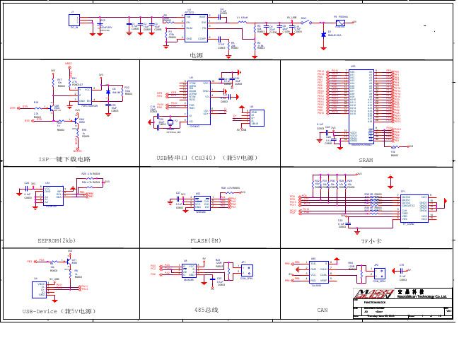
STM32开发板 SCH
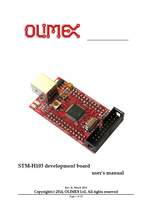
STM32-H103开发板用户指南说明书
25
11
PA4/SPI1.NSS
10
PA3/UART2.RX
12
PC4/USB-P
13
PC5
14
PB10/UART3.TX
15
P11/UART3.RX
16
PB13/SPI2.SCK
17
PB12/SPI2.NSS/I2C.SMBA 18
PB14/SPI2.MISO
19
PB15/SPI2.MOSI
20
PC6
PC7 21
22
PC8
23
+5V USB
24
PC9
25
GND
26
VIN
Page 10 of 18
JUMPER DESCRIPTION:
R-T
connects JTAG TRST signal to STM32F103RBT6 RESET
Default state closed (shorted)
VBAT
CLOCK CIRCUIT:
Quartz crystal 8Mhz is connected to STM32F103RBT6. Internal PLL circuit can multiply this frequency up to 72Mhz. 32.768 KHz quartz crystal is connected to STM32F103RBT6 for it’s internal Real Time Clock.
USBP-E
connects USB power supply to STM32F103RBT6 pin.24 PC4/ADC14 and allow to detect if the board is connected to USB host. Default state closed (shorten)
MINI-STM32 开发板入门教程.
MINI-STM32 开发板入门教程(一) 开发环境建立及其应用我们常用的 STM32 开发编译环境为 Keil 公司的 MDK (Microcontroller Development Kit) 和 IAR 公司的 EWARM.在这里我们提供了比较稳定的新版本编译软件下载:MDK3.50 点击此处下载EWARM 5.40 点击此处下载限于篇幅, 在我们的教程里面将先以 MDK 下的一个例子来介绍如何使用 MDK 进行嵌入式应用开发.MDK 安装与配置:基于 MDK 下的开发中基本的过程:(1) 创建工程;(2) 配置工程;(3) 用 C/C++ 或者汇编语言编写源文件;(4) 编译目标应用程序(5) 修改源程序中的错误(6) 测试链接应用程序----------------------------------------------------------------(1) 创建一个工程:在 uVision 3 主界面中选择 "Project" -> "New uVision Project" 菜单项, 打开一个标准对话框选择好你电脑中的保存目录后, 输入一个你的工程名字后点确认.我们的工程中建了一个名字叫 "NewProject" 的工程.从设备库中选择目标芯片, 我们的 MINI-STM32 开发板使用的是 STM32F103V8T6, 因此选中 STMicrocontroller 下对应的芯片:ARM 32-bit Cortex-M3 Microcontroller, 72MHz, 64kB Flash, 20kB SRAM,PLL, Embedded Internal RC 8MHz and 32kHz, Real-Time Clock,Nested Interrupt Controller, Power Saving Modes, JTAG and SWD,3 Synch. 16-bit Timers with Input Capture, Output Compare and PWM,16-bit 6-ch Advanced Timer, 2 16-bit Watchdog Timers, SysTick Timer, 2 SPI, 2 I2C, 3 USART, USB 2.0 Full Speed Interface, CAN 2.0B Active, 2 12-bit 16-ch A/D Converter, Fast I/O Ports选择完芯片型号后会提示是否在目标工程中加入 CPU 的相关的启动代码, 如下图所示. 启动代码是用来初始化目标设备的配置, 完成运行的系统初始化工作, 因此我们选择 "是" , 这会使系统的启动代码编写工作量大大减少.----------------------------------------------------------------(2) 配置工程:选择菜单中 "Project" -> "Option for Target" 或者选择快捷菜单中的图标:因为 MINI-STM32 开发板上使用的就是 8M 的晶振且是使用的片内的 RAM 和 ROM 因此"taget" 下我们都可以使用默认的配置;在"Output"菜单下我们需要选中 "Creat Hex File" 来生成编译好的工程代码, 此工程可以通过仿真器或者串口 ISP 烧录进开发板中.注: ISP 烧录过程我们将在入门教程二中给大家介绍."Listing" "User" 菜单中我们保持默认即可."C/C++" 菜单为我们常用的菜单, 这里简单的介绍下他们的具体功能:PreProcesser Symbols 中的 Define, Undefine 菜单表示是工程的宏定义中的变量, 我们将在今后的教程中详细介绍这个功能.Optimization 为优化选项, Level0 为不优化, 这种模式最适合调试, 因为不会优化掉代码, 基本每个用到的变量都可以打断点. Level3 为优化等级最高, 最适合生产过程中下载到芯片中的代码.Include Path 为工程中的包含路径, 一般需将 .h 文件或者库文件的地址配置进去."Asm" 和 "Link" 将在今后的高级教程中介绍."Debug" 为我们调试使用的配置选项, "Use Simulator" 为使用软件仿真. 这里根据大家手里的仿真器来选择配置环境.如果你使用的是 Ulink, 那么就选择 "Ulink Cotex Debug", 如果你选择的是 JLINK, 那么就选择 " Cotex M3 Jlink", 如果你使用的是 ST 公司出的简易仿真器 ST-Link , 那么你就选择 "ST-Link Debug".注意: 右边当中的选项 "Run to main{}" 选项如果勾上就表示仿真时进入了就会进入到main 函数, 如果没有选上就会进入初始地址, 你需要自己打断点运行到你的主程序 main 处.当插上仿真器后选择上面右图中的 Setting 后会跳出一个仿真器的配置菜单. 左边会自动识别出你的仿真器的信息.如下图为 ULINK2 的信息:对于 SWJ 选项为三线制调试, 将在后面的高级教程中介绍.右下方有两个选项:"Verify Code Download" : 表示下载后校验数据"Download to flash": 表示当仿真的时候先将目标代码下载到 Flash 中.Trace 菜单为跟踪配置, 可以实时的将一些变量使用曲线的形式实时表示出来, 我们将在今后的高级教程中介绍这一项功能.注意: 市面上目前的盗版 Ulink2 不支持这项功能, 正版的支持, Jlink 也不支持这项功能."Flash Download" 菜单用来配置使用仿真器程序下载的配置选项, 大家务必选择好和你芯片配套的选项. 如果你是使用的别人模板下修改为你的工程, 这个选项请注意一下, 如果不正确将不能将你的代码下载到芯片中.配置好 "Debug" 后, 那么 "Utilities" 可以不用配置.如果你使用的是仿真器仿真, 在你已经正确得将目标板和仿真器建立了物理连接后, 请选择正确的仿真器进行配MINI-STM32 开发板入门教程 (二) ISP 在线下载程序ISP:in system programming简介:ISP: 用写入器将code烧入,不过,芯片可以在目标板上,不用取出来,在设计目标板的时候就将接口设计在上面,所以叫"在系统编程",即不用脱离系统;应用场合: 1,ISP 程序升级需要到现场解决,不过好一点的是不必拆机器了;ISP的实现一般需要很少的外部电路辅助实现,通常可利用单片机的串行口接到计算机的RS232口,通过专门设计的固件程序来编程内部存储器。
GD STM32F407开发板介绍

金龙电子工作室GD STM32F407开发板板载:USB转串口,以太网,USB OTG,SD卡座(SDIO接口),摄像头OV7670(DCMI接口),I2S音频,2.8寸液晶屏(FSMC接口),SPI FLASH,加数度传感器等硬件资源。
主芯片:STM32F407VGT6,100PIN,Cortex-M4处理器最高运行频率为168MHz1 Mbyte Flash192+4 Kbyte SRAM支持片外Flash, SRAM, PSRAM, NOR及NAND Flash8080/6800 模式的LCD接口USB 2.0 high-speed/full-speed device/host/OTG10/100 Ethernet MAC硬件IEEE 1588v22 CAN(2.0B Active)4 UART3 SPI 最高30 Mbit2 IIS8- to 14-bit摄像头接口最高48 Mbyte/s1-bit (default), 4-bit and 8-bit SD/SDIO MMC card12-bit 0.5μs A/D12-bit D/A17 timers 最高120MHz的计数频率I/O最高频率为60MHzISP及IAP编程407板载资料1.主芯片:STM32F407VGT6,100PIN2.以太网功能(PHY:DM9161AEP)3.2.8寸彩屏模块(FSMC总线方式),带加速度传感器4.摄像头OV7670(配套)5.JTAG 20PIN标准下载口6.MICRO SD卡接口(SDIO方式)B OTG主从设备接口B转串口(PL2303HX),可用USB下载程序,做串口实验9.RTC电池座10.I2S音频DA,支持WAV播放11.电源接口,开关(LED灯)12.四个用户按键,一个复位按键,四个用户LED13.所有IO在芯片四周引出,2.54MM标准间距产品包装:金龙407开发板<一块>OV7670摄像头模组 <一个>2.8寸彩屏模块 <一块>USB电源线<一条>DVD ROM光盘<一张>。
stm32开发板原理图
Y5 1 4 3
C41 0.1uF C0603 VGND IOVDD0 IOVDD1 IOVDD2 6 14 19 CVDD CVDD0 CVDD1 CVDD2 CVDD3 RX TX 5 7 24 31 26 27 4 16 20 21 22 35 38 43 45 C35 0.1uF C0603 VGND C36 0.1uF C0603 C37 0.1uF C0603 C38 0.1uF C0603 R43 100k IOVDD R0603
C76 10uF C0805
U6 6 5 DD+ D+ D5 4 3 2 1 GND ID D+ DVBUS
PD14 PD15 PD0 PD1 PE7 PE8 PE9 PE10 PE11 PE12 PE13 PE14 PE15 PD8 PD9 PD10
PD14 PD15 PD0 PD1 PE7 PE8 PE9 PE10 PE11 PE12 PE13 PE14 PE15 PD8 PD9 PD10
5
4
3
2
1
J1 1 2 3 DC_IN R2 100k R0603 C1 0.1uF C0603 C2 10uF C0805 C3 10uF C0805 R1 179k R0603 8 3 7 1
U1 RT7272 VIN EN RLIM B00T SW FB 2 1 5 + EC2 2 100uF/25V
C42 0.01uF C0603R44 22R R0603 C43 0.01uF C0603 RIGHT R45 22R R0603
AGND
C60 18pF C0603
2
R53 1M R0603 30 31
U57 XI/CLKIN XO TXN TXP RXN RXP LINKLED ACTLED NC1 NC2 NC3 NC4 DNC VBG RSVD1 RSVD2 RSVD3 RSVD4 RSVD5 PMODE2 PMODE1 PMODE0 EXRES1 T0CAP 1V20 RSVD 1 2 5 6 25 27 46 47 12 13 7 18 38 39 40 41 42 43 44 45 10 R58 12.4k R0603 4.7uF C0603 0.01uF C0603 AGND R66 10k R0603 R65 10k R0603 AGND R64 10k R0603 R63 10k R0603 R62 10k R0603 R61 10k R0603 3V3 R60 10k R0603 R59 10k R0603 TXN TXP RXN RXP LINKLED ACTLED
STM32开发板使用说明
STM32开发板使用说明1、开发板使用到的软件及安装说明在开始学习开发板之前需要安装的软件有:1、KEIL3.80A,2、PL-2303HX驱动,3、串口调试助手,4、下载器MCUISP。
这些软件在课件文件下面的软件文件里。
具体安装步骤如下:1.KEIL3.80A的安装,打开路径:课件\软件\KEIL3.80A\MDK3.80A安装手册,根据上面的步骤安装软件。
2.PL-2303HX驱动的安装,打开路径:课件\软件\PL-2303HX新版驱动,可根据使用电脑的操作系统来选择安装的软件,如选择安装XP驱动,可打开XP驱动,根据里面的安装说明来安装软件。
一般只要运行PL-2303 Driver Installer。
exe就可以了。
3.串口调试助手的安装,打开路径:课件\软件\串口调试助手,点击sscom33。
exe即可,也可以创建快捷方式在桌面。
4.下载器MCUISP的安装,打开路径:课件\软件\下载器MCUISP,点击mcuisp。
exe 即可,也可以创建快捷方式在桌面。
2、开发环境介绍及使用说明首先是我们之前安装的keil3.80a。
再点击Project->New uVision Project如下图所示:弹出create new project 对话框,新建一个文件夹TEST,然后把工程名字设为test。
点击保存。
弹出选择器件的对话框,因为我们的开发板使用的是STM32F103RBT6 ,所以在这里我们选择STMicroelectronics 下面的STM32F103RB( 如果使用的是其他系列的芯片,选择相应的型号就可以了)。
如下图所示:点击OK,MDK会弹出一个对话框,问你是否加载启动代码到当前工程下面,这里我们选择是。
启动代码是一段和硬件相关的汇编代码。
是必不可少的!在上面点击了是以后,MDK 就把启动代码STM32F10x。
s 加入到了我们的工程下面。
如下图所示:到这里,我们就可以开始编写自己的代码了。
STM32F429I-DISCO开发板用户手册说明书

Open429Z-D User ManualContents1. Hardware introduction (2)1.1. What’s on board (2)2. Demo (4)2.1. ADC+DMA (4)2.2. CAN1 TO CAN2-Normal (5)2.3. DAC (5)2.4. DS18B20 (6)2.5. OV2640 (6)2.6. GPIO_Key (7)2.7. I2C (7)2.8. I2S_UDA1380 (8)2.9. NandFlash_SCB0 (8)2.10. SAI (9)2.11. SD_FatFS (9)2.12. SDIO (9)2.13. SPI (10)2.14. USART (11)3. Version update records (11)1. Hardware introduction 1.1. What’s on board[ Core interface ]1. STM32F429I-DISCO socketfor easily connecting the STM32F429I-DISCO 2. MCU pins connectorall the MCU I/O ports are accessible onexpansion connectors for further expansion 3. USB connectorUSB to UART via PL2303 USB TO UART board onboard MCU4. I2C1 / I2C2interface[ Other interfaces ]16. 5V DC jack17. 5V/3.3 V power input/outputusually used as power output, alsocommon-grounding with other user board 18. JTAG/SWD interfacefor debugging/programming[ Jumper ]easily connects to I2C peripherals such as I/O expander (PCF8574), FRAM (FM24CLXX), etc. 5. I2S2 / I2S3 / I2C1 interfacefor connecting I2S peripherals, such as Audio module.6. DCMI interfacefor connecting camera module 7. SDIO interfacefor connecting Micro SD module, features much faster access speed rather than SPI 8. CAN1 interfacecommunicates with accessory boards which feature the CAN device conveniently 9. CAN2 interfacecommunicates with accessory boards which feature the CAN device conveniently 10. UART3 interfaceeasily connects to RS232, RS485, USB TO 232, etc11. SPI1/SPI4 + AD/DA interfaceeasily connects to SPI peripherals such as DataFlash (AT45DBxx), SD card, MP3 module, etc MP3SPI1 features AD/DA alternative function, supports connecting AD/DA module as well 12. UART2 interfaceeasily connects to RS232, RS485, USB TO 232, etc13. 8-bit FSMC interfaceeasily connects to peripherals such as NandFlash, Ethernet, etc 14. SAI1 interfacefor connecting Audio peripherals, such as UDA1380 etc15. One-WIRE interfaceeasily connects to ONE-WIRE devices (TO-92 package), such as temperature sensor (DS18B20), electronic registration number (DS2401), etc.16. Joystick jumpershort the jumper to connect the joystick to default I/Os used in example code;open the jumper to connect the joystick to custom I/Os via jumper wires. 17. BOOT mode switchfor configuring BOOT0 pin 18. USB TO UART jumper[ Components ] 16. AMS1117-3.33.3V voltage regulator 17. PL2303USB to UART MCU 18. 5V DC jack 19. Power LED20. UART1 indicator LED 21. Joystickfive positions2. DemoKEIL MDK Version :4.7Programmer/Debugger: STM32F429I-DISCO onboard ST-LINK V2 Programming/Debugging interface: SWDConnect PC to the onboard USB TO UART connector via USB wireSerial port settings:2.1. ADC+DMA◆ OverviewAD acquisition demo◆ Hardware connectionConnect Analog Test Boardto SPI1(ADC+DAC )connector◆ Operation and resultRotate the onboard potentiometer, the below message will be printed on the serial debugging assistant:Select a proper COM port Baud rate115200Data bits 8Stop bits 1 Parity bits None Flow controlNone2.2. CAN1 TO CAN2-Normal◆ OverviewCAN demo◆ Hardware connection◆ Hardware connectionConnect the two CAN modules to theonboard CAN interfaces◆ Operation and resultYou may see the below result on the serial debugging assistant:2.3. DAC◆ OverviewDAC demo◆ Hardware connectionConnect the Analog Test Board to the SPI1(ADC+DAC )connectorConnect the Analog Test Board onboard 5Vinterface to the board onboard 5V interface viajumper wire.◆ Operation and resultYou may hear sound from the Analog Test Board2.4. DS18B20◆ OverviewDS18B20 demo◆ Hardware connectionConnect the DS18B20 module to the one-wire connector ◆ Operation and resultThe below information will be printed on the serial debugging assistant2.5. OV2640◆ OverviewCamera OV2640 demo ◆ Hardware connectionConnect the OV2640 Camera Board tothe onboard DCMMI connectorLaunch the serial debugging assistant, configuring the data as below: COM: COM3Baud rate: 115200 Data bits: 8 Parity bits: NO Stop bits: 1◆ Operation and result:Press “user” key, the captured image displayed on the serial debugging assistant:2.6. GPIO_Key◆ Overviewjoystick demo◆ Hardware connectionShort the JOYSTICK JMP on board ◆ Operation and resultPress the joystick, message will be printed on the serial debugging assistant accordingly.2.7. I2C◆ OverviewI2C EEPROM demo ◆ Hardware connectionConnect the AT24/FM24 Board to the board viaI2C connector (I2C1 or I2C2, depending on the software configuration).◆ Software configurationThe module connect to I2C1 connectorThe module connect to I2C2 connector #define Open_I2C1 //#define Open_I2C2//#define Open_I2C1 #define Open_I2C2◆ Operation and resultThe below information will be printed on the serial debugging assistant:2.8. I2S_UDA1380◆ OverviewI2S_UDA1380 demo ◆ Hardware connectionConnect the UDA1380 Board to the board via I2Sconnector.Connect the earphone to the UDA1380 Board viaLINEOUT connector◆ Operation and resultYou should hear music when press the RESET key2.9. NandFlash_SCB0◆ OverviewNandFlash demo ◆ Hardware connectionConnect the NandFlash Board to theboard via I2C2 connector.◆ Operation and resultThe below information will be printed on the serial debugging assistant:2.10. SAI◆ OverviewSAI demo◆ Hardware connectionConnect UDA1380 Board to the board via SAI1connector.Connect the earphone to the UDA1380 Board viaLINEOUT connector.◆ Operation and resultYou should hear music when press the RESET key.2.11. SD_FatFS◆ OverviewSD_FatFS demo ◆ Hardware connectionConnect the Micro SD Storage Board to theboard via SDIO connector.Insert the SD card to the Micro SD Storage Board socket.◆ Operation and resultMessage will be printed on the serial debugging assistant.2.12. SDIO◆ OverviewSDIO demo◆Hardware connectionConnect the Micro SD Storage Board to theboard via SDIO connector.Insert the SD card to the Micro SD Storage Board socket.◆ Operation and resultMessage will be printed on the serial debugging assistant.2.13. SPI◆ OverviewSPI demo◆ Hardware connectionConnect the AT45DBXX DataFlash Board via SPIconnector. (SPI1 or SPI4, depending on the software configuration◆ Software connectionModule connect to SPI1 connectorModule connect toSPI4 connector #define Open_SPI1 //#define Open_SPI4//#define Open_SPI1 #define Open_SPI4◆ Operation and resultInfo/messages printed on the serial debugging assistant:11 2.14. USART◆ OverviewUSART demo◆ Hardware connection◆ Operation and resultInfo/messages printed on the serial debugging assistant:3. Version update records VersionModification Date Author V1.0Initial Release 2014/05/17 Waveshare team。
STM32开发板操作手册说明书
Heavy Duty Surface Mount TC 26881
Strapon® RTD Sensors 22391, 22392 & 22393
–200°C to +760°C (–320°F to +1400°F) Leads to 480°C (900°F)
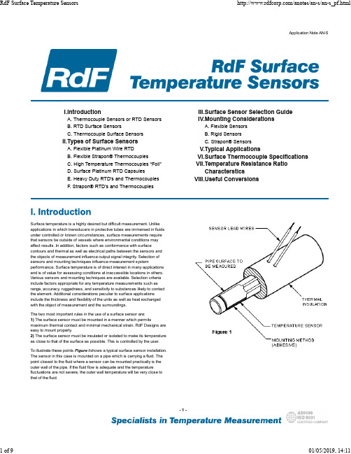
To illustrate these points Figure I shows a typical surface sensor installation. The sensor in this case is mounted on a pipe which is carrying a fluid. The point closest to the fluid where a sensor can be mounted practically is the outer wall of the pipe. If the fluid flow is adequate and the temperature fluctuations are not severe, the outer wall temperature will be very close to that of the fluid.
–200°C to +232°C (–320°F to +450°F) –200°C to260°C (–320°F to +500°F)
Thermocouple Types K, E, T or J* Grounded or Ungrounded
Resistance 100 Ω or 1000 Ω Platinum @0°C
百为STM32开发板用户手册
兼容STM3210E-EV AL开发板采用STM32F103ZET6微控制器,带USB2.0,CAN2.0A/B,I2S,I2C,USART,SPI,DAC,FSMC,SDIO,64KB SRAM,512KB Flash,JTAG和SWD仿真下载接口。
软件代码和硬件电路兼容官方STM3210E-EV AL开发板,支持UCOS,uCLinux操作系统。
一、百为STM32开发板概述:1、硬件特性:l 两种供电方式,外部5V供电和USB供电方式l 三种启动模式,下载模式、用户程序模式、内部SRAM启动模式l AK4642 I2S音频DAC,立体声耳机l MicroSD卡接口l 8Mbit SPI FLASH,1MB SRAM,128Mbit NOR Flash,64MB NAND Flashl I2C接口温度传感器芯片LM75Al 两个串口,其中一个带RTS/CTS控制l USB2.0 device接口l CAN2.0A/B兼容接口l JTAG仿真调试下载接口l 240x320 TFT彩屏l 五向游戏杆控制l 复位按键l 4个LED指示灯l RTC电池备份l 全部IO通过双排插针引出l BNC接口2、软件特性:l 简单不带库例程l 官方带库例程l 支持ST官方DEMO程序l 支持UCOS2.86+UCGUI3.90+ILI9320+TSC2046触摸l 支持FATFS+SDIO+helix软解码MP3l uCLinux操作系统l ST GUI库二、开发板硬件框图:硬件模块图:实物功能对照图:CONNETORSTM32F103ZET6SPI FLASHBOOT SELECTAK4642TF CARDAUDIO JACKADC INPUT开发板提供外部5V供电及USB供电两种方式,可通过JP13跳帽选择任意一种。
l 外部5V供电方式,JP13跳帽接PSUl USB供电方式,JP13跳帽接USB,默认USB供电方式l JP1连接1、2,VBAT接到备份电池l JP1连接2、3,VBAT接到3.3V2、启动方式l 从用户FLASH启动l 从系统存储器启动l 从内部SRAM启动开发板上有两种时钟源l X2,32KHz晶振作为RTC时钟源l X1,8MHz晶振作为MCU的时钟源,当使用内部RC震荡器作为时钟源时,可以将8MHz 晶振去掉4、复位方式STM32复位为低电平有效,开发板上有三种复位方式:l 上电复位l 通过开发板上的RESET按键复位l JTAG调试器输入复位信号5、音频AK4642音频芯片连接到STM32F103ZET6的I2S2接口,支持立体声耳机接口输出。