升降压型电源芯片XL6019规格书(中文版)
XL3005芯龙(XLSEMI)一级代理推荐降压型LED恒流驱动器芯片(常规型)
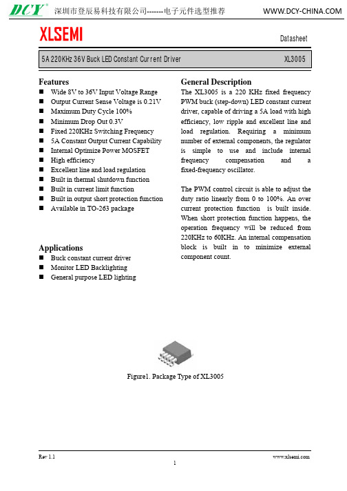
5A 220KHz 36V Buck LED Constant Current Driver XL3005FeaturesWide 8V to 36V Input Voltage Range Output Current Sense Voltage is 0.21V Maximum Duty Cycle 100% Minimum Drop Out 0.3VFixed 220KHz Switching Frequency 5A Constant Output Current Capability Internal Optimize Power MOSFET High efficiencyExcellent line and load regulation Built in thermal shutdown function Built in current limit functionBuilt in output short protection function Available in TO-263 packageApplicationsBuck constant current driver Monitor LED Backlighting General purpose LED lightingGeneral DescriptionThe XL3005 is a 220 KHz fixed frequency PWM buck (step-down) LED constant current driver, capable of driving a 5A load with high efficiency, low ripple and excellent line and load regulation. Requiring a minimum number of external components, the regulator is simple to use and include internal frequency compensation and a fixed-frequency oscillator.The PWM control circuit is able to adjust the duty ratio linearly from 0 to 100%. An over current protection function is built inside. When short protection function happens, the operation frequency will be reduced from 220KHz to 60KHz. An internal compensation block is built in to minimize external component count.Figure1. Package Type of XL30055A 220KHz 36V Buck LED Constant Current Driver XL30055A 220KHz 36V Buck LED Constant Current Driver XL3005Figure4. XL3005 Typical Application Circuit5A 220KHz 36V Buck LED Constant Current Driver XL30055A 220KHz 36V Buck LED Constant Current Driver XL30055A 220KHz 36V Buck LED Constant Current Driver XL30055A 220KHz 36V Buck LED Constant Current Driver XL30055A 220KHz 36V Buck LED Constant Current Driver XL3005 Figure13. XL3005 System Parameters Test Circuit (VIN=8V~36V, IOUT=308mA)5A 220KHz 36V Buck LED Constant Current Driver XL3005 Figure15. XL3005 System Parameters Test Circuit (VIN=8V~36V, IOUT=615mA)5A 220KHz 36V Buck LED Constant Current Driver XL3005 Figure17. XL3005 System Parameters Test Circuit (VIN=8V~36V, IOUT=925mA)5A 220KHz 36V Buck LED Constant Current Driver XL3005 Figure19. XL3005 System Parameters Test Circuit (VIN=8V~36V, IOUT=1540mA)5A 220KHz 36V Buck LED Constant Current Driver XL3005 Figure21. XL3005 System Parameters Test Circuit (VIN=8V~36V, IOUT=2140mA)5A 220KHz 36V Buck LED Constant Current Driver XL3005Figure23. XL3005 System Parameters Test Circuit (PWM DIMMING)Typical System Application (LED OVP)be limited in a suitable value by choose different zener diode when the output LED open. the zener diode Figure24. XL3005 System Parameters Test Circuit (LED OVP)5A 220KHz 36V Buck LED Constant Current Driver XL30055A 220KHz 36V Buck LED Constant Current Driver XL3005 Important NoticeXLSEMI reserve the right to make modifications, enhancements, improvements, corrections or other changes without notice at any time. XLSEMI does not assume any liability arising out of the application or use of any product described herein; neither does it convey any license under its patent rights, nor the rights of others. XLSEMI assumes no liability for applications assistance or the design of Buyers’ products. Buyers are responsible for their products and applications using XLSEMI components. To minimize the risks associated with Buyers’ products and applications, Buyers should provide adequate design and operating safeguards. XLSEMI warrants performance of its products to the specifications applicable at the time of sale, in accordance with the warranty in XLSEMI’s terms and conditions of sale of semiconductor products. Testing and other quality control techniques are used to the extent XLSEMI deems necessary to support this warranty. Except where mandated by applicable law, testing of all parameters of each component is not necessarily performed.For the latest product information, go to .。
EG1192L DC-DC电源芯片数据手册说明书
电源输入端
测试条件
-
最小
-0.3
最大
100
单位
V
EN
使能脚
-
输入电源电阻比例分
VIA
-
压后输出
FB
电压反馈输入
-
-0.3
7
V
-0.3
7
V
-0.3
7
V
VB
悬浮电源
-
VS-0.3 VS+7V
V
VS
悬浮地
-
MOS 峰值电流保护输
IS
-
入端口
TA
环境温度
-
-0.3
100
V
VS-0.3 VS+6V
V
-45
125
悬浮 驱动
VREF=0.18V
比较器 图 5-1. EG1192L 内部电路图
6 VB 1 VIN 7 VS 8 IS
2021 ©屹晶微电子有限公司 版权所有
3/8
屹晶微电子有限公司
6. 典型应用电路
EG1192L 芯片数据手册 V1.0
零功耗使能降压 DCDC 电源芯片
图 6-4. EG1192L 快充方案典型应用图
2021 ©屹晶微电子有限公司 版权所有
5/8
屹晶微电子有限公司
7. 电气特性
EG1192L 芯片数据手册 V1.0
零功耗使能降压 DCDC 电源芯片
7.1 最大额定值
无另外说明,在 TA=25℃条件下
符号
参数名称
VIN
2021 ©屹晶微电子有限公司 版权所有
1/1
屹晶微电子有限公司
EG1192L 芯片数据手册 V1.0
电源IC XC6219规格书
PRODUCT SERIES XC6219xxxxMx
Ordering Information
XC6219 123456
DESIGNATOR
DESCRIPTION
1
CE Pin Logic
23 4 5
Output Voltage Output Voltage, 100mV increments,
+2% accuracy Output Voltage, 50mV increments,
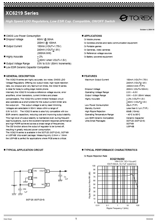
VIN=3.0V, DC+1Vp-pAC IOUT=50mA, CL=1uF (ceramics) 100
90
Ripple Rejectio源自 Rate RR (dB)80
CL
70
1µF 60
50
40
30
20
10
0
0.01
0.1
1
10
100
Ripple Frequency f (kHz)
1
R000026
: e.g. 2=3, 3=0, D 3.0V : e.g. 2=2, 3=8, 4=2 D 2.80V, +2%
: e.g. 2=2, 3=8, 4=A D 2.85V, +2%
: SOT-25 (SOT-23-5) : SOT-89-5 : USP-6B : Embossed tape, Standard feed
O
45
0.05-+00..00015
0.005+0.00 2
0.2+0.05 0.2+0.05
2
0.7 + 0.03
3
4
2
XL2596芯龙(XLSEMI)一级代理推荐降压型直流电源变换器芯片

Typical Application Circuit
Figure4. XL2596 Typical Application Circuit 12V-5V/3A
Rev 2.4 3
深圳市登辰易科技有限公司-------电子元件选型推荐
Datasheet
4 5
Rev 2.4 2
深圳市登辰易科技有限公司-------电子元件选型推荐
Datasheet
3A 150KHz 40V Buck DC to DC Converter Function Block
XL2596
Figure3. Function Block Diagram of XL2596
XL2596 General Description
The XL2596 is a 150 KHz fixed frequency PWM buck (step-down) DC/DC converter, capable of driving a 3A load with high efficiency, low ripple and excellent line and load regulation. Requiring a minimum number of external components, the regulator is simple to use and include internal frequency compensation and a fixed-frequency oscillator. The PWM control circuit is able to adjust the duty ratio linearly from 0 to 100%. An enable function, an over current protection function is built inside. When second current limit function happens, the operation frequency will be reduced from 150KHz to 50KHz. An internal compensation block is built in to minimize external component count.
升降压芯片工作原理

升降压芯片工作原理《升降压芯片工作原理》嘿,朋友们!今天咱们来聊一聊一个超酷的小玩意儿——升降压芯片。
你可能在生活中经常用到它,却没怎么注意到呢。
比如说,你的手机充电器里可能就藏着这么一个厉害的家伙。
那升降压芯片到底是干啥的呢?简单来说,它就像是一个神奇的电压魔术师。
我们都知道,不同的电器设备需要不同的电压才能正常工作。
就像不同的人对生活环境的要求不一样,有些电器喜欢高电压,有些则偏爱低电压。
想象一下,电压就像水流的压力。
如果水压太大,一些脆弱的水管(就好比一些对电压要求低的电器元件)可能就会受不了,甚至坏掉;而水压太小呢,又没办法让那些需要大水量(高电压)才能工作的大设备(比如某些功率较大的电器)正常运转。
升降压芯片的工作原理其实并不像它名字听起来那么神秘。
咱们先来说说升压的原理吧。
芯片内部就像是一个小小的能量加工厂。
它有一些特殊的电路结构,这些结构就像是一个个勤劳的小工人。
当输入的电压比较低的时候,这些小工人就开始忙活起来啦。
它们把输入的电能一点点收集起来,然后通过一种巧妙的方式把这些电能压缩到一个更小的“空间”里。
这就好比把分散的空气压缩到一个小气球里,气球里的压力(电压)就会升高啦。
这个过程中呢,涉及到一些电感、电容之类的元件。
电感就像是一个临时的电能储存器,它先把电能储存起来,然后在合适的时候和电容一起合作,把电压升高输出去。
再来说说降压的原理吧。
当输入的电压太高的时候,这个聪明的芯片又开始了它的另一种魔法。
它有点像一个流量调节阀,把高电压带来的大量电能进行合理的分配和消耗。
那些电路结构小工人呢,会让电能在一些元件里走一些“弯路”,消耗掉多余的能量,就像把湍急的河流分一部分水到旁边的小沟渠里,这样主河道(输出电压)的水压(电压)就降低了。
从数据上来说,比如说一个输入电压为5伏的电源,通过升压芯片,可能会输出12伏甚至更高的电压,这取决于芯片的设计参数。
而降压芯片呢,能把12伏的输入电压轻松地降低到3.3伏或者其他需要的电压值。
xl9021 演示板手册说明书

页数:第1 页,共4 页描述XL9021提供的演示板,用于DC5V~36V输入,输出电流2.5A的降压恒压应用演示,最高转换效率可以达到95%。
XL9021是同步整流降压型DC-DC转换芯片,固定开关频率150KHz,可减小外部元器件尺寸,方便EMC设计。
芯片具有出色的线性调整率与负载调整率,输出电压支持1.25V~25V间任意调节。
芯片内部集成短路保护、过流保护、过温保护等可靠性模块。
XL9021为标准SOP8封装,集成度高,外围器件少,应用灵活。
DEMO原理图引脚介绍物料清单页数:第2 页,共4 页DEMO实物图实物图正面实物图反面PCB布局PCB顶层截图PCB底层截图页 数:第 3 页, 共 4 页典型性能参数E f f i c i e n c y (%)Output current(A)O u t p u t v o l t a g e (V )Output current(A)5.0V 输出效率曲线 5.0V 输出线性调整率与负载调整率曲线瞬态负载响应波形瞬态负载响应波形(VIN=12V ,VOUT=5.0V ,IOUT=0.1至1A ) (VIN=24V ,VOUT=5.0V ,IOUT=0.1至1A )EN 引脚开关机波形 EN 引脚开关机波形(VIN=12V ,VOUT=5.0V ,IOUT=0.5A ) (VIN=24V ,VOUT=5.0V ,IOUT=0.5A )页数:第4 页,共4 页应用信息输入电容选择在连续模式中,转换器的输入电流是一组占空比约为VOUT/VIN的方波。
为了防止大的瞬态电压,必须采用针对最大RMS电流要求而选择低ESR(等效串联电阻)输入电容器。
对于大多数的应用,1个100uF的输入电容器就足够了,它的放置位置尽可能靠近XL9021的位置上。
最大RMS电容器电流由下式给出:IRMS≈IMAX*√VOUT(VIN-VOUT)VIN其中,最大平均输出电流IMAX等于峰值电流与1/2 峰值纹波电流之差,即IMAX=ILIM-△IL/2。
上海芯龙半导体 XL6000 系列升压芯片做升降压 SEPIC 拓朴说明书

以 XL6010 为实例来设计 SEPIC 转换器,设计要求如下所示: 输入电压(Vin):10V-24V 输出电压(Vout):12V 输出电流(Iout):1.5A 开关频率(Fsw):180KHz XL6010 是一颗升压型 DC/DC 转换器,输入电压范围 5V-32V,内置 N 沟道的 MOSFET,
IQ1( RMS )
= Iout ×
(VOUT + VIN (min) ) ×VOUT VIN (min)
= 1.5× (12 +10) ×12 10
= 7.7 A
步骤 4:选择输出二极管
二极管额定的反向电压必须高于 Vin+Vout,二极管平均电流等于满载时的输出电流。
上海芯龙半导体有限公司
XL6000 系列升压芯片做升降压 SEPIC 拓朴指导手册
SEPIC 系统设计简介
有些应用需要稳定的输出电压,该输出电压可能高于或等于也可能低于输入电压 (Vin ≤ Vout 或 Vout<Vin) ,根据这个应用,需要设计一款输入电压宽范围,输出电压恒定的 方案。
2
上海芯龙半导体有限公司
其最大开关电流 5A,开关频率 180KHz,封装类型 TO263-5L,内置 OCP、OTP 等保护电路,
工作温度-40℃--+125℃,内置软启动功能,效率可达 94%;主要应用于 PDA 供电、便携式
笔记本车载适配器等领域。
输入电压不同,输出恒压 12V 时系统应用效率图
选用肖特基二极管 D1 3A 40V SMC 封装
步骤 5:选择 SEPIC 耦合电容
Cs 的 RMS 电流为:
ICS (RMS )
屹晶微电子 EG1162 芯片数据手册说明书

2019©屹晶微电子有限公司 版权所有
1/1
屹晶微电子有限公司
EG1162 芯片数据手册 V1.0
高压大电流降压型开关电源芯片
EG1162 芯片数据手册 V1.0
1. 特性
降压同步整流方案,支持高压大电流方案。 外接一个电容可设置工作频率(0-300KHz) 2 脚 EN 外部电阻可灵活调整启动、关闭电压 UVLO 欠压锁定功能:
2019©屹晶微电子有限公司 版权所有
1/1
屹晶微电子有限公司
EG1162 芯片数据手册 V1.0
高压大电流降压型开关电源芯片
目录
1. 特性 ..................................................................................................................................................................... 1 2. 描述 ..................................................................................................................................................................... 1 3. 应用领域 ............................................................................................................................................................. 1 4. 引脚 ..................................................................................................................................................................... 2