大毅4527大功率合金电阻RLP45系列选型手册
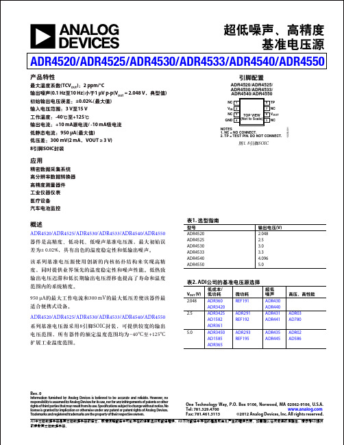
ADR4520_4525_4530_4533_4540_4550精密电压源中文技术手册
ADI中文版数据手册是英文版数据手册的译文,敬请谅解翻译中可能存在的语言组织或翻译错误,ADI不对翻译中存在的差异或由此产生的错误负责。如需确认任何词语的准确性,请参考ADI提供 的最新英文版数据手册。
ADR4520/ADR4525/ADR4530/ADR4533/ADR4540/ADR4550
目录
2.048 ADR360
大品牌采样电阻,台产大毅品牌合金电阻
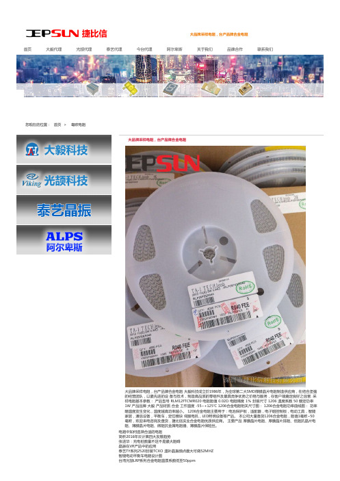
大品牌采样电阻,台产品牌合金电阻首页大毅代理光颉代理泰艺代理今台代理阿尔卑斯关于我们品牌合作联系我们大品牌采样电阻,台产品牌合金电阻大品牌采样电阻,台产品牌合金电阻 大毅科技成立於1986年,为全球第二大SMD厚膜晶片电阻制造供应商,在结合坚强的经营团队,以最先进的设 备与技术,制造高品质的零组件及最具竞争优势之价格与服务,在客户端奠定良好之信誉. 采样电阻基本参数: 产品型号 RLM12FTCMR020 电阻阻值 0.02Ω 电阻精度 1% 封装尺寸 1206 温度系数 50 额定功率1W 产品品牌 大毅 产品材质 合金 工作温度 -55~+125℃ 1206合金电阻相关尺寸图: 1206合金电阻功率曲线图: 功率随温度发生变化,温度越高功率越小。
1206合金电阻主要用于:电池保护板,适配器,电子烟控制板,电动工具,智能家居,通信设备,平衡车,定位模块 伺服电机,LED照明设备等产品。
本公司大量备货1206合金电阻,阻值1毫欧~50毫欧,欢迎来电咨询及查货,捷比信实业合金电阻优质供应商。
主要产品 厚膜晶片电阻、厚膜晶片排阻、低阻抗晶片电阻、薄膜晶片电阻、微阻抗金属电阻器、薄膜晶片保险丝。
电路中如何选择合适的电阻简析2016年云计算四大发展趋势张进华:充电桩数量不足不是最大阻碍晶振在VR产品中的应用泰艺TY系列2520封装TCXO 温补晶振频点最大可做52MHZ智能电动平衡车电路设计图台湾光颉LRP系列合金电阻温漂系数低至50ppm满足航空应用对电阻性能的新需求您现在的位置:首页 >毫欧电阻满足航空应用对电阻性能的新需求光颉0201*4贴片排阻军标级电阻 0.01%精密电阻 万分之一精度电阻 薄膜精密电阻精密电阻 合金电阻 大功率电阻 采样电阻 毫欧电阻 台湾大毅 台湾光颉 产品中心 联系方式 品牌合作 Kingbright代理 今台代理知识版权所有 Copyright © All RIGHTS RESERVED. 网站统计。
大毅合金电阻规格书-RLP系列
High Temperature Exposure
IEC60115-1- 4.23.2
JIS-C5201-4.23.2
170℃, 1000hrs
< ±1%
Low Temperature Storage
EC60115-1- 4.23.4
JIS-C5201-4.23.4
-55℃, 1000hrs
Moisture no Load
Reference
standard
IEC60115-1-4.8
JIS-C5201-4.8
IEC60115-1-4.25.1
JIS-C5201-4.25.1
Condition of Test
+25℃ ~ +125℃
Test Limits
Refer 4.0
1000hours at rated power, 70℃,
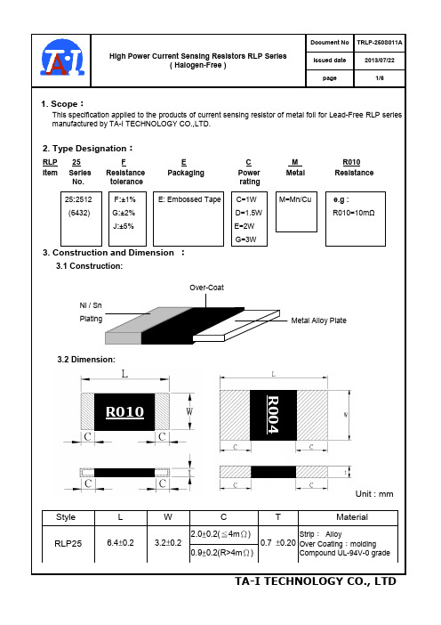
3.2 Dimension:
R004
R010
Unit : mm
Style
L
W
C
T
Material
2.0±0.2(≦4mΩ)
RLP25
6.4±0.2
3.2±0.2
Strip: Alloy
0.7 ±0.20 Over Coating:molding
0.9±0.2(R>4mΩ)
Compound UL-94V-0 grade
< ±1%
1.5hours “ON”, 0.5hour “OFF”
IEC60115-1-4.13
JIS-C5201-4.13
5 X rated power for 5s
< ±0.5%
IEC60115-1- 4.24.2.1a)
AAT 器件选型指南.pdf说明书

Part No.
Amplifiers Include
Vcc (V)
Icc
Ptot
(mA) (mW)
Toper Vio Iio (℃) (mV) (nA)
PKG
Replace Brand
LM358 LM393 LM324 LM339
2
16~32 50
500
0~70
2
2
SOP-8/DIP-8
2
2~36 0.4
128*8 256*8 512*8 1028*8 2056*8 5012*8 10024*8
Frequency Icc
Isb
(KHz)
(mA) (µA)
PKG
Replace Brand
Application
400
0.4~3 0.6~18 SOP-8/DIP-8 ATMEL/ISSI/ST/ROHM
400
400
0.4~3 0.6~18 SOP-8/DIP-8 ATMEL/ISSI/ST/ROHM
400
0.4~3 0.6~18 SOP-8/DIP-8 ATMEL/ISSI/ST/ROHM
400
0.4~3 0.6~18 SOP-8/DIP-8 ATMEL/ISSI/ST/ROHM
■ AAT General Line-up
I2-PAK
TO-220AB
TO-220IS
AAT PRODUCTS FOR CUSTOMERS
General Freque
Vcc
Device
ncy
Name
(KHz)
(V)
Vout (V)
Io (A)
7805
---
5~18
电子元器件zvp4525中文资料_数据手册_IC数据表

wcwowmh.titcphsu:n/t/.wcwowmh.titcphsu:n/t/.wcwowmh.titcphsu:n/t/.wcwowmh.titcphsu:n/t/.wcwowm.hitcthpusn:t/./cwowmwh.titcphsu:n/t/.wcwowmh.titcphsu:n/t/.wcwowmh.titcphsuZVP4525G250V P-CHANNEL ENHANCEMENT MODE MOSFETSUMMARY(m om c DESCRIPTION m o c . This 250V enhancement mode N-channel MOSFET provides users with a m om co .c t. nt competitive specification offering efficient power handling capability, high m o c . t n u impedance and is free from thermal runaway and thermally induced m o c . t n u h secondary breakdown. Applications benefiting from this device include a o c . t n u h c variety of Telecom and general high voltage circuits. t.c nt. unt hun chu ich .ic w.i SOT89 and SOT23-6 versions are also available. un hu ch ic .i w. ww ww /w FEATURES ch ic .i w. ww ww /w // :/ • High voltage i ww. www /ww //w :// s:/ ps: tps • Low on-resistance /w // :/ s: ps tp tt ht • Fast switching speed :/ s: ps tp tt ht h • Low gate drive ttps http htt ht h • Low thresholdSOT223• Complementary P-channel Type ZVN4525G• SOT223 packageAPPLICATIONS • Earth Recall and dialling switchesSDDG• Electronic hook switchesTop View• High Voltage Power MOSFET Drivers• Telecom call routers:n/t/.wcwowmh.IOD••StiDZZERSVVtcVEDUSZPPVIVEophEC44IRlPCEsui551d4IE22NM:n5-55sG2MtGGA/ta5RAITTtG/.NeACKRwcFrICNOewoHlGRawmy2Ms0h.A0tiT1(RiItcnEOcEphNhL1sue73Ss:nI)Z/tE/.wcT88wommAwmPmmEh.eeWtimmItcDbbphooTssHsussee:n(mdd/tm/.1)wcwoPQ41wm00EU00Rh.A00RNtiuuETtcnnEITphiiLttYsssu:n/t/.wcwowmh.titcphsu:n/t/.wcwowmh.titcphsu:n/t/.wcwowm.hitcthpusn:t/./cwowmwh.tiwcwowmh.titcphsu:n/t/.wcwowmh.titcphsu:n/t/.wcwowmh.titcphsu:n/t/.wcwowmh.titcphsu:n/t/.wcwowm.hitcthpusn:t/./cwowmwh.titcphsu:n/t/.wcwowmh.titcphsu:n/t/.wcwowmh.titcphsuZVP4525GABSOLUTE MAXIMUM RATINGS.PARAMETERSYMBOLLIMITUNITDrain-Source VoltageVDSS250VGate Source VoltageVGS±40VContinuous Drain Current (VGS=10V; TA=25°C)(a) ID-265mA(VGS=10V; TA=70°C)(a) ID-212mAPulsed Drain Current (c)m om c Continuous Source Current (Body Diode) m om co .c t. Pulsed Source Current (Body Diode) m om co .c t. nt un Power Dissipation at TA=25°C (a) m o c . t n u h Linear Derating Factor co .c t. nt un hu ch ic Operating and Storage Temperature RangeIDM IS ISM PD:Tj Tstg-1 -0.75-1 2 16 -55 to +150A A A W mW/°C °Cichun/t/.www.ichu:n/t/www.ichsu:n//www.icphsu://www.itcphs://www.titcps://wwwh.titps://www.https://w THERMAL RESISTANCE s: ps tp tt ht h PARAMETERttp htt ht h Junction to Ambient (a)SYMBOL RθJAVALUE 63UNIT °C/WJunction to Ambient (b)RθJA26°C/WNOTES(a) For a device surface mounted on 25mm x 25mm FR4 PCB with high coverage of single sided 1oz copper, in still air conditions(b) For a device surface mounted on FR4 PCB measured at tр5 secs.(c) Repetitive rating - pulse width limited by maximum junction temperature. Refer to Transient Thermal Impedance graph.:n/t/.wcwowmh.NFvtiooBrltctHahphgiiggesuhhs:nVvpoa/tolclt/.tiaangwcggeewobaAewmptpwph.pleilticiecatcnattiphcoioonsunnss:nd, tu/thce/.toawcrpswo.prwmoph.rtiiattcephinsud:nus/ttr/.y2wcsewoctwmorh.gtiutcidphelsuin:nes/ts/.howcuwoldwmbh.eticotcnISphsiSsudUe:nrEe/t1d/.-wwcMitwoAhRwmreCh.gHatir2dtc00tpho1su:n/t/.wcwowm.hitcthpusn:t/./cwowmwh.tiwcwowmh.titcphsu:n/t/.wcwowmh.titcphsu:n/t/.wcwowmh.titcphsu:n/t/.wcwowmh.titcphsu:n/t/.wcwowm.hitcthpusn:t/./cwowmwh.titcphsu:n/t/.wcwowmh.titcphsu:n/t/.wcwowmh.titcphsuCHARACTERISTICSZVP4525Gtitcphsu:n/t/.wcwowmh.titcphsu:n/t/.wcwowmh.titcphsu:n/t/.wcwowmh.titcphsu:n/t/.wcwowmh.titcphsu:n/t/.wcwowmh.titcphsu:n/t/.wcwowmh.titcphsu:n/t/.wcwowm.hitcthpusn:t/./cw:n/t/.wcwowmh.IStiStcUphEsu1 :n- M/tA/.RwcCwoHwm20h.0ti1tcphsu:n/t/.wcwowmh.titcphsu:n/t/.3wcwowmh.titcphsu:n/t/.wcwowmh.titcphsu:n/t/.wcwowmh.titcphsu:n/t/.wcwowm.hitcthpusn:t/./cwowmwh.tiwcwowmh.titcphsu:n/t/.wcwowmh.titcphsu:n/t/.wcwowmh.titcphsu:n/t/.wcwowmh.titcphsu:n/t/.wcwowm.hitcthpusn:t/./cwowmwh.titcphsu:n/t/.wcwowmh.titcphsu:n/t/.wcwowmh.titcphsuZVP4525GELECTRICAL CHARACTERISTICS (at Tamb = 25°C unless otherwise stated).PARAMETERSYMBOL MIN. TYP. MAX. UNIT CONDITIONS.STATICDrain-Source Breakdown VoltageV(BR)DSS -250-285VID=-1mA, VGS=0VZero Gate Voltage Drain CurrentIDSSm om c Gate-Body LeakageIGSSm om co .c t. Gate-Source Threshold VoltageVGS(th)-0.8m om co .c t. nt un Static Drain-Source On-State Resistance (1) RDS(on)com .co t.c nt. unt hun chu ich Forward Transconductance (3) nt. unt hun chu ich .ic w.i ww. w DYNAMIC (3) hu ch ic .i w. ww ww /w // Input Capacitance ic .i w. ww ww /w // :/ s: Output Capacitanceww ww /w // :/ s: ps tp Reverse Transfer Capacitance /w // :/ s: ps tp tt ht SWITCHING(2) (3) s:/ ps: tps ttp htt ht h Turn-On Delay Time ttp htt ht h Rise Timegfs80Ciss Coss Crsstd(on) tr-30-500 nA VDS=-250V, VGS=0V±1±100 nA VGS=±40V, VDS=0V-1.5 -2.0 VI =-1mA,DVDS=VGS1014ΩVGS=-10V, ID=-200mA1318ΩVGS=-3.5V, ID=-100mA200mS VDS=-10V,ID=-0.15A73 12.8 3.91pF VDS=-25 V, VGS=0V,pF f=1MHzpF1.53 3.78nsVDD =-30V, ID=-200mA ns RG=50Ω, VGS=-10V(refer to test circuit)Turn-Off Delay Timetd(off)17.5nsFall Timetf7.85nsTotal Gate Charge Gate-Source Charge Gate Drain ChargeQg2.45 3.45 nCVDS=-25V,VGS=-10V,Qgs0.22 0.31 nC ID=-200mA(refer totest circuit)Qgd0.45 0.63 nCSOURCE-DRAIN DIODEDiode Forward Voltage (1)VSD0.97 VTj=25°C, IS=-200mA,VGS=0Vm Reverse Recovery Time (3)trrm om co Reverse Recovery Charge (3)Qrr205290 ns Tj=25°C, IF=-200mA,di/dt= 100A/µs2129nCm om com .co t.c nt. (1) Measured under pulsed conditions. Width=300µs. Duty cycle ≤2% . m o c . t n u (2) Switching characteristics are independent of operating junction temperature. m o c . t n u h (3) For design aid only, not subject to production testing.:n/t/.wcwow.icphsu:n/t/.wcww.itcphsu:n/t/.www.titcphsu:n/t/wwwh.titcphsu:n//wwwh.titcphsu://wwwh.titcphs://www.hitctps://wwwh.ti ISSUE 1 - MARCH 2001 htt ht h 4wcwowmh.titcphsu:n/t/.wcwowmh.titcphsu:n/t/.wcwowmh.titcphsu:n/t/.wcwowmh.titcphsu:n/t/.wcwowm.hitcthpusn:t/./cwowmwh.titcphsu:n/t/.wcwowmh.titcphsu:n/t/.wcwowmh.titcphsuTYPICAL CHARACTERISTICSZVP4525Gtitcphsu:n/t/.wcwowmh.titcphsu:n/t/.wcwowmh.titcphsu:n/t/.wcwowmh.titcphsu:n/t/.wcwowmh.titcphsu:n/t/.wcwowmh.titcphsu:n/t/.wcwowmh.titcphsu:n/t/.wcwowm.hitcthpusn:t/./cw:n/t/.wcwowmh.IStiStcUphEsu1 :n- M/tA/.RwcCwoHwm20h.0ti1tcphsu:n/t/.wcwowmh.titcphsu:n/t/.5wcwowmh.titcphsu:n/t/.wcwowmh.titcphsu:n/t/.wcwowmh.titcphsu:n/t/.wcwowm.hitcthpusn:t/./cwowmwh.tiZVP4525GCHARACTERISTICSISSUE 1 - MARCH 2001 6TEST CIRCUITSZVP4525GISSUE 1 - MARCH 2001 7ZVP4525GPACKAGE DIMENSIONSPAD LAYOUT DETAILS4.62.0 min (3x)2.31.5 min(3x)6.82.0 min 3.8 minDimMillimetersMinMaxA6.36.7B3.33.7C–1.7D0.60.8E2.93.1F0.240.32GNOM 4.6H0.851.05K0.020.10L6.77.3MNOM 2.3InchesMinMax0.2480.2640.1300.146–0.0670.0240.0310.1140.1220.0090.013NOM 0.1810.0330.0410.00080.0040.2640.287NOM 0.0905Zetex GmbH Streitfeldstraße 19 D-81673 München Germany Telefon: (49) 89 45 49 49 0 Fax: (49) 89 45 49 49 49Zetex plc. Fields New Road, Chadderton, Oldham, OL9-8NP, United Kingdom. Telephone: (44)161 622 4422 (Sales), (44)161 622 4444 (General Enquiries) Fax: (44)161 622 4420Zetex Inc. 47 Mall Drive, Unit 4 Commack NY 11725 USA Telephone: (631) 543-7100 Fax: (631) 864-7630Zetex (Asia) Ltd. 3701-04 Metroplaza, Tower 1 Hing Fong Road, Kwai Fong, Hong Kong Telephone:(852) 26100 611 Fax: (852) 24250 494These are supported by agents and distributors in major countries world-wide © Zetex plc 2000Ths publication is issued to provide outline information only which (unless agreed by the Company in writing) may not be used, applied or reproduced for any purpose or form part of any order or contract or be regarded as a representation relating to the products or services concerned. The Company reserves the right to alter without notice the specification, design, price or conditions of supply of any product or service.ISSUE 1 - MARCH 20018。
大毅AECQ汽车级合金采样电阻RLM25选型手册

Operation life Resistance to Soldering Heat Mechanic al Shock
Resistance to vibration
Condition of Test
Test Limits
+25 ~ 125℃
Refer 4.0
T=125℃,1000hrs,Measurement at 24hrs after test conclusion.
( Halogen-Free ) AEC-Q 200-Ver D qualified
10. Reel Specification
Document No TRLM-250S149E
Issued date
2019/03/14
Page
5/6
Series RLM 25
ψA
+0
180
-3
ψB 60 ±1.0
ψC 13.0±1.0
( Halogen-Free ) AEC-Q 200-Ver D qualified
Document No TRLM-250S149E
Issued date
2019/03/14
Page
4/6
7. Number of Package: 4000 Pieces / package
8. Label:
LOT NO:
Lead-Free Current Sensing Resi stors RLM Series
( Halogen-Free ) AEC-Q 200-Ver D qualified
Document No TRLM-250S149E
Issued date
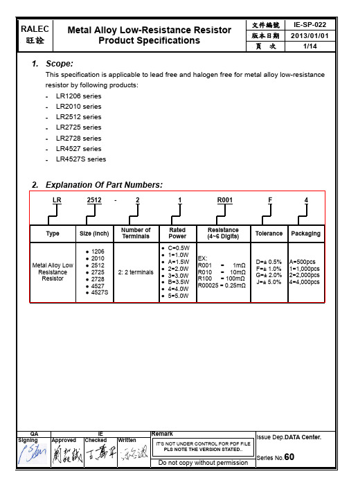
Ralec合金电阻规格书
(0.645±0.254) (0.787±0.254)
LR2512
LR2725 LR2728
0.5 ~ 3.0
1.0 & 1.5
3.1 ~ 4.0 4.1 ~75.0
75.1 ~ 100.0
0.5 ~ 3.0
2.0
3.1 ~ 4.0
0.246±0.010 (6.248±0.254)
4.1 ~75.0
文件編號 版本日期 頁次
IE-SP-022 2013/01/01
3/14
3.1 Power Derating Curve: Operating Temperature Range: - 55 ~+170 ℃ For resistors operated in ambient temperatures 70°C, power rating shell be derated in accordance with the curve below:
Do not copy without permission
Issue Dep.DATA Center.
Series No.60
RALEC
旺詮
Metal Alloy Low-Resistance Resistor Product Specifications
文件編號 版本日期 頁次
IE-SP-022 2013/01/01
5/14
Type LR4527S (without heat sink)
LR4527
Maximum
Power Resistance
Rating Range (mΩ)
L
(Watts)
Dimensions - in inches (millimeters)
大毅合金电阻

大毅合金电阻
一、简介
大毅合金电阻是一种精密度高、稳定性好的电阻产品。
它主要由合金线材、PVC外壳、阻值等组成,具有良好的电性能,特别是频率响应,具有良好的阻燃特性,耐高温、耐湿、耐高压的性能。
此外,它也具有运行稳定、耐久性能、精度高、结构紧凑、体积小、重量轻等优点。
二、性能
1、高精度:大毅合金电阻具有较高的电压精度,即最大允许误差。
2、稳定性:它具有较高的温度稳定性,即温度变化不会引起其阻值变化,而且运行可靠性高。
3、耐久性:大毅合金电阻具有良好的耐久性,有耐高温、耐湿、耐高压的性能。
4、耐腐蚀性:大毅合金电阻具有良好的耐腐蚀性,可有效耐受各种有毒气体和环境污染,能够长期稳定使用。
三、应用
大毅合金电阻有着良好的性能,所以它的应用非常广泛,主要用于电源供电、电机驱动、控制电路、信号放大器等设备上,广泛用于家用电器、专业仪器、科学仪器、自动化设备等。
- 1 -。
- 1、下载文档前请自行甄别文档内容的完整性,平台不提供额外的编辑、内容补充、找答案等附加服务。
- 2、"仅部分预览"的文档,不可在线预览部分如存在完整性等问题,可反馈申请退款(可完整预览的文档不适用该条件!)。
- 3、如文档侵犯您的权益,请联系客服反馈,我们会尽快为您处理(人工客服工作时间:9:00-18:30)。
Solderability
IEC60115-1-4.17 JIS-C5201-4.17
245±5℃, 2±0.5sec
High Temperature Exposure JIS-C5201-4.23.2 Low Temperature Storage Substrate Bending Insulation Resistance
Series RLP45
L 11.65±0.25
W 6.85±0.25
C 1.85±0.25
T 1.10 ±0.25 UNIT : mm
深圳捷比信--高品质精密元件供应商
www.jepsun.com
Document No Issued date page TRLP-450S001A 2015/11/20 2/8
2. Type Designation:
RLP45 Series No. 45→4527
F Tolerance F = ± 1% G = ± 2% J = ± 5%
E Packaging E=Embossed
J Power J = 5W
R010 Resistance
R010=10mΩ
3. Construction and Dimension :
5
Lead (Pb )-Free Assembly 3℃ / second max. 150℃ 200℃ 60 -150 seconds 217℃ 60-120 seconds 260℃ 10 seconds 6℃/second max. 8mimutes max.
Temperature (tp)2 Ramp-down Rate Time 25℃ to Peak Temperature
深圳捷比信--高品质精密元件供应商
www.jepsun.com
Document No Issued date page TRLP-450S001A 2015/11/20 1/8
Lead-Free Current Sensing Resistors RLP45 ( Halogen-Free )
1. Scope:
Lead-Free Current Sensing Resistors RLP45 ( Halogen-Free )
6. Recommended Solder Pad Dimension
B
L
A
Cu Trace
Sensing Trace
Unit: mm
Series
Resistance (mΩ)
A
B
L
RLP45
6 ≦ R ≦ 50
8.0
4.0
7.6
Note: *The copper foil minimum thickness of PCB needs 3 oz
深圳捷比信--高品质精密元件供应商
www.jepsun.com
Document No Issued date page TRLP-450S001A 2015/11/20 5/8
深圳捷比信--高品质精密元件供应商
www.jepsun.com
Document No Issued date page TRLP-450S001A 2015/11/20 8/8
Lead-Free Current Sensing Resistors RLP45 ( Halogen-Free )
15. Recommend Wave-Solder profile : (solder : Sn96.5 / Ag3 / Cu0.5)
5.0
6 ~ 50 mΩ
-55℃~+170℃
±75ppm/℃
±1% ±2% ±5%
5. Reliability Tests: Reference standard Test Limits
Refer 4.0
Test Items
Condition of Test
+25℃ ~ +125℃
Temperature Coefficient IEC60115-1-4.8 JIS-C5201-4.8 of Resistance Load Life Short Time Overload Moisture no Load Temperature cycle Resistance to Soldering Heat
This specification applied to the products of Lead-Free current sensing resistor of metal strip for Lead-Free RLP45 manufactured by TA-I TECHNOLOGY CO.,LTD.
Lead-Free Current Sensing Resistors RLP45 ( Halogen-Free )
10. Reel Specification
Series RLP45
ψA 178 ±2.0
ψB 60 ±1.0
ψC 13.0±1.0
W 25.0±1.0
T 27.4±1.0
11. Peeling Strength of Top Cover Tape
100
70 C
o
Rated Power in %
80 60 40 20 0
-50
-25
0
25
50
75
100
Ambient Temperature in C
o
125
150 170
5.2 Rated Current & Voltage
The rated Current and Voltage are calculated by the following formula:
深圳捷比信--高品质精密元件供应商
www.jepsun.com
Document No Issued date page TRLP-450S001A 2015/11/20 3/8
Lead-Free Current Sensing Resistors RLP45 ( Halogen-Free )
5.1Derating Curve
IEC60115-1-4.25.1 JIS-C5201-4.25.1 IEC60115-1-4.13 JIS-C5201-4.13 IEC60115-1- 4.24.2.1a) JIS-C5201- 4.24.2.1a) IEC60115-1-4.19 JIS-C5201-4.19 IEC60115-1-4.18 JIS-C5201-4.18
16. ECN
Engineering Change Notice: The customer will be informed with ECN if there is significant modification on the characteristics and materials described in Approval Sheet.
Lead-Free Current Sensing Resistors RLP45 ( Halogen-Free )
14. Recommend IR – Reflow profile : (solder : Sn96.5 / Ag3 / Cu0.5)
Alloyed Re-flow times : 3 times Remark : To avoid discoloration phenomena of chip on terminal electrodes, please use N2 Re-flow furnace . Iron Solder:350±10℃ , 3+1/-0 sec, 1 time Profile Feature Average ramp-up rate (Tsmax to Tp) Preheat - Temperature Min (Tsmin) - Temperature Max (Tsmax) - Time (Tsmin to Tsmax ) (ts) Time maintained above : - Temperature (TL) - Time (TL) Peak Temperature (Tp) Time within 0 ℃ of actual Peak
Test Condition: 0.1 to 0.7 N at a peel-off speed of 300 mm / min.
top cover tape 10 ~15∘ carrier tape
pull 300 mm/min standard: 0.1 ~ 0.7 N
12. Storage Conditions:
Temperature: 5℃~35℃,Humidity:40%~75%
13. Shelf Life:
2 years from manufacturing date.
深圳捷比信--高品质精密元件供应商
www.jepsun.com
Document No Issued date page TRLP-450S001A 2015/11/20 7/8
I= ������ ÷ ������
I: Rated Current(I) P: Rated Power(W)
V= ������ × ������
V: Rated Voltage(V) R: Resistance Value(Ω)
深圳捷比信--高品质精密元件供应商
www.jepsun.com
Document No Issued date page TRLP-450S001A 2015/11/20 4/8
1000hours at rated power, 70℃, < ±1% 1.5hours “ON”, 0.5hour “OFF” 5 X rated power for 5s 85℃, 85%RH, 1000hrs -55℃ & +155℃, 300cycle, 15min per extreme condition 260±5℃ for 10±1 sec < ±1% < ±1% < ±1% < ±0.5% At least 95% of surface area of electrode shall be covered with new solder < ±1% <±1% < ±0.5% >100 MΩ