单片机接口的3.5寸TFT液晶屏规格书
3.5寸TFT-LCD测试监视器说明书
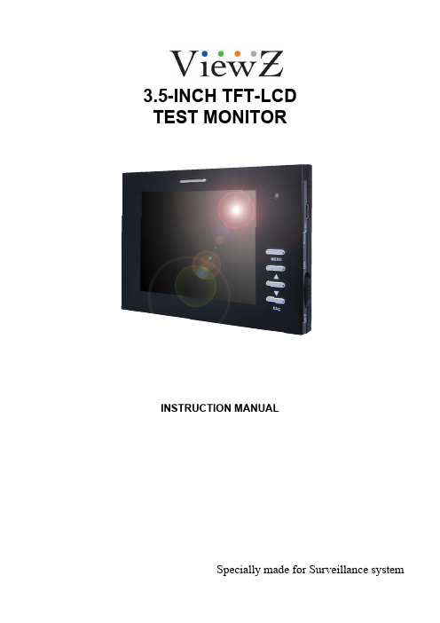
3.5-INCH TFT-LCDTEST MONITORINSTRUCTION MANUALSpecially made for Surveillance systemPlease read the following items before use.●Dear customers, thanks for using this product, we sincerely hope our products can bring you convenience, and before start to use it, please pay attention to the following items.And please keep it after reading the safety notice.1)Forbidden to use in the high temperature environment especially not allowed in hi-temperature bathroom, the most suitable working temperature for this product is approximate 0-60℃If something breaks down, please turn off the monitor, and take out the batteries, or pull out the plug of the charger. When product leaks smoke 、exception smell or other exception matter . If continue using, it may cause fire disaster or suffer shockDon’t redo or knock down the machine (Do not open the case ), if the machine breaks down or the case gets broken. Please don’t continue using ,otherwise it may cause the fire disaster or suffer shock.2)Don’t redo、heat up、over-tweak or drag the connection wire, and please don’t put heavy object on the connection wire, otherwise it may damage the wire, and cause fire disaster or suffer shock. when wire damaged, please contact the local wholesaler to change.3)Please don’t place the product in disbalance place, otherwise it may make the machine drop to get damage.4)Please use the dominated batteries, and when fixing the batteries, please do in accordance with demonstration.Please don’t heat up 、redo or knock down the battery, please don’t drop the battery or make it get hit, please don’t place the battery in the metal container. Use the dominated charger to charge the battery. any fails from the above case may cause battery explosion or leak, thereby cause the fire disaster or body harmness.5)Please use the dominated battery or AC charger. Please don’t use it at the voltage beyond the fixed range.6)If battery leaks, and the liquid comes into your eyes、skin or clothes, please wash the position touched, if necessary, please contact the doctor or dial the emergent number.7)When plug get damaged or it’s loosen when inserted into the socket, please don’t use the AC charger, otherwise it may cause fire disaster or suffer shock.8)Clean the monitor. and when not used for a long time, please take out the batteries, or pull out the plug, otherwise it may cause fire disaster or suffer shock.9)When charging finished, please pull out the plug from the socket, otherwise fire disaster may happen.10)Keep the product away from water or other liquid, otherwise there may be danger of fire disaster or shock.In order to keep your safety, please use the adapter we supplied (Regarding the damages caused by using adapters from other supplier, we are not responsible to it).11)Don’t set the machine in the place of bared sunshine.12)In order to keep it away from damage by dropping or bumping at sharp object, Please place the machine in the place where the children can not reach,When the battery’s working time is apparently shorter than new one, please change the battery.13)The machine will get heat after long time working, it belongs to normal phenomenon.14)Please don’t place the charger in the place of much dust or intensity vibration、extreme humidity or high temperature (for example: under the bare sunshine or beside the heater )15)The available voltage for the charger is AC 110~240 V / 50/60 Hz. Plug standard is various from different environment; when purchase this product, please consult relevant department to confirm the suitable plug standard. 16)During charging, the batteries and charger will get heat, it belongs to normal phenomenon, but not malfunction. If possible, please charge the battery in aeration area.Battery and power supplyThe following items state the right way to use batteries and the way to extend its lifespan Using the batteries in incorrect way will shorten its lifespan or cause to leak、overheat、fire or explode.●Battery comes out from factory with no power. Please charge it before use. and put it into the battery box whe n don’tuse it.Battery usage notice-If leaving the battery to be idle, it will lose electricity gradually. Please charge it at 1-2 day early before use·When battery in idle status, turn off the monitor, it’s a way to extend the lifespan.·The performance will reduce when battery in low temperature environment; battery can’t work normally in cold condition. place a fully charged battery in warm place. Don’t place battery close to heater or hand-warming articles.Charging Notice·Please put the batteries into the machine,and then connect the charger well.this product adopts IC to conduct electrical source management.when fit on the battery,it will conduct auto-inspection(the red light flash 2 times),if battery goes worng,the red light flash quickly;if working normally,the LED indicator light keep red.if fully charged,the red light will go out.10 minutes more charging again it’s a way to check if the charged battery is full or not.The charge time will extend if the surrounding temperature lower than 10℃ or higher than 35℃,please don’t charge the battery in the place where temperature is higher than 40℃;it stops charging when temperature under 0 ℃.it’s not allowed to charge the fully charged battery again,and you don’t have to wait to charge until the el ectricity totally runs out.·It’a normal phenomenon that battery gets heat when charge over or after use.Battery’s lifespanIn normal temperature,users can charge battery for 300 times.when the working time of consuming its full capacity apparently decrease,users need to change the battery.Storage·If long time no use after fully charged, the battery’s perfermance will weaken.·If don’t use this machine for a long time,please take the batteries ou t,and store them in a dry place,moreover the store temperature should between 15℃ and 25℃.Please don’t place it in extremely high or low temperature area.Attention:battery usage notice-Don’t transport or store the battery together with necklace、barrette and other metal object.·Don’t throw the battery into fire to heat up.·Don’t knock down or redo the battery.·Please use the dominated charger to charge.·Deal with the batteries discarded.·Don’t drop the battery or make it suffer intense vibration.·Please keep it away from water.·Please keep its connection terminal clean.·It’s the normal phenomenon that the battery and machine get heat after long time working.Alternating Current Adapter·Please just use the adapter dominated for this machine,if use other kind of adapter may cause matters to the machine. ·AC adapter for indoor use.·Make sure that DC plug connect to the monitor firmly.·Please turn off the monitor before pull out the plug.·Don’t use it in other devices.·Don’t knock it down yourself.·Don’t place it in high temperature or humidy area.·Please don’t let it suffer intense shake·It’s a normal phenomenon that the adapter buzzs or get heat when using.·If adapter cause wireless interference,please reset the antenna.Product UseIn order to make sure of the normal working,please don’t let the machine get hit or shake.Electric interferenceThis product may cause interference to the medical and aviatic devices.before you use it in the hospital or airport,please consult the hospital the airline company.Liquid crystalIf screen suffered damage,please avoid to touch the liquid crystal.if any case of the following happens,please do as we show.·If liquid crystal gets to your skin,please clean the position with cloth,then daub some soap and then wash it.·If liquid crystal comes into your eyes, please flush the eye with water more than 15minutes,and then ask for help from doctor.·If drink the liquid crystal by mistake,please gargle with water,and drink much water to help throw up,and then consult the doctor.Debug The MachineBefore start to monitor the important spot,please adjust the machine to make sure of its normal working.we are not responsible to any damage or benefit loss caused by product’s malfunction.ClaimSpecification subject to change without notice, we have the final explaination right to do a explaination to this manual. ·The screen is made from high precise technology,still there would be brightness dot or color abnormity on screen sometimes.it’s the normal phenomenon to this kind of LCD,but not failure.·When fall acrosse wireless interference( such as magnetic field、static or circuit noise),the abnormity display may happen.AccessoryPower Charger 1pcWall mount bracket 1pc1.2V AA nickel-hydrogen battery 4pcsA V cable #1( video input) : 1pcAv cable #2 (video output): 1pcWrist strap 1 pcUsers’manual 1pcWarranty card 1pcAppearance and function illustrationMenu adjustmentBrightness Brightness adjustment: Users can change the brightness and darkness of image by adjusting the parameter according to his personal requirement. Firstly, press MENU key to enter main menu interface, and then press “▲”key or “▼”key to confirm this submenu, then press “▲”or “▼”to adjust the brightness and darkness of image. Press ESC key to exist main menu.Contrast Contrast adjustment: Users can change the contrast of image by adjusting the parameter according to his personal requirement. Firstly, press MENU key to enter main menu interface, press MENU key to select downwards(moving the yellow cursor to this submenu),and then press “▲”key or “▼”key to confirm this submenu, in the end press “▲”or “▼”to adjust the contrast of image. Press ESC key to exist main menu.Saturation Saturation adjustment: Users can change the saturation of image by adjusting the parameter according to his personal requirement. Firstly, press MENU key to enter main menu interface, press MENU key to selectdo wnwards(moving the yellow cursor to this submenu),and then press “▲”key or “▼”key to confirm this submenu, in the end, press “▲”or “▼”to adjust the saturation of image. Press ESC key to exist main menu.Sharpness Sharpness: Users can change the sharpness of image by adjusting the parameter according to his personal requirement. Firstly, press MENU key to enter main menu interface, press MENU key to select downwards(moving the yellow cursor to this submenu),and then press “▲”key or “▼”key to confirm this submenu, in the end, press “▲”or “▼”to adjust the sharpness of image. Press ESC key to exist main menu.V olume V olume adjustment: Users can change the volume of image by adjusting the parameter according to his personal requirement. Firstly, press MENU key to enter main menu interface, press MENU key to select downwards(moving the yellow cursor to this submenu),and then press “▲”key or “▼”key to confirm this submenu, then press “▲”or “▼”to adjust the volume of image. Press ESC key to exist main menu.Language English / Italian / ChineseInstallation Illustration Battery fixing1.Product fixing methodUsers have four methods to fix this product, you can choose the accessories supplied to fix according to the various situation.⑴Portable: APut it on your arms by using the wrist strap.(this method is usually suitable to outdoor working or or indoor camera lens adjustment in construction field)⑵ Portable: BHanging the machine at your waist.(3) Fixing on wall :Fix the machine on wall by using the wall bracket.(4)Normal MethodOpen the multi-function bracket to stand the machine on the table-board.2.OPERATION1、Put the batteries into machine according to the direction marked with “+” “-”.2、Insert the A V cable 1 (including power output cable) to the jack in position 9of the illustration. And then connect the red RCA connecter to video signal port, and the white one to audio port.3、Switch the power switch to “ON” side.4、If you need to output A V signal , insert A V cable 2 to the jack in position 10 of the illustration. Yellow cable for video output, white one for audio output.5、If powerless, you can charge it as it’s working. Conn ect the charger to position 7 of the illustration.6、When the image comes to be normal, you can adjust it by key 3、4、5 and 6.showed in the illustration.SpecificationTrouble shootingBefore calling for repair, please refer to this section to see whether you can solve it by yourself; if you need help, please contact our after sale service centre or our wholesaler.。
3.5寸液晶屏规格书SGC035COM—54PIN
Product SpecificationsCustomerDescription 3.45” TFT LCD ModuleModel Name SGC035COM—54PINDate 2008/6/13Doc. No.Revision BCustomer ApprovalDateThe above signature represents that the product specifications, testing regulation, and warranty in the specifications are acceptedEngineeringCheck Date Prepared DateDoris2008/6/13CONTENTSNo. ITEM PAGE0 RECORD OF REVISION 31 SUMMARY 42 FEATURES 43 GENERAL SPECIFICATIONS 44 ABSOLUTE MAXIMUM RATINGS 45 ELECTRICAL CHARACTERISTICS 56 DC CHARATERISTICS 67 AC CHARACTERISTICS 6~108 OPTICAL CHARATERISTIC 119 TOUCH PANEL 14~1510 INTERFACE 16~1911 BLOCK DIAGRAM 2012 QUALITY ASSURANCE 2113 OUTLINE DRAWING 2214 PACKAGE INFORMATION 2315 PRECAUTIONS 24~26RECORD OF REVISIONSRevision Date Page DescriptionA 2008/2/12 all New CreationB 2008/6/13 18 LCM PIN Definition1. SUMMARYThis technical specification applies to 3.45“color TFT-LCD panel. The 3.45“ color TFT-LCD panel is designed for GPS, camcorder, digital camera application and other electronic products which require high quality flat panel displays. This module follows RoHS.2. FEATURESHigh Resolution: 230,400 Dots (320 RGB x 240). SGC 035COM—54PIN is atransmissive type color active matrix liquid crystal display (LCD) which uses amorphous thin film transistor (TFT) asswitching devices. This product is composed of a TFT LCD panel, driver ICs, FPC, backlight unit and touch panel.,3. GENERAL SPECIFICATIONSParameter Specifications Unit Screen size 3.45(Diagonal) InchDisplay Format 320 RGB x 240 DotActive area 70.08(H) x 52.56(V) mmDot size 73x 219 umPixel Configuration RGB-Stripe Outline dimension 76.9(W) x 63.9(H) x 3.3(D) mm Display Mode Normally white/Transmissive Surface Treatment Haze 20% Display Garmut NTSC 60% Input Interface Digital 24-bit RGB/SERIALRGB/CCIR656/CCIR601Weight (31) g View Angle direction 6 o’clockOperation -20~70 ℃Temperature RangeStorage -30~80 ℃4. ABSOLUTE MAXIMUM RATINGSItem Symbol Condition Min. Max. Unit Remark Power Voltage DVDD,AVDD GND=0 -0.3 5.0 V Input SignalVoltage V in GND=0 -0.3 VDD+0.3 VNOTE Logic OutputVoltageV OUT GND=0 -0.3 VDD+0.3 V NOTENote: Device is subject to be damaged permanently if stresses beyond those absolute maximum ratings listed above1. Temp. ≤ 60℃, 90% RH MAX.Temp. > 60℃, Absolute humidity shall be less than 90% RH at 60℃2.5. ELECTRICAL CHARACTERISTICS 5.1. Operating conditions:Parameter SymbolRatingMin. Typ. Max.Unit ConditionPower Voltage VCC 3.0 3.3 3.6 V Digital Operation CurrentIcc 8.6 mA Gate On Power VGH 14 15 18 V Gate Off Power VGL -11-10 -8V Vcom High Voltage VcomH 3.7 V Note1 Vcom low VoltageVcomL-1.6VNote1Vcom level max VcomA 6 VNote1. VcomH& VcomL :Adjust the color with gamma data. Vp-p should be higher then4V.(Option 5V)Note: Please power on following the sequence VCC Æ VDD5.2 LED driving conditionsParameter Symbol Min. Typ. Max. Unit Remark LED current- 20 - m A Power Consumption - 400 420 mW LED voltage VBL+ 18.619.8 21 V Note 1 LED Life Time - (50,000)- - HrNote 2,3Note 1 : There are 1 Groups LEDILEDNote 2 : Ta = 25℃Note 3 : Brightess to be decreased to 50% of the initial value深圳宏辉成液晶显示有限公司/6. DC CHARATERISTICSParameter SymbolRatingUnit Condition Min. Typ. Max.Low level input voltage V IL 0-0.3VCCVHight level input voltage V IH0.7VCC-VCC V7. AC CHARATERISTICSDigital Parallal RGB interfaceSignal Item Symbol Min Typ Max UnitFrequency Tosc - 156 - ns Dclk High Time Tch - 78 - nsLow Time Tcl - 78 - nsDataSetup Time Tsu 12 - - nsHold Time Thd 12 - - nsPeriod TH - 408 - Tosc Pulse Width THS 5 30 - ToscHsyncBack-Porch Thb 38 ToscDisplay Period TEP - 320 - ToscHsync-den time THE 36 68 88 TsocFront-Porch Thf - 20 - ToscPeriod Tv - 262 - THPulse Width Tvs 1 3 5 TH Vsync Back-Porch Tvb - 15 - TH Display Period Tvd - 240 - THFront-Porch Tvf 2 4 - TH1. Thp + Thb = 68, the user is make up by yourself.2. Tv = Tvs + Tvb + Tvd + Tvf , the user is make up by yourself.3.When SYNC mode is used,1st data start from 68th Dclk after Hsync fallingDigital Serial RGB interfaceSignal Item Symbol Min Typ Max Unit Frequency Tosc - 52 - ns Dclk High Time Tch - 78 - ns Low Time Tcl - 78 - nsData Setup Time Tsu 12 - - nsHold Time Thd 12 - - nsPeriod TH - 1224 - Tosc Pulse Width THS 5 90 - ToscHsyncBack-Porch Thb 114 ToscDisplay Period TEP - 960 - Tosc Hsync-den time THE 108 204 264Front-Porch Thf - 60 - ToscPeriod Tv - 262 - THPulse Width Tvs 1 3 5 THVsync Back-Porch Tvb - 15 - THDisplay Period Tvd - 240 - THFront-Porch Tvf 2 4 - TH Note: 1. Thp + Thb = 204, the user is make up by yourself.2. Tv = Tvs + Tvb + Tvd + Tvf , the user is make up by yourself.3. When SYNC mode is used,1st data start from 204th Dclk after Hsync fallinCCIR601/656 InterfaceSignalData Setup Time Tsu 12 - - ns Hold Time Thd 12 - - ns深圳宏辉成液晶显示有限公司/[_//f+--------------------H " "'= 1560--------------------+jInvalid Data Inva l i d Da t a018,0"'=DOTCLK In va li d DataIn v a l i d Data]---...t--f------------H018, =1440-------------+jslrL//RR[7:0]In va lid DataIn va l i d Dataf---- t.<sP = HBP[6:0]'4+STH[1:0'1-- *. - ----------- IH0,se = 128--- --- ----.!Figure1 CCIR601 Horizontal Timing深圳宏辉成液晶显示有限公司 /手机 : 133 166 766 58 MSN: lcd.sales@ QQ:1378107648Doc. No.SEL[2:0] = 100- 111, NTSCVSYNC HSYNCRR[7:0]tveP = VBP[6:0]DL1DL2DL3IDL2391DL240I---ODD Field VSYNCEVEN FieldHSYNCRR[7:0]tvsP= VBP[6:0] + 1·IODD FieldI IDL1DL2DL3IDL2391DL240ISEL[2:0] = 100- 111, PAL, PALM=OEVEN VSYNCHSYNCRR[7:0]tvsP= VBP[6:0]DL1DL2DL3IDL2791DL280IODD Field VSYNCEVEN Fi l eHSYNCRR[7:0]tvsP= VBP[6:0] + 1·IODD FieldI IDL1DL2DL3IDL2791DL280ISEL[2:0] = 100 - 111, PAL, PALM=1EVEN VSYNCHSYNCRR[7:0]tveP= VBP[6:0]DL1DL2DL3IDL2871DL288 1ODD Field VSYNCEVEN Fi l eHSYNCI深圳宏辉成液晶显示有限公司 /手机 : 133 166 766 58 MSN: lcd.sales@ QQ:1378107648IRR[7:0]lvsP= VBP[6 0] + 1·IDL1DL2DL3IDL287 1DL288 1Figure1CCIR601 Vertical Timing深圳宏辉成液晶显示有限公司 /手机 : 133 166 766 58 MSN: lcd.sales@ QQ:1378107648Figure2 CCIR656 Horizontal Timing深圳宏辉成液晶显示有限公司 /手机 : 133 166 766 58 MSN: lcd.sales@ QQ:1378107648Figure2 CCIR656 Vertical Timing深圳宏辉成液晶显示有限公司 /手机 : 133 166 766 58 MSN: lcd.sales@ QQ:1378107648Figure 3Digital RGB NTSC mode Vertical Data Format for 262THH cycle = 1224tHBP = 204HDISP = 960t HFP = 60DOTCLKHSYNCPixel DataDumm yD0D1----------D 957 D 958 D 959Dum mya ) Horizontal Data Transaction Tim ing V cycle = 262 Lines t VBP = 18VSYNC VDISP = 240 Lines t VFP = 4HSYNC Line 0 b ) Vertical Data Transaction Tim ing Line 239深圳宏辉成液晶显示有限公司 /手机 : 133 166 766 58 MSN: lcd.sales@ QQ:1378107648Figure 3 Data Transaction Timing in Serial RGB (8 bit) Interface (SYNC Mode)深圳宏辉成液晶显示有限公司 /手机 : 133 166 766 58 MSN: lcd.sales@ QQ:1378107648Figure3 Data Transaction Timing in Serial RGB (8 bit) Interface (DE Mode)深圳宏辉成液晶显示有限公司 /手机 : 133 166 766 58 MSN: lcd.sales@ QQ:1378107648Figure3Data Transaction Timing in Parallel RGB (24 bit) Interface (SYNC Mode)深圳宏辉成液晶显示有限公司 /手机 : 133 166 766 58 MSN: lcd.sales@ QQ:1378107648Figure4 Data Transaction Timing in Parallel RGB (24 bit) Interface (DE Mode)7.1.1 Standby ON/OFF Control LQ35NC211 has a power ON/OFF sequence control function. When STB pin is pulled L,blank data is outputted for 5-frames first, form the falling edge of the following VSYNC signal. The blank data would be gray level 255 for normally white LC.Figure5 Standby ON/OFF Control 7.1.2 Clock and Sync waveforms深圳宏辉成液晶显示有限公司 /手机 : 133 166 766 58 MSN: lcd.sales@ QQ:1378107648Figure6 CLK and IHS timing waveformTV FTC LTH B7.2 Reset Timing ChartThe RESET input must be held at least 1ms after power is stable8. OPTICAL CHARATERISTICTa=25±2℃, ILED=20mA Item Symbol Condition Min. Typ. Max. Unit Remark Response timeTr θ=0°、Φ=0°Tf- 10 ms- 15 msNote 3,5 Contrast ratio CRAt optimizedviewing angle300 400 - - Note 4,5 Color ChromaticityWhiteRedGreenBlueWxθ=0°、Φ=0WyRxθ=0°、Φ=0RyGxθ=0°、Φ=0GyBxθ=0°、Φ=0By(0.26) (0.31) (0.36) Note 2,6,7(0.28) (0.33) (0.38)Hor.ΘR(50) (60)Viewing angleΘL CR≧10(50) (60)Deg. Note 1Ver.ΦT(40) (50)ΦB(45) (55)Brightness - - 180 200 - cd/m2Center ofdisplayTa=25±2℃, I L=20mANote 1: Definition of viewing angle rangeFig. 8-1 Definition of viewing angleNote 2: Test equipment setup:After stabilizing and leaving the panel alone at a driven temperature for 10 minutes, the measurement should be executed. Measurement should be executed in a stable, windless, and dark room. Optical specifications are measured by Topcon BM-7 luminance meter 1.0° field of view at a distance of 50cm and normal direction.Fig. 8-2 Optical measurement system setupNote 3: Definition of Response time:The response time is defined as the LCD optical switching time interval between “White” state and“Black” state. Rise time, Tr, is the time between photo detector output intensity changed from 90﹪to 10﹪. And fall time, Tf, is the time between photo detector output intensity changedfrom10﹪to 90﹪.Note 4: Definition of contrast ratio:The contrast ratio is defined as the following expression.Contrast ratio (CR)= Luminance measured when LCD on the “White” stateLuminance measured when LCD on the “Black” stateNote 5: White Vi = V i50 ± 1.5VBlack Vi = Vi50 ± 2.0V“±” means that the analog input signal swings in phase with VCOM signal. “±” means that the analog input signal swings out of phase with VCOM signal.The 100% transmission is defined as the transmission of LCD panel when all the input terminals of module are electrically opened.Note 6: Definition of color chromaticity (CIE 1931)Color coordinates measured at the center point of LCDNote 7: Measured at the center area of the panel when all the input terminals of LCD panel are electrically opened.Brightness (min)Note 8 : Uniformity (U) = x 100%Brightness (max)9. TOUCH PANELNA10. INTERFACE10.1. LCM PIN DefinitionPin Symbol I/O Function Remark1 LED- I Backlight LED Ground2 LED- I Backlight LED Ground3 LED+ I Backlight LED Power4 LED+ I Backlight LED Power5 Y1 I Top electrode ,6 X1 I Right electrode7 NC Not Use8 /RESET - Hardware Reset9 SPENA I SPI Interface Data Enable Signal Note 310 SPCLK I SPI Interface Data Clock Note 311 SPDAT I SPI Interface Data Note 312 B0 I Blue Data Bit 013 B1 I Blue Data Bit 114 B2 I Blue Data Bit 215 B3 I Blue Data Bit 316 B4 I Blue Data Bit 417 B5 I Blue Data Bit 518 B6 I Blue Data Bit 619 B7 I Blue Data Bit 720 G0 I Green Data Bit021 G1 I Green Data Bit122 G2 I Green Data Bit223 G3 I Green Data Bit324 G4 I Green Data Bit425 G5 I Green Data Bit526 G6 I Green Data Bit627 G7 I Green Data Bit728 R0 I Red Data Bit0 /DX0 Note 429 R1 I Red Data Bit1 /DX1 Note 430 R2 I Red Data Bit2 /DX2 Note 431 R3 I Red Data Bit3 /DX3 Note 432 R4 I Red Data Bit4 /DX4 Note 4Control the input data format /floatingControl the input data formatControl the input data formatNot UseData Enable Input54 AVSS INote:1. The mode control (SEL2) not use ,it can’t control CCIR601 interface , If not use CCIR601 ,itcan floating.2. For digital RGB input data format, both SYNC mode and DE+SYNC mode are supported. If DEsignal is fixed low, SYNC mode is used. Otherwise, DE+SYNC mode is used.Suggest used SYNC mode!!Suggest the DE signal usually pull low.3. usually pull high.4. IF select serial RGB or CCIR601/656 input mode is selected,only DX0-DX7 used,and the other short to GND, Onlyselected serial RGB、CCIR601/656 interface,DX BUS will enable,Digital input mode DX0 is LSB and DX7 is MSB.5. Control the input data formatDoc. No.10.2 SPI timing CharacteristicsFigure8 SPI read、write timingFigure9 SPI timingFigure10 SPI Reference program10.3 SPI Register DescriptionWill be showing on Application Note From Chihsin .10.4 Basic Display Color and Gray ScaleColorRedMSB LSBInput Color DataGreenMSB LSBBlueMSBLSBR7 R6 R5 R4 R3 R2 R1 R0 G7 G6 G5 G4 G3 G2 G1 G0 B7 B6 B5 B4 B3 B2 B1 B0BasicColorsBlack Red(255) Green(255) Blue(255)CyanMagenta Yellow White 0 0 0 1 1 1 0 0 0 0 0 0 0 0 0 1 1 1 1 1 1 1 1 1 0 0 0 0 0 0 0 1 1 1 1 1 0 0 0 0 0 0 0 1 1 0 0 0 0 0 0 0 0 0 0 0 0 1 1 1 1 1 1 1 0 0 1 1 1 1 1 1 1 1 1 1 1 1 1 1 0 0 0 0 0 0 1 1 1 0 0 0 1 1 1 0 0 0 1 1 1 1 1 1 0 0 0 0 0 0 1 1 1 0 0 0 1 1 1 0 0 0 1 1 1 1 1 1 0 0 0 0 0 0 0 0 0 1 1 1 1 1 1 1 1 1 0 0 0 1 1 1 0 0 0 0 0 0 0 0 0 0 0 0 0 0 0 1 1 1 1 1 1 1 1 1 1 1 1 1 1 1 0 0 0 0 0 1 1 1 1 1RedRed(0) Dark Red(1) Red(2) :Red(253) Red(254)Red(255) Bright0 0 0 0 0 0 0 0 0 : : : 1 1 1 1 1 1 1 1 10 0 0 0 0 0 0 0 0 0 0 1 0 0 0 0 0 1 0 0 0 : : : : : : : 1 1 1 0 1 0 0 1 1 1 1 0 0 0 1 1 1 1 1 0 0 0 0 0 0 0 0 0 0 0 : : : 0 0 0 0 0 0 0 0 0 0 0 0 0 0 0 0 0 0 : : : 0 0 0 0 0 0 0 0 0 0 0 0 0 0 0 0 0 0 : : : 0 0 0 0 0 0 0 0 0 0 0 0 0 00 0 0 0 0 0 0 0 0 0 : : : : : 0 0 0 0 0 0 0 0 0 0 0 0 0 0 0GreenGreen(0) Dark 0 0 0 Green(1) 0 0 0 Green(2) 0 0 0:: : : Green(253) 0 0 0 Green(254) 0 0 0 Green(255)Bright 0 0 0 0 0 0 0 0 0 0 0 0 0 0 0 0 0 0 0 0 0 0 0 0 : : : : : : : 0 0 0 0 0 1 1 0 0 0 0 0 1 1 0 0 0 0 0 1 1 0 0 0 0 0 0 0 0 0 : : : 1 1 1 1 1 1 1 1 1 0 0 0 0 0 1 0 1 0 : : : 1 0 1 1 1 0 1 1 1 0 0 0 0 0 0 0 0 0 : : : 0 0 0 0 0 0 0 0 0 0 0 0 0 0 0 0 0 0 0 0 0 0 0 0 : : : : : 0 0 0 0 0 0 0 0 0 0 0 0 0 0 0Blue Blue(0) Dark Blue(1) Blue(2): Blue(253)Blue(254)Blue(255) Bright0 0 0 0 0 0 0 0 0 : : : 0 0 0 0 0 0 0 0 00 0 0 0 0 0 0 0 0 0 0 0 0 0 0 0 0 0 0 0 0 : : : : : : : 0 0 0 0 0 0 0 0 0 0 0 0 0 0 0 0 0 0 0 00 0 0 0 0 0 0 0 0 : : : 0 0 0 0 0 0 00 0 0 0 0 0 0 0 0 : : : 0 0 0 0 0 0 00 0 0 0 0 0 0 0 0 : : : 1 1 1 1 1 1 10 0 0 0 0 0 0 0 0 1 0 0 0 1 0 : : : : : 1 1 1 0 1 1 1 1 1 0 1 1 1 1 111. BLOCK DIAGRAMCUSTOMER’S SYSTEMDigital24-bits,CCIR656, CCIR601,SERIAL SPCLK, SPDAT, Hsync, Vsync, DCLK12. QUALITY ASSURANCENo. Test Items Test Condition REMARK 1 High Temperature Storage Test Ta=80℃ Dry 240h 2 Low Temperature Storage Test Ta=-30℃ Dry 240h 3 High Temperature Operation Test Ta=70℃ Dry 240h 4 Low Temperature Operation Test Ta=-20℃ Dry 240h5High Temperature and High HumidityOperation TestTa=60℃ 90%RH 240h6 Electro Static Discharge Test7 Shock Test (non-operating)8 Vibration Test (non-operating) Panel surface / top case. Contact / Air :±6KV / ±8KV ,150pF ,330ΩShock Level : 100GWaveform : Half Sinusoidal WaveShock Time : 6msNumber of Shocks : 3 times for each ±X, ±Y, ±Z direction Frequency range: 10Hz ~ 550HzStoke :1.3mmSweep : 1.5G, 33.3~400HzVibration : Sinusoidal Wave, 1Hrsfor X,YZ direction.Non-operating9 Thermal Shock Test-20℃(0.5h) ~ 70℃(0.5h) / 100cycles***** T a = Ambient TemperatureNote:1. The test samples have recovery time for 2 hours at room temperature before the function check. In the standard conditions, there is no display function NG issue occurred.2. All the cosmetic specifications are judged before the reliability stress.Doc. No.13. OUTLINE DRAWING Rev: BPage: 27 of 30Date: 2008/6/13ITO Film:Sheet Resistance 200~900ΩITO Glass:Sheet Resistance 200~900ΩSurface hardness MIN. 3H此區顯示為 lable 的貼附範圍lable 的實際大小則依據B L specComponent H=1.5mmX2 Y1Y2 X1 +Kapton1DATEDATEDATE 2007-11-192007-11-19TITLE:8Doc. No.14.PACKAGE INFORMATION Rev: BPage: 28 of 30Date: 2008/6/132APPROVED DATEE奇信電子股份有限公司DWG. NO.: HS-P-03450915QH011CHECKED DATE REV.:UNIT: SCALE:SHEET:DESIGNER Lake Chao DATE 01/15"07SIEZ: A2PART NO.: 09150190-001:1 1/14 5DRAWER Lake Chao7DATE 01/15"078TITLE:包材圖15 RECAUTIONSPlease pay attention to the following when you use this TFT LCD module.15.1 MOUNTING PRECAUTIONS(1) You must mount a module using arranged in four corners or four sides.(2) You should consider the mounting structure so that uneven force (ex. Twisted stress) is notapplied to the module.And the case on which a module is mounted should have sufficient strength so that external force is not transmitted directly to the module.(3) Please attach a transparent protective plate to the surface in order to protect the polarizer.Transparent protective plate should have sufficient strength in order to the resist external force.(4) You should adopt radiation structure to satisfy the temperature specification.(5) Acetic acid type and chlorine type materials for the cover case are not describe becausethe former generates corrosive gas of attacking the polarizer at high temperature and the latter causes circuit break by electro-chemical reaction.(6) Do not touch, push or rub the exposed polarizers with glass, tweezers or anything harderthan HB pencil lead. And please do not rub with dust clothes with chemical treatment.Do not touch the surface of polarizer for bare hand or greasy cloth. (Some cosmetics are determined to the polarizer)(7) When the surface becomes dusty, please wipe gently with adsorbent cotton or other softmaterials like chamois soaks with petroleum benzene. Normal-hexane is recommended for cleaning the adhesives used to attach front / rear polarizers. Do not use acetone, toluene and alcohol because they cause chemical damage to the polarizer.(8) Wipe off saliva or water drops as soon as possible. Their long time contact with polarizercauses deformations and color fading.(9) Do not open the case because inside circuits do not have sufficient strength.15.2 OPERATING PRECAUTIONS(1) The spike noise causes the mis-operation of circuits. It should be lower than followingvoltage:V=±200mV(Over and under shoot voltage)(2) Response time depends on the temperature. (In lower temperature, it becomes longer.)(3) Brightness depends on the temperature. (In lower temperature, it becomes lower)And in lower temperature, response time (required time that brightness is stable after turned on) becomes longer.(4) Be careful for condensation at sudden temperature change. Condensation makes damageto polarizer or electrical contacted parts. And after fading condensation, smear or spot will occur.(5) When fixed patterns are displayed for a long time, remnant image is likely to occur.(6) Module has high frequency circuits. Sufficient suppression to the electromagneticinterference shall be done by system manufacturers. Grounding and shielding methods may be important to minimize the interference.15.3 ELECTROSTATIC DISCHARGE CONTROLSince a module is composed of electronic circuits, it is not strong to electrostatic discharge.Make certain that treatment persons are connected to ground through wristband etc. And don’t touch interface pin directly.15.4 PRECAUTIONS FOR STRONG LIGHT EXPOSUREStrong light exposure causes degradation of polarizer and color filter.15.5 STORAGE When storing modules as spares for a long time, the following precautions are necessary. (1) Store them in a dark place. Do not expose the module to sunlight or fluorescent light. Keep the temperature between 5℃ and 35℃ at normal humidity. (2) The polarizer surface should not come in contact with any other object. It is recommended that they be stored in the container in which they were shipped. 15.6 HANDLING PRECAUTIONS FOR PROTECTION FILM (1) When the protection film is peeled off, static electricity is generated between the film and polarizer. This should be peeled off slowly and carefully by people who are electrically grounded and with well ion-blown equipment or in such a condition, etc. (2) The protection film is attached to the polarizer with a small amount of glue. Is apt to remain on the polarizer.Please carefully peel off the protection film without rubbing it against the polarizer. (3) When the module with protection film attached is stored for a long time, sometimes there remains a very small amount of glue still on the polarizer after the protection film is peeled off. (4) You can remove the glue easily. When the glue remains on the polarizer surface or its vestige is recognized, please wipe them off with absorbent cotton waste or other soft material like chamois soaked with normal-hexane. 15.7 Cautions for installing and assembling Bezel edge must be positioned in the area between the Active area and View area. The bezel may press the touch screen and cause activation if the edge touches the active area. A gap of approximately 0.5mm is needed between the bezel and the top electrode. It may cause unexpected activation if the gap is too narrow. There is a tolerance of 0.2 to 0.3mm for the outside dimensions of the touch panel and tail. A gap must be made to absorb the tolerance in the case and connector.。
3.5寸液晶屏驱动板说明书
3.5央寸显示屏驱动板技术说明.系统规格:输入电源:USB接口DC5V,内置电池供电驱动显示屏: 3.5英寸TFT显示屏320*240像素(具体型号由乙方来推荐,甲方来确认的。
)USB 接口:MINI USB 接口1.1信号输入输出接口:AV输入(指定摄像头信号)/ AV输出与摄像头同制式充电接口:锂聚合物充电电池(3.7V ),支持给电池充电。
储存媒介:SD卡(最大容量4G )压缩格式:MPEG4图像存储格式:JPEJ(640*480)视频录制格式:ASF(320*240)语言:英语+(任意一种语言)工作温度:-10-70 度。
充电环境温度:0-40 度.驱动板结构:尺寸:105*75MM接口:(以下接口由甲方提供结构尺寸或者模具,参考板。
)1 : SD存储卡接口;2 :充电接口,给3.7V锂电池充电。
(外接口,和手机充电接口一样)3 :电源开关(用逻辑电平控制),电源开关与手机模式一样(常按键5秒开机),电源开关要切断总电源,或者打开总电源。
(6*6的按纽开关键,)4 :供电接口,3.7V锂电池供电接口。
(这个接口是电源座,把 3.7V的锂电池接到驱动板上,电源座子是3针,1.25,锂电池连同摄像头一起给你)。
5 : USB接口。
与电脑连接,可以直接读取SD卡信息,也可给锂电池充电。
6 : AV输出口,由我CMOS摄像头输入的AV信号,可以直接连接其它显示器上的。
例如电视。
(样板上已经有了)7 : AV输入口视频/电源接口。
(2.54间距,5针插头。
)由我CMOS模组提供的AV(模拟信号)。
电源接口是提供我CMOS驱动板的3.3V电源。
(总电流连同LED灯80-100mA )8 :按键接口,数字按钮,低电平触发。
(按钮我CMOS驱动板已经做好了,不需要确定,只需要接口就可以,后一个没有器件的样板上有接口,接口按键是0电平有触发,)线路板背面需要一个系统复位按钮,具体位置与样板相同。
长按电源按钮3-5秒开机,操作完毕后,长按3-5秒,关机。
波士顿3.5英寸触摸屏TFT LCD 适用于 Raspberry Pi说明书
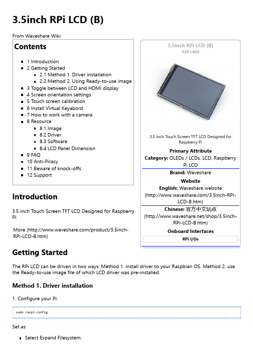
320×480Boot Option -> Desktop Autologin (may differ depending on Raspbian revision)2. Copy the driver (choose the driver according to your OS) into your OS then Run the following commands:tar xvf LCD-show-*.tar.gzcd LCD-show/Install the driver and it toggles the mode to LCD display: Note: Net work connection is required while installing driver to your Pi, or else the touch won't work properly.chmod +x LCD35B-show./LCD35B-showNote: this LCD won't work after apt-get upgrade, in such cases, please edit the config.txt file in the SD card and remove this statement: dtoverlay=ads78463. After system rebooting, the RPi LCD is ready to use.Method 2. Using Ready-to-use imageThe image file with pre-installed driver is located in the IMAGE directory of the CD, or you can download it from #Image. Extract the .7z file and you will get an .img file. Write the image to your micro SD card (How to write an image to a micro SD card for your Pi? See RPi Image Installation Guides for more details). Then insert the card to your Pi, power up and enjoy it.Toggle between LCD and HDMI displayOnce this LCD is enabled, meanwhile the default settings for HDMI are changed. If you want to use another HDMI monitor, please run the following command:cd LCD-show/./LCD-hdmiThis toggles the mode to LCD display:./LCD35B-showScreen orientation settingsAfter touch driver installed, the screen orientation can be set by these commands:0 degree rotationcd LCD-show/./LCD35B-show 090 degree rotationcd LCD-show/./LCD35B-show 90180 degree rotationcd LCD-show/./LCD35B-show 180270 degree rotationcd LCD-show/./LCD35B-show 270Touch screen calibrationThis LCD can be calibrated using a program called xinput_calibrator which is pre-installed on the CD image. However, it was not pre-installed on original Raspbian OS. So in this case, you should get and install the program manually withsudo apt-get install -y xinput-calibratorEnter the following commands for touch screen calibration:sudo DISPLAY=:0.0 xinput_calibratoror select Menu -> Preferences -> Calibrate Touchscreen.After running these commands, there will be a prompt for four-point calibration shown in the LCD screen. Click the points one by one to finish the touch calibration. Then, the new calibration data will be displayed in the terminal, as shows below. Please get these data for future use.Doing dynamic recalibration:Setting new calibration data: 3919, 208, 236, 3913Enter the following command to edit 99-calibration.conf:sudo nano /etc/X11/xorg.conf.d/99-calibration.confThen, the old calibration data will be displayed in the terminal:Section "InputClass"Identifier "calibration"MatchProduct "ADS7846 Touchscreen"Option "Calibration" "160 3723 3896 181"Option "SwapAxes" "1"EndSectionModify the calibration data to the new calibration data displayed above):Section "InputClass"Identifier "calibration"MatchProduct "ADS7846 Touchscreen"Option "Calibration" "3919 208 236 3913"Option "SwapAxes" "1"EndSectionPress the keys Ctrl+X, and select the option Y to save the modification.The modification will be valid after rebooting the system. Enter the following command for system reboot:sudo rebootNotices: In case of inaccurate touch, please perform screen calibration again and reboot the system.Install Virtual Keyabord1. Install matchbox-keyboardsudo apt-get install updatesudo apt-get install matchbox-keyboardsudo nano /usr/bin/toggle-matchbox-keyboard.sh2. Copy the statements below to toggle-matchbox-keyboard.sh and save.#!/bin/bash#This script toggle the virtual keyboardPID=`pidof matchbox-keyboard`if [ ! -e $PID ]; thenkillall matchbox-keyboardelsematchbox-keyboard -s 50 extended&fi3. Execute the commands:sudo chmod +x /usr/bin/toggle-matchbox-keyboard.shsudo mkdir /usr/local/share/applicationssudo nano /usr/local/share/applications/toggle-matchbox-keyboard.desktop4. Copy the statements to toggle-matchbox-keyboard.desktop and save.[Desktop Entry]Name=Toggle Matchbox KeyboardComment=Toggle Matchbox Keyboard`Exec=toggle-matchbox-keyboard.shType=ApplicationIcon=matchbox-keyboard.pngCategories=Panel;Utility;MBX-MB-INPUT-MECHANSIM=True5. Execute commands as below. Note that you need to use "Pi " user permission instead of root to execute this commandnano ~/.config/lxpanel/LXDE-pi/panels/panel6. Find the statement which is similar to below: (It maybe different in different version)Plugin {type = launchbarConfig {Button {id=lxde-screenlock.desktop}Button {id=lxde-logout.desktop}}7. Append these statements to add an button option:Button {id=/usr/local/share/applications/toggle-matchbox-keyboard.desktop}8. reboot your Raspberry Pi. If the virtual keyboard is installed correctly, you can find that there is a keyboard icon on the left of the barsudo rebootHow to work with a camera1. Select "Enable Camera" -> "<YES>"sudo raspi-config2. Copy the Camera driver to the OS of Pi then:unzip camera.zipcd camerasudo chmod 777 Camerasudo cp update\ camera/95-stmpe.rules /etc/udev/rules.d/3. Create a file called wheezy.list.sudo nano /etc/apt/sources.list.d/wheezy.listAppend:deb /raspbian wheezy mainExit with save.4. Create a file called 10defaultRelease.sudo nano /etc/apt/apt.conf.d/10defaultReleaseAppend:APT::Default-release \"stable";Exit with save.5. Create a file called libsdl.sudo nano /etc/apt/preferences.d/libsdlAppend:Package: libsdl1.2debianPin: release n=jessiePin-Priority: -10Package: libsdl1.2debianPin: release n=wheezyPin-Priority: 900Exit with save.6. Last, execute the commands:sudo apt-get updatesudo apt-get -y --force-yes install libsdl1.2debian/wheezysudo apt-get install evtest tslib libts-bin xinputsudo apt-get install python-pipsudo apt-get install python2.7-devsudo pip install picamera==1.10sudo rebootsudo TSLIB_FBDEVICE=/dev/fb1 TSLIB_TSDEVICE=/dev/input/touchscreen ts_calibrateCamera will be enabled by the steps above.ResourceUser manual (/w/upload/3/3e/RPi-LCD-User-Manual.pdf) ImageDescription: if you felt hard to install driver, try the image with driver pre-installed.[Collapse][Collapse]LCD35B-161122.7z (https:///open?id=0BxFRtACVZx9fNlhjMVN5SDVERW8)DriverIf the touch screen doesn't work properly, please install the driver: LCD-show-170703.tar.gz, but not LCD-show-161112.tar.gz.LCD-show-170703.tar.gz (network connection is required while installing)(/w/upload/0/00/LCD-show-170703.tar.gz)LCD-show-161112.tar.gz (/w/upload/4/4b/LCD-show-161112.tar.gz)SoftwarePanasonic SDFormatter (/w/upload/d/d7/Panasonic_SDFormatter.zip)Win32DiskImager (/w/upload/7/76/Win32DiskImager.zip)PuTTY (/w/upload/5/56/Putty.zip)LCD Panel Dimension3.5inch RPi LCD (B) panel dimension (/w/upload/2/2f/3.5inch-rpi-lcd-b-panel-dimension.pdf)FAQQuestion:Why does the touchscreen not work well?Answer:Now, we only provide touch screen drivers for Raspbian and Ubuntu Mate. How to install the driver? See:#Method_1._Driver_installationQuestion:Why does the image in the CD not work on my Pi?Answer:The image in the CD may differ depending on batches, however, some Images are just available for Pi 2 (or before, but not for Pi 3). In such cases you can download the latest version from Raspberry Pi website (https:///downloads/raspbian/) and install the driver. See:#Method_1._Driver_installationMake sure the hardware connection is correct and connects fine.Make sure you've written the image to your SD card using the software File:Win32DiskImager.zip rather then just copy and paste.It is strongly recommended to use a stand-alone 5V/2A power adapter, because the USB port of PC might not have enough power to support the Pi and LCD.。
3.5液晶屏使用说明书
wwwmzdesigncomcnmzdesignmzdesigncomcn2图11模块接口示意图表11模块接口引脚说明接口引脚说明vcc模块供电电源输入一般无特殊要求为5vd0d78位数据总线cs片选低电平有效rstreset复位低电平复位a0控制寄存器数据寄存器选择低电平选择控制寄存器we写信号低电平有效rd读信号低电平有效gnd接地scs预留有ads7846的片选ssck预留有ads7846的spi时钟输入ssdo预留有ads7846的spi数据输出ssdi预留有ads7846的spi数据输入sint预留有ads7846的int信号sbusy预留有ads7846的busy信号mzt35c1模块编程手册北京铭正同创科技有限公司http
动态显示区
70.08×52.56
mm
象素成份
a-Si TFT
LCD 模式
65K TFT
16 位色深度
总线
8 位 Intel 80 总线
背光
白色 LED
由指令控制
Riverdi 3.5英寸 TFT 显示屏参考手册说明书

ITEMCONTENTSUNITLCD Type TFT/Transmissive/Normally white / Size3.5Inch Viewing Direction12:00 (without image inversion) O’ Clock Gray Scale Inversion Direction 6:00O’ Clock Number of Dots 320 x (RGB) × 240 / Driver ICBT81x / Interface TypeSPI/QSPI/ Module Memory Size 1 MB (BT81x) + 64 Mb (external flash) / Color Depth16.7M/ Pixel Arrangement RGB Vertical Stripe/ Surface Treatment Anti-glare / Clear (for CTP) / Input Voltage3.3V3.5” EVE3 SERIES LCD TFTRiTFT-35 seriesRev.1.0 2018-10-22L C D T F T M o d u l e S p e c i f i c a t i o nNote 1: RoHS, REACH SVHC compliant Note 2: LCM weight tolerance: ± 5%.CONTENTS (2)1 MODULE CLASSIFICATION INFORMATION (3)2 ASSEMBLY GUIDE - INTEGRATION (3)2.1 Mounting frame (4)3 MODULE DRAWING (4)4 ABSOLUTE MAXIMUM RATINGS (5)5 ELECTRICAL CHARACTERISTICS (5)6 BACKLIGHT CHARACTERISTICS (5)7 ELECTRO-OPTICAL CHARACTERISTICS (5)8 INTERFACE DESCRIPTION (7)9 BT8x CONTROLLER SPECIFICATIONS (8)9.1 Serial host interface (8)9.2 Block Diagram (8)9.3 Host interface SPI mode 0 (9)9.4 Backlight driver block diagram (9)10 LCD TIMING CHARACTERISTICS (9)10.1 Clock and data input time diagram (9)10.2 Parallel RGB timing table (11)11 TOUCH SCREEN PANEL SPECIFICATIONS (11)11.1 Electrical characteristics (11)11.1.1 For capacitive touch panel (11)11.1.2 For resistive touch panel (12)11.2 Mechanical characteristics (12)11.2.1 For capacitive touch panel (12)11.2.2 For resistive touch panel (13)12 INSPECTION (13)12.1 Inspection condition (13)12.2 Inspection standard (14)13 RELIABILITY TEST (17)14 LEGAL INFORMATION (18)1. BRAND RV – Riverdi2. PRODUCT TYPE T – TFT StandardF – TFT Custom3. DISPLAY SIZE 35– 3.5”4. MODEL SERIAL NO. A (A-Z)5. RESOLUTION H– 320x240 px6. INTERFACE B – TFT + Controller BT81x7. FRAME N – No FrameF – Mounting Frame8. BACKLIGHT TYPE W – LED White9. TOUCH PANEL N – No Touch PanelR – Resistive Touch Panel C – Capacitive Touch Panel10. VERSION 00(00-99)RiTFT-35-RES RVT35AHBNWR00 BT816, resistive touch panelRiTFT-35-CAP RVT35AHBNWC00 BT815, capacitive touch panelRiTFT-35-FR RVT35AHBFWN00 BT816, no touch panel, mounting frame RiTFT-35-RES-FR RVT35AHBFWR00 BT816, resistive touch panel, mounting frame RiTFT-35-CAP-FR RVT35AHBFWC00 BT815, capacitive touch panel, mounting frame2.1Mounting frameFor dimension s 3.5”, 4.3”, 5.0” and 7.0” the product with mounting frame version is available. Thanks to the four catches attached to the side, frame provides strong assembly to the surface by mounting element (like the screw, see Figure 3). The frames are specially designed to fit Riverdi products perfectly. The diameter of the mounting hole is 3.5mm.Figure 1. Mounting frameRiTFT-35 series3MODULE DRAWING `` RiTFT-35© 2018 Riverdi Page 4 of 24 RiTFT-35 seriesRiTFT-35-FR© 2018 Riverdi Page 5 of 24 RiTFT-35 seriesRiTFT-35-CAP© 2018 Riverdi Page 6 of 24 RiTFT-35-CAP-FR© 2018 Riverdi Page 7 of 24 RiTFT-35-RES© 2018 Riverdi Page 8 of 24 RiTFT-35-RES-FR© 2018 Riverdi Page 9 of 24 4ABSOLUTE MAXIMUM RATINGSPARAMETER SYMBOL MIN MAX UNITSupply Voltage for Logic VDD 0 4.0 V Supply Voltage for LED Inverter BLVDD 0 7.0 VInput Voltage for Logic VIN 0 4.0 VLED forward current (each LED) IF - 25 mA Operating Temperature T OP-20 70 °C PARAMETER SYMBOL MIN TYP MAX UNIT NOTES Supply Voltage For Module VDD 3.0 3.3 3.6 VInput Voltage for LED Inverter BLVDD 2.8 5.0 5.5 VLED Backlight Current IDD backlight- 150 187 mA BLVDD=3.3V LED Backlight Current IDD backlight- 93 117 mA BLVDD=5V Input Voltage ' H ' level V IH0.7VDD - VDD VInput Voltage ' L ' level V IL0 - 0.2VDD VInput Current I In TBD mAInput Current for module with CTP I InC TBD mAITEM SYMBOL MIN TYP MAX UNIT Voltage for LED backlight V l- 19.2 20.4 V Current for LED backlight I l- 20 25 mA LED Life Time - 30000 50000 - HrsLNote 1. Contrast Ratio(CR) is defined mathematically as below, for more information see Figure .Contrast Ratio =Average Surface Luminance with all white pixels (P1,P2,P3,P4,P5) Average Surface Luminance with all black pixels (P1,P2,P3,P4,P5)Note 2. Surface luminance is the LCD surface from the surface with all pixels displaying white. For more information, see Figure .Lv = Average Surface Luminance with all white pixels (P1, P2, P3, P4, P5)Note 3.The uniformity in surface luminance δ WHITE is determined by measuring luminance at each test position 1 through 5, and then dividing the maximum luminance of 5 points luminance by minimum luminance of 5 points luminance. For more information, see Figure .δ WHITE =Minimum Surface Luminance with all white pixels (P1,P2,P3,P4,P5) Maximum Surface Luminance with all white pixels (P1,P2,P3,P4,P5)Note 4. Response time is the time required for the display to transition from white to black (Rise Time, Tr) and from black to white (Decay Time, Tf). For additional information see FIG 1. The test equipment is Autronic-Melchers’s ConoScope series.Note 5.CIE (x, y) chromaticity, the x, y value is determined by measuring luminance at each test position 1 through 5, and then make average value.Note 6. Viewing angle is the angle at which the contrast ratio is greater than 2. For TFT module the contrast ratio is greater than 10. The angles are determined for the horizontal or x axis and the vertical or y axis with respect to the z axis which is normal to the LCD surface. For more information see Figure .Note 7. For viewing angle and response time testing, the testing data is based on Autronic-Melchers’s ConoScope series. Instruments for Contrast Ratio, Surface Luminance, Luminance Uniformity, CIE the test data is based on TOPCON’s BM-5 photo detector.Note 8. For TFT module, Gray scale reverse occurs in the direction of panel viewing angle.Figure 2. The definition of response timeFigure 3. Measuring method for Contrast ratio, surface luminance, Luminance uniformity, CIE (x, y) chromaticityFigure 4.The definition of viewing angle8INTERFACE DESCRIPTION9BT8x CONTROLLER SPECIFICATIONSBT8x or EVE3 (Embedded Video Engine 3) simplifies the system architecture for advanced human machine interfaces (HMIs) by providing functionality for display, audio, and touch as well as an object oriented architecture approach that extends from display creation to the rendering of the graphics.9.1Serial host interfaceFigure 5.SPI interface connection Figure 6. QSPI interface connectionSPI Interface– the SPI slave interface operates up to 30MHz.Only SPI mode 0 is supported. The SPI interface is selected by default (MODE pin is internally pulled low by 47k resistor).9.2Block DiagramFigure 7.. BT8x Block diagram9.3Host interface SPI mode 0Figure 8. SPI timing diagramFor more information about BT8x controller please go to official BT8x website.https:///Products/ICs/BT81X.html9.4Backlight driver block diagramBacklight enable signal is internally connected to BT8x Backlight control pin. This pin is controlled by two BT8x’s registers. One of them specifies the PWM output frequency, second one specifies the duty cycle. Refer to BT8x datasheet for more information.Figure 9. Backlight driver block diagram10LCD TIMING CHARACTERISTICS10.1Clock and data input time diagramFigure 10. DE mode timing diagramBT8xFigure 11. SYNC mode timing diagramFigure 12. Timing diagram10.2Parallel RGB timing tableTiming parameter (VDD=3.3V, GND=0V, Ta=25˚C)PARAMETER SYMBOL MIN TYP MAX UNIT CONDITION CLK Clock Time T clk 1/Max(F CLK) - 1/Min(F CLK) ns -11TOUCH SCREEN PANEL SPECIFICATIONS11.1Electrical characteristicsNote: Avoid operating with hard or sharp material such as a ball point pen or a mechanical pencil except a polyacetal pen (tip R0.8mm or less) or a fingerITEM VALUE UNIT REMARKMin. Typ. Max.Linearity - - 1.5 % Analog X and Y directions Terminal Resistance 200 - 900 ΩX100 - 600 ΩY11.2Mechanical characteristicsNote 1: Force test condition, Input DC 5V on X direction, Drop off Polyacetal Stylus (R0.8), until output voltage stabilize, then get the R8.0mm Silicon rubber and do finger Activation force test. Next step, 9 points.Note 2: Measurement surface area conditions, Scratch 100,000 times straight line on the film with a stylus change every 20,000 times with Force: 250gf, Speed: 60mm/sec by R0.8 polaceteal stylus.Note 3: Pitting test, Pit 1, 000, 000 times on the film with R0.8 silicon rubber with Force: 250gf and Speed: 2 times/sec.Note 1: Force test condition, Input DC 5V on X direction, drop off Polyacetal Stylus (R0.8), until output voltage stabilize, then get the R8.0mm Silicon rubber and do finger Activation force test. Next step, 9 points.ITEM VALUE UNIT REMARKMin. Typ. Max.12INSPECTIONStandard acceptance/rejection criteria for TFT module.12.1Inspection conditionAmbient conditions:•Temperature: 25±°C•Humidity: (60±10) %RH•Illumination: Single fluorescent lamp non-directive (300 to 700 lux)Viewing distance:35±5cm between inspector bare eye and LCD.Viewing Angle:U/D: 45°/45°, L/R 45°/45°12.2Inspection standard Item Criterion Black spots, whitespots, light leakage,Foreign Particle(round Type)D=(x+y)2*Spots density: 10 mmSize < 5”Average Diameter Qualified QtyD < 0.2 mm Ignored0.2 mm < D < 0.3 mm 30.3 mm < D < 0.5 mm 20.5 mm < D 0Size >= 5”Average Diameter Qualified Qty D<0.2 mm Ignored0.2 mm < D < 0.3 mm 40.3 mm < D < 0.5 mm 20.5 mm < D 0Clear spotsSize >= 5”Average Diameter Qualified Qty D<0.2 mmIgnored 0.2 mm < D < 0.3 mm 4 0.3 mm < D < 0.5 mm 2 0.5 mm < D*Spots density: 10 mm Size < 5”Average Diameter Qualified Qty D < 0.2 mmIgnored 0.2 mm < D < 0.3 mm 3 0.3 mm < D < 0.5 mm 2 0.5 mm < D 0Polarizer bubblesSize < 5”Average Diameter Qualified Qty D < 0.2 mmIgnored 0.2 mm < D < 0.5 mm 3 0.5 mm < D < 1 mm 2 1 mm < D 0 Total Q’ty 3Size >= 5”Average Diameter Qualified Qty D<0.25 mmIgnored 0.25 mm < D < 0.5 mm 3 0.5 mm < D 0Electrical Dot DefectSize < 5”itemQualified Qty Black do defect 4 Bright dot defect 2 Total Dot 5Size >= 5”itemQualified Qty Black do defect 5 Bright dot defect 2 Total Dot 5Touch panel spotSize < 5”Average Diameter Qualified QtyD < 0.2 mm Ignored0.2 mm < D < 0.4 mm 50.4 mm < D < 0.5 mm 213RELIABILITY TESTNO. TEST ITEM TEST CONDITION REMARKS1 High Temperature Storage 80±2°C/240hours Note 22 Low Temperature Storage -30±2°C/240hours Note 1,2Note 1: Without water condensation.Note 2:The function test shall be conducted after 2 hours storage at the room temperature and humidity after removed from the test chamber.14LEGAL INFORMATIONRiverdi makes no warranty, either expressed or implied with respect to any product, and specifically disclaims all other warranties, including, without limitation, warranties for merchantability, non-infringement and fitness for any particular purpose. Information about device are the property of Riverdi and may be the subject of patents pending or granted. It is not allowed to copy or disclosed this document without prior written permission.Riverdi endeavors to ensure that the all contained information in this document are correct but does not accept liability for any error or omission. Riverdi products are in developing process and published information may be not up to date. Riverdi reserves the right to update and makes changes to Specifications or written material without prior notice at any time. It is important to check the current position with Riverdi.Images and graphics used in this document are only for illustrative the purpose. All images and graphics are possible to be displayed on the range products of Riverdi, however the quality may vary. Riverdi is no liable to the buyer or to any third part for any indirect, incidental, special, consequential, punitive or exemplary damages (including without limitation lost profits, lost savings, or loss of business opportunity) relating to any product, service provided or to be provided by Riverdi, or the use or inability to use the same, even if Riverdi has been advised of the possibility of such damages.Riverdi products are not fault tolerant nor designed, manufactured or intended for use or resale as on line control equipment in hazardous environments requiring fail – safe performance, such as in the operation of nuclear facilities, aircraft navigation or communication systems, air traffic control, direct life support machines or weapons systems in which the failure of the product could lead directly to death, personal injury or severe physical or environmental damage (‘High Risk Activities’). Riverdi and its suppliers specifically disclaim any expressed or implied warranty of fitness for High Risk Activities. Using Riverdi products and devices in 'High Risk Activities' and in any other application is entirely at the buyer’s risk, and the buyer agrees to defend, indemnify and hold harmless Riverdi from any and all damages, claims or expenses resulting from such use. No licenses are conveyed, implicitly or otherwise, under any Riverdi intellectual property rights.。
PT035TN01 V.3 innolux3.5数字屏规格书
I NNO L U XInnoLux copyright 2004All rights reserved,Copying forbidden.Record of RevisionVersion Revise Date Page Content1 2006/3/10 Initial releaseI NNO L U XContents:1. General Specifications (1)2. Pin Assignment (2)3. Operation Specifications (5)3.1. Absolute Maximum Rating (5)3.2. Power Sequence (6)3.3. Electrical Characteristics (7)3.3.1. Typical Operation Conditions (7)3.3.2. Current Consumption (8)3.3.3. Backlight Driving Condition (8)3.4. Timing Characteristics (9)3.4.1. AC Electrical Characteristics (9)3.4.2. Timing Diagram (12)4. Optical Specifications (15)5. Reliability Test Items (19)6. Handling Precautions (20)6.1. Safety (20)6.2. Handling (20)6.3. Static Electricity (20)6.4. Storage (20)6.5. Cleaning (20)7. Mechanical Drawing (21)8. Package Drawing (22)8.1. Packaging Material Table (22)8.2. Packaging Quantity (22)8.3. Packaging Drawing (23)1. General SpecificationsNo. Item Specification Remark1 LCD size 3.5” inch2 Driver element a-Si TFT active matrix3 Resolution 320X3(RGB)X2404 Display mode Normally White, Transmissive with Micro Reflective5 Dot pitch 0.073(W)X0.219(H) mm6 Active area 70.08(W)X52.56(H) mm7 Module size 78.2(W)X65.0(H)X3.5(D) mm Note 18 Surface treatment Hard coating9 Color arrangement RGB-stripe10 Interface Digital11 Backlight power consumption 0.396W(Typ.)12 Panel power consumption 20mW(Typ.)13 Weight 35gNote 1: Refer to Mechanical Drawing.2. Pin AssignmentPin No. Symbol I/O Function Remark1 GLED P GND for LED2 GLED P GND for LED3 VLED P Power for LED4 VLED P Power for LED5 GND P Ground6 NC I No connect7 NC I No connect8 NC I No connect9 NC I No connect10 GND P Ground11 NC - No connect12 NC - No connect13 POL O Polarity select for the line inversion control signal.14 RESET I Reset15 SPENA I Serial port data enable signal. Normally pull high.16 SPCK I Serial port clock .Normally pull high.17 SPDA I/O Serial port data input/output.18 D00 I Data 00 Note219 D01 I Data 01 Note220 D02 I Data 02Note221 D03 I Data 03Note222 D04 I Data 04Note223 D05 I Data 05Note224 D06 I Data 06Note225 D07 I Data 07Note226 D08 I Data 08Note227 D09 I Data 09Note228 D10 I Data 10Note229 D11 I Data 11Note230 D12 I Data 12Note231 D13 I Data 13Note232 D14I Data 14Note233 D15I Data 15Note234 D16I Data 16Note235 D17I Data 17Note236 D18I Data 18Note237 D19I Data 19Note238 D20I Data 20Note239 D21I Data 21Note240 D22I Data 22Note241 D23I Data 23Note242 IHS I Horizontal synchronous signal43 IVS I Vertical synchronous signal44 CLK I Data clock45 AV DD P Analog power supply(+5V)46 AV DD P Analog power supply(+5V)47 V CC P Digital power supply(+3.3V)48 V CC P Digital power supply(+3.3V)49 NC - No connect50 V GL I Negative power for scan driver51 V GL I Negative power for scan driver52 NC - No connect53 V GH I Positive power for scan driver54 NC - No connect55 NC - No connect56 V COM I V COM input57 V COM I V COM input58 DEN I Data enabling signal59 GND P Ground60 GND P GroundNote1: P - PowerI - InputO -OutputNote 2 :Mode D[23:16] D[15:8] D[7:0] IHS IVS DENITU-R BT 656 D[23:16]GND GND NC NC NCITU-R BT 601 D[23:16]GND GND IHS IVS NCNC for HV Mode8 bit RGB D[23:16]GND GND IHS IVSDEN for DEN ModeNC for HV Mode 24 bit RGB R[7:0] G[7:0] B[7:0]IHS IVSDEN for DEN Mode3. Operation Specifications3.1. Absolute Maximum Rating(GND =0V, Note 1)ValuesItem SymbolUnit RemarkMin. Max.V CC -0.3 7 VAV DD -0.3 7 V Power voltageV GH -0.3 18 VV GL -15 0.3 VV GH-V GL- 33 V Operation Temperature T OP -30 85 ℃Storage Temperature T ST -30 85 ℃Note 1: Device is subject to be damaged permanently if stresses beyond those absolute maximum ratings listed above.3.2. Power Sequence3.2.1 Power on:3.2.2 Power off:3.3. Electrical Characteristics3.3.1. Typical Operation Conditions(GND =0V, Note 2)ValuesUnit Remark Item SymbolMin. Typ. Max.V CC 3.0 3.3 3.6 VAV DD 4.8 5.0 5.2 VPower voltageV GH 14.3 15 15.7 VV GL -10.5 -10 -9.5 VV CAC - 5.0 - V Note 1V COMV CDC 1.29 1.49 1.69 VInput logic high voltage V IH 0.7V CC - V CC VInput logic low voltage V IL 0 - 0.3V CC VNote 1: The brightness of LCD panel could be changed by adjusting the AC component of V COM.Note 2: Be sure to apply GND, V CC, and V GL, to the LCD first, and then apply V GH.3.3.2. Current Consumption(GND =0V)ValuesUnit Remark Item SymbolMin. Typ. Max.I GH - 100 300 uA V GH =+15VI GL - -100 -300 uA V GL = -10V Current for DriverI CC - 1.3 5 mA V CC =3.3VI DD - 2 5 mA AV DD =5V3.3.3. Backlight Driving ConditionValuesUnit Remark Item SymbolMin. Typ. Max.LED voltage V L - 19.8 - V Note 1LED current I L - 20 - mA Note 1LED life time - 20,000 - - Hr Note 2Note 1: The LED driving condition is defined for each LED module. (See the figure)Note 2: The “LED life time” is defined as the module brightness decrease to 50% original brightness that the ambient temperature is 25℃ and I L =20mA.3.4. Timing Characteristics3.4.1. AC Electrical Characteristics3.3.1.1 AC Electrical Characteristics(VCC=3.3V,AVDD=5.0V, GND=AGND=0V,TA=25℃)ValuesItem SymbolMin. Typ. Max.Unit. RemarkSystem Operation TimingVDD power on slew time T POR 1000 us From 0V to 90%VDDInput Output TimingCLKIN clock time Tclk - 37 ns HSD to CLKIN Thc - - 1 Tclk HSD width Thwh 1 - - Tclk VSD width Tvwh 1 - - Th HSD period time Th 60 63.56 67 us VSD setup time Tvst 12 - - ns VSD hold time Tvhd 12 - - ns HSD setup time Thst 12 - - nsData set-up time Tdsu 12 - - ns DIN[7:0] to CLKINData hold time Tdhd 12 - - ns DIN[7:0] to CLKINDEN setup time Tesd 12 - - ns DEN to CLKINVCOMOUT output stable time Tcst - 4 8 us96% final,CLcom=33nF,RLcom=100ohm3.3.1.2 Timing TableITU-R BT 601 Mode A/B*(Note 1)ValueUnit Remark ITEM SymbolMin. Typ. Max.CLKIN frequency Fclk - 24.54/27 30 Mhz VCC=3.3V CLKIN cycle time Tclk - 40/37 - nsCLKIN pulse duty Tcwh 40 50 60 % Tclk ITU-R BT 656 Mode A/B*(Note 1)ValueUnit Remark ITEM SymbolMin. Typ. Max.CLKIN frequency Fclk - 27 30 Mhz VCC=3.3V CLKIN cycle time Tclk - 37 - nsCLKIN pulse duty Tcwh 40 50 60 % Tclk8 bit RGB 960x240 ModeValueUnit Remark ITEM SymbolMin. Typ. Max.CLKIN frequency Fclk - 27 30 Mhz VCC=3.3V CLKIN cycle time Tclk - 37 - nsCLKIN pulse duty Tcwh 40 50 60 % TclkNote 1: YUV mode A: Data sequence are ”Cb-Y-Cr-Y…”YUV mode B: Data sequence are ”Cr-Y-Cb-Y…”24 Bit RGB 960 CH Mode (320(RGB) x 240)ValuesItem SymbolMin. Typ. Max.Unit. Remark CLKIN frequency F clk- - 27 Mhz VDD=3.0~3.6V CLKIN cycle time T clk- - 37 nsCLKIN pulse duty T cwh40 50 60 % T clkTime from HSD to STV T hstv- 3 - TclkTime from HSD to LD T hld- 24 - TclkTime from HSD to CKV T hckv- 20 - TclkTime from HSD to OEV T hoev- 10 - TclkTime from HSD to VCOMOUT T hvcm- 40 - Tclk LD falling Time from HSD to DATSEQ T hseq- 20 - TclkLD pulse width T wld- 16 - TclkCKV pulse width T wckv- 40 - TclkOEV pulse width T woev- 40 - TclkTime that HSD to 1’st data input Ths 24 70 255 TclkDDLY=70, offset=0(fixed)3.3.1.33-wire serial communication AC timingValuesItem SymbolMin. Typ. Max.Unit. Remark Serial Clock Period Time Tspck 320 - - nsSPCK pulse duty cycle Tscdut 40 50 60 %Serial data setup time Tisu 120 - - nsSerial data hold time Tihd 120 - - nsSerial clock high/low Tssw 120 - - nsSPENAselect distinguishTcd 1 - - us3.4.2.Timing DiagramInput Data Timing1. Clock and Data Input Timing DiagramCLKINDIN[7:0]HSD2. 8 bit RGB input Data format3. ITU-R BT 6015. 24 bit RGB mode for 960 x 2403-Wire Timing DiagramNote: 3-Wire Control Registers List3-Wire Register Register DescriptionD[15:10] Name Init R/W Function Description000000b R00 (03h) R/W System control register000001b R01 (40h) R/W Timing controller function register 000010b R02 (11h) R/W Operation control register000011b R03 (cch)*R/W Input data format control register 000100b R04 (93h) R/W Source Timing delay control register 000101b R05 (12h) R/W Gate Timing delay control register 000111b R07 (03h) R/W Internal function control register 001000b R08 (08h) R/W RGB contrast control register001001b R09 (40h) R/W RGB brightness control register 001010b R0A (88h) R/W Hue/Saturation control register001011b R0B (88h) R/W R/B Sub-contrast control register 001100b R0C (20h) R/W R Sub-brightness control register 001101b R0D (20h) R/W B Sub-brightness control register* Note: c4h:ITU-R BT 656 Modec2h:ITU-R BT 601 Modec8h:8 bit RGB Mode(HV Mode)c9h:8 bit RGB Mode(DE Mode)cch:24 bit RGB Mode (HV mode)cdh:24 bit RGB Mode (DE mode)4. Optical SpecificationsItemSymbol ConditionMin.Typ. Max. UnitRemarkθLΦ=180°(9 o’clock) 55 65 - θR Φ=0°(3 o’clock)5565 -θT Φ=90°(12 o’clock) 35 45 - Viewing angle (CR≥10)θB Φ=270°(6 o’clock) 5565 - degreeNote 1T ON-1530msecNote 3 Response TimeT OFF- 20 50 msec Note 3 Contrast ratioCR 200 300-- Note 4 W X- (0.33) - - Color chromaticityW Y- (0.36) - - Note 5 Note 6 LuminanceL300 350 - cd/m ² Note 6 Luminance uniformity Y UNormal θ=Φ=0°7075-%Note 7Test Conditions:1. V CC =3.3V, AV DD =5.0V, I L =20mA (Backlight current), the ambient temperature is 25℃.2. The test systems refer to Note 2.Fig. 5-1 Definition of viewing angleNote 2: Definition of optical measurement system.The optical characteristics should be measured in dark room. The opticalproperties are measured at the center point of the LCD screen. (Response time ismeasured by Photo detector TOPCON BM-7, other items are measured by BM-5A/Field of view: 1° /Height: 500mm.)Fig. 5-2 Optical measurement system setupΦ=0°Note 3: Definition of Response timeThe response time is defined as the LCD optical switching time interval between“White” state and “Black” state. Rise time (T ON ) is the time between photo detector output intensity changed from 90% to 10%. And fall time (T OFF ) is the time between photo detector output intensity changed from 10% to 90%.Fig. 5-3 Definition of response timeNote 4: Definition of contrast ratiostateBlack"" the on is LCD when measured Luminance stateWhite"" the on is LCD when measured Luminance =(CR) ratio ContrastNote 5: Definition of color chromaticity (CIE1931)Color coordinates measured at center point of LCD.Note 6: All input terminals LCD panel must be ground when measuring the center area ofthe panel.90%10% 0%Photo detector output (Relative value)ONWhite (TFT OFF)Black (TFT ON)White (TFT OFF)Note 7: Definition of Luminance UniformityTo test for uniformity, the tested area, which is inside the active area, isdivided into 3 rows and 3 columns. The measurement spot is placed at the center of each box.max minB B (Yu)Uniformity Luminance =L-------Active area length W----- Active area widthFig. 5-4 Definition of uniformityB max : The measured maximum luminance of all measurement position. B min : The measured minimum luminance of all measurement position.5. Reliability Test ItemsItem Test Conditions Remark High Temperature Storage Ta = 85℃240 hrs Note 1 Low Temperature Storage Ta = -30℃240hrs Note 1 High Temperature Operation Ts = 85℃240hrs Note 2 Low Temperature Operation Ta = -30℃240hrs Note 1 Operate at High Temperatureand Humidity+60℃, 90%RH max. 240 hrsThermal Shock -30℃/30 min ~ +85℃/30 min for a total 100 cycles, Start with cold temperature and end with high temperatureVibration Test Frequency range:10~55Hz Stroke:1.5mmSweep:10Hz~55Hz~10Hz2 hours for each direction of X. Y. Z.(6 hours for total)Mechanical Shock 100G 6ms,±X, ±Y, ±Z 3 times for each directionPackage Vibration Test Random Vibration :0.015G*G/Hz from 5-200HZ, -6dB/Octave from 200-500HZ2 hours for each direction of X. Y. Z.(6 hours for total)Package Drop Test Height:60 cm1 corner, 3 edges, 6 surfacesElectro Static Discharge ± 2KV, Human Body Mode, 100pF/1500ΩNote 1: Ta is the ambient temperature of samples.Note 2: Ts is the temperature of panel’s surface.Note 3: In the standard condition, there shall be no practical problem that may affect the display function.6. Handling Precautions6.1. SafetyLiquid crystal is poisonous. Do not put it in your mouth. If liquid crystal touches your skin or clothes, wash it off immediately by using soap and water.6.2. Handling1. The LCD panel is plate glass. Do not subject the panel to mechanical shock or toexcessive force on its surface.2. The polarizer attached to the display is easily damaged. Please handle it carefullyto avoid scratch or other damages.3. To avoid contamination on the display surface, do not touch the module surfacewith bare hands.4. Keep a space so that the LCD panels do not touch other components.5. Put cover board such as acrylic board on the surface of LCD panel to protect panelfrom damages.6. Transparent electrodes may be disconnected if you use the LCD panel underenvironmental conditions where the condensation of dew occurs.7. Do not leave module in direct sunlight to avoid malfunction of the ICs.6.3. Static Electricity1. Be sure to ground module before turning on power or operating module.2. Do not apply voltage which exceeds the absolute maximum rating value.6.4. Storage1. Store the module in a dark room where must keep at +25±10℃ and 65%RH orless.2. Do not store the module in surroundings containing organic solvent or corrosivegas.3. Store the module in an anti-electrostatic container or bag.6.5. Cleaning1. Do not wipe the polarizer with dry cloth. It might cause scratch.2. Only use a soft sloth with IPA to wipe the polarizer, other chemicals mightpermanent damage to the polarizer.7. Mechanical Drawing8. Package Drawing8.1. Packaging Material TableNo Item Model (Material) Dimensions(mm)UnitWeight(Kg)Quantity(pcs)Remark1 LCM module PT035TN01 V.3 78.2 ×65.0 ×3.5 0.0352 2602 Corrugated Board-1BC Corrugated Paper510×343 0.130 23 Corrugated Board-2B Corrugated Paper 1152×512 0.26 14 Corrugated Bar B Corrugated Paper 343×104 0.020 125 Partition BC Corrugated Paper512×343×106 1.045 26 Dust-Proof Bag PE 700×530 0.0604 17 A/S Bag PE 112×90 1.1108×10^-32608 Carton Corrugated Paper 530×355×255 1.1 19 Total weight 13.5± 5% Kg8.2. Packaging Quantity(1) LCM quantity per Partition: 2 row x 21 pcs + 4 row x 22 pcs = 130 pcs(2) Total LCM quantity in Carton: 2 layer x 130 pcs per Partition = 260 pcs8.3. Packaging Drawing。
3.5寸TFT液晶规格书
Contents TFT transmissive, Normally white 6 O’clock 54.66(W)X82.94(H)X2.3(T) 48.96(W) x 73.44(H) 320(H) x (R.G.B.) x480(W) HX8357B 262K LED NC 8080 system 8/16 bit parallel T.B.D.
TEL: 86-0755-23000930 FAX : 86-0755-23000936
Doc No: Rev.:
XC-T0353701 0 2012.03.26
6 of 23
深圳信创光电技术有限公司
SHEN ZHEN SHI SINGSTART OPTOELECTRONIC CO., .,LTD .,
Item Contrast ratio (Center point) Response Rising: Tr Time Falling:Tf White Color Chromaticit y (CIE 1931) Red Green Blue Hor Ver
Symbol C/R Tr Tf Wx Wy Rx Ry Gx Gy Bx By θL1 θR1 øU1 øD1
Min -0.3 -0.3 -10 -20 -
Max 3.3 Vcc+0.3 60 70 90%(Max60°C) 15
Unit V V °C °C Dot mA(each Led)
Doc No: Rev.:
XC-T0353701 0 2012.03.26
8 of 23
深圳信创光电技术有限公司
SHEN ZHEN SHI SINGSTART OPTOELECTRONIC CO., .,LTD .,
天马3.5寸工业液晶屏TM035KDH03规格书-杭州旭虹科技有限公司
杭州旭虹科技有限公司
SHANGHAI TIANMA MICRO-ELECTRONICS TM035KDH03 V1.3
Table of Contents
Coversheet........................................................................................................................................ 1 Record of Revision............................................................................................................................ 3 1. 2. 3 4 5 6 7 8 9 General Specifications ............................................................................................................... 4 Input/Output Terminals ............................................................................................................... 5 Absolute Maximum Ratings ....................................................................................................... 8 Electrical Characteristics............................................................................................................ 8 Timing Chart............................................................................................................................. 10 Optical Characteristics ............................................................................................................. 17 Environmental / Reliability Tests............................................................................................... 21 Mechanical Drawing................................................................................................................. 22 Packing drawing ...................................................................................................................... 23
3.5寸彩色TFT液晶屏单片机接口-S035Q08-T
Check
Engineering Date Prepared
Characteristics
Mechanical
1. 8/ 9/ 16/ 18-bit 6800-series / 8080-series Parallel Interface 2. Serial Peripheral Interface (SPI) 3. 18-/6-bit RGB interface (DEN, DOTCLK,HSYNC,VSYNC,DB[17:0]) 4. VSYNC interface (system interface + VSYNC) 5. WSYNC interface (system interface + WSYNC) Connect type Connector Color Depth 262K Technology type a-Si Display Spec. Pixel pitch (mm) 0.219 x 0.219 Pixel Configuration R.G.B. Vertical Stripe Display Mode Normally White Driver IC TBD Surface Treatment HC Viewing Direction 6 O’clock LCM (W x H x D) (mm) 76.90*64.0*4.2 Active Area(mm) 70.08 x 52.56 With /Without TSP With TSP Weight (g) TBD LED Numbers 6 LEDs
- 1、下载文档前请自行甄别文档内容的完整性,平台不提供额外的编辑、内容补充、找答案等附加服务。
- 2、"仅部分预览"的文档,不可在线预览部分如存在完整性等问题,可反馈申请退款(可完整预览的文档不适用该条件!)。
- 3、如文档侵犯您的权益,请联系客服反馈,我们会尽快为您处理(人工客服工作时间:9:00-18:30)。
0x01
cmd_write
0xC8
parameters
0x0c
parameters
0x05
parameters
0x0a
parameters
0x6b
parameters
0x04
parameters
0x00
parameters
0x1F
parameters
0x16
parameters
0x00
parameters
* Driving Condition : 320x3Ch-Source / 480Ch-Gate
* Connection
: ZIF Type (45pins,Hirose:FH26-45S-0.3SHW)
* LCD Driver & Control IC : R61581(RENESAS)
* Back Light
0x2A
parameters
0x00
parameters
0x00
parameters
0x01
parameters
0x3F
cmd_write
0x2B
parameters
0x00
parameters
0x00
parameters
0x01
parameters
0xDF
cmd_write
0x35
parameters
Item
Resolution
Main Sub
LCM Outline Demension
Active Area (W × H)
Main Sub
Pixel Pitch (W x H)
Main Sub
Viewing Direction (Human Eye)
Gray Scale Inversion Direction
PRODUCT SPECIFICATION
5. Recommended Software Setting Value (LDI :R61581)
INITIAL CODE
hardware reset
delay 10ms
cmd_write
0xFF
cmd_write
Rev. O
Page All
* Records of Revision *
Description of changes Original Release
Date prepared by 11.08.11 Ruifeng.yang
□ 一般事项 特殊事项内容:
□ 特殊事项
Model
GTB353248-L497L
3/28
PRODUCT SPECIFICATION
1. Features
The features of BTL353248-L497L are as follows
* Display mode : TFT 260K Colors,Transmissive,Normally White
Ta=25℃ Remark
Note 1
Note 2
Note 1) The value can be adjusted by software to optimize display quality Note 2) Display White Pattern
Model
GTB353248-L497L
6/28
parameters
0x14
parameters cmd_write parameters parameters parameters cmd_write parameters parameters parameters cmd_write
0xA2 0xD1 0x03 0x33 0x0a 0xD2 0x03 0x04 0x04 0x29
: White LED Back Light (6 Chips in Serial)
* MPU Interface : CPU Interface, 8-/9-/16-/18-bit Data Bus
* Type of Surface Contion : Clear Type
2. Mechanical Specifications
0xFF
delay 5ms
cmd_write
0xFF
cmd_write
0xFF
cmd_write
0xFF
cmd_write
0xFF
delay 10ms
cmd_write
0xB0
parameters
0x00
cmd_write
0xB3
parameters
0x02
parameters
0x00
parameters
Model
GTB353248-L497L
2/28
PRODUCT SPECIFICATION
* Contents *
1. Features 2. Mechanical Specifications 3. Absolute Maximum Ratings 4. Electrical Characteristics 5. Recommended Software Setting Value (Initial Code) 6. Back Light System Characteristics 7. Optical Characteristics 8. Block Diagram 9. Interface Pin Assignment 10. Power Supply Sequence 11. Read/Write Timing characteristics (80 series MPU) 12. External Dimension 13. LCD Module Numbering System 14. Package Terms 15. LCD Module Out-Going Quality Level 16. Customer Quality Service Process 17. LCD Module Operation Instruction
parameters starty_low_byte
parameters endy_hi_byte
parameters endy_low_byte
cmd_write
0x2C
ENTER SLEEP
cmd_write
0x10
delay 10ms
EXIT SLEEP
cmd_write
0x11
delay 10ms
BLOCK WRITE
cmd_write
0x2A
parameters startx_hi_byte
parameters startx_low_byte
parameters endx_hi_byte
parameters endx_low_byte
cmd_write
0x2B
parameters starty_hi_byte
PRODUCT SPECIFICATION
4. Electrical Characteristics
Main
Items Logic voltage Anolog(Power) voltage Gate High level voltage Low level Input signal High level voltage Low level
0x31
parameters
0x0A
parameters
0x0B
parameters
0x0C
parameters
0x64
parameters
0x0b
parameters
0x0a
parameters
0x05
parameters
0x0c
parameters
0x31
parameters
0x00
cmd_write
LCD Module User Manual
Dalian Good Display Co.,Ltd. LCD Module User Manual GTB353248-L497L
Dalian Good Display Co., Ltd.
Tel: +86-411-84619565 Fax: +86-411-84619585
current consumption
Symbol IOVCC VCC VGH VGL VIH VIL Icc
Min. 1.65 2.72 12 -10 0.8xIOVCC -0.3
-
Typ. 2.8 2.8
18
Max. 3.3 2.88 18 -7 IOVCC 0.2xIOVCC 24
Unit V V V V V V mA
90% RH Max.
Note1 : Device is subject to be damaged permanently, if stresses beyond those absolute maximum ratings listed above.
Model
GTB353248-L497L
5/28
cmd_write
0xD0
parameters
0x07
parameters
0x07
parameters
0x14
parameters
0xA2
cmd_write
0xD1
parameters
0x03
parameters
0x33
parameters
0x0a
delay 10ms