液晶屏规格书系列
3.5寸液晶屏规格书SGC035COM—54PIN
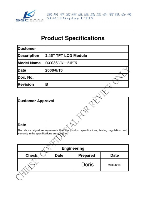
Product SpecificationsCustomerDescription 3.45” TFT LCD ModuleModel Name SGC035COM—54PINDate 2008/6/13Doc. No.Revision BCustomer ApprovalDateThe above signature represents that the product specifications, testing regulation, and warranty in the specifications are acceptedEngineeringCheck Date Prepared DateDoris2008/6/13CONTENTSNo. ITEM PAGE0 RECORD OF REVISION 31 SUMMARY 42 FEATURES 43 GENERAL SPECIFICATIONS 44 ABSOLUTE MAXIMUM RATINGS 45 ELECTRICAL CHARACTERISTICS 56 DC CHARATERISTICS 67 AC CHARACTERISTICS 6~108 OPTICAL CHARATERISTIC 119 TOUCH PANEL 14~1510 INTERFACE 16~1911 BLOCK DIAGRAM 2012 QUALITY ASSURANCE 2113 OUTLINE DRAWING 2214 PACKAGE INFORMATION 2315 PRECAUTIONS 24~26RECORD OF REVISIONSRevision Date Page DescriptionA 2008/2/12 all New CreationB 2008/6/13 18 LCM PIN Definition1. SUMMARYThis technical specification applies to 3.45“color TFT-LCD panel. The 3.45“ color TFT-LCD panel is designed for GPS, camcorder, digital camera application and other electronic products which require high quality flat panel displays. This module follows RoHS.2. FEATURESHigh Resolution: 230,400 Dots (320 RGB x 240). SGC 035COM—54PIN is atransmissive type color active matrix liquid crystal display (LCD) which uses amorphous thin film transistor (TFT) asswitching devices. This product is composed of a TFT LCD panel, driver ICs, FPC, backlight unit and touch panel.,3. GENERAL SPECIFICATIONSParameter Specifications Unit Screen size 3.45(Diagonal) InchDisplay Format 320 RGB x 240 DotActive area 70.08(H) x 52.56(V) mmDot size 73x 219 umPixel Configuration RGB-Stripe Outline dimension 76.9(W) x 63.9(H) x 3.3(D) mm Display Mode Normally white/Transmissive Surface Treatment Haze 20% Display Garmut NTSC 60% Input Interface Digital 24-bit RGB/SERIALRGB/CCIR656/CCIR601Weight (31) g View Angle direction 6 o’clockOperation -20~70 ℃Temperature RangeStorage -30~80 ℃4. ABSOLUTE MAXIMUM RATINGSItem Symbol Condition Min. Max. Unit Remark Power Voltage DVDD,AVDD GND=0 -0.3 5.0 V Input SignalVoltage V in GND=0 -0.3 VDD+0.3 VNOTE Logic OutputVoltageV OUT GND=0 -0.3 VDD+0.3 V NOTENote: Device is subject to be damaged permanently if stresses beyond those absolute maximum ratings listed above1. Temp. ≤ 60℃, 90% RH MAX.Temp. > 60℃, Absolute humidity shall be less than 90% RH at 60℃2.5. ELECTRICAL CHARACTERISTICS 5.1. Operating conditions:Parameter SymbolRatingMin. Typ. Max.Unit ConditionPower Voltage VCC 3.0 3.3 3.6 V Digital Operation CurrentIcc 8.6 mA Gate On Power VGH 14 15 18 V Gate Off Power VGL -11-10 -8V Vcom High Voltage VcomH 3.7 V Note1 Vcom low VoltageVcomL-1.6VNote1Vcom level max VcomA 6 VNote1. VcomH& VcomL :Adjust the color with gamma data. Vp-p should be higher then4V.(Option 5V)Note: Please power on following the sequence VCC Æ VDD5.2 LED driving conditionsParameter Symbol Min. Typ. Max. Unit Remark LED current- 20 - m A Power Consumption - 400 420 mW LED voltage VBL+ 18.619.8 21 V Note 1 LED Life Time - (50,000)- - HrNote 2,3Note 1 : There are 1 Groups LEDILEDNote 2 : Ta = 25℃Note 3 : Brightess to be decreased to 50% of the initial value深圳宏辉成液晶显示有限公司/6. DC CHARATERISTICSParameter SymbolRatingUnit Condition Min. Typ. Max.Low level input voltage V IL 0-0.3VCCVHight level input voltage V IH0.7VCC-VCC V7. AC CHARATERISTICSDigital Parallal RGB interfaceSignal Item Symbol Min Typ Max UnitFrequency Tosc - 156 - ns Dclk High Time Tch - 78 - nsLow Time Tcl - 78 - nsDataSetup Time Tsu 12 - - nsHold Time Thd 12 - - nsPeriod TH - 408 - Tosc Pulse Width THS 5 30 - ToscHsyncBack-Porch Thb 38 ToscDisplay Period TEP - 320 - ToscHsync-den time THE 36 68 88 TsocFront-Porch Thf - 20 - ToscPeriod Tv - 262 - THPulse Width Tvs 1 3 5 TH Vsync Back-Porch Tvb - 15 - TH Display Period Tvd - 240 - THFront-Porch Tvf 2 4 - TH1. Thp + Thb = 68, the user is make up by yourself.2. Tv = Tvs + Tvb + Tvd + Tvf , the user is make up by yourself.3.When SYNC mode is used,1st data start from 68th Dclk after Hsync fallingDigital Serial RGB interfaceSignal Item Symbol Min Typ Max Unit Frequency Tosc - 52 - ns Dclk High Time Tch - 78 - ns Low Time Tcl - 78 - nsData Setup Time Tsu 12 - - nsHold Time Thd 12 - - nsPeriod TH - 1224 - Tosc Pulse Width THS 5 90 - ToscHsyncBack-Porch Thb 114 ToscDisplay Period TEP - 960 - Tosc Hsync-den time THE 108 204 264Front-Porch Thf - 60 - ToscPeriod Tv - 262 - THPulse Width Tvs 1 3 5 THVsync Back-Porch Tvb - 15 - THDisplay Period Tvd - 240 - THFront-Porch Tvf 2 4 - TH Note: 1. Thp + Thb = 204, the user is make up by yourself.2. Tv = Tvs + Tvb + Tvd + Tvf , the user is make up by yourself.3. When SYNC mode is used,1st data start from 204th Dclk after Hsync fallinCCIR601/656 InterfaceSignalData Setup Time Tsu 12 - - ns Hold Time Thd 12 - - ns深圳宏辉成液晶显示有限公司/[_//f+--------------------H " "'= 1560--------------------+jInvalid Data Inva l i d Da t a018,0"'=DOTCLK In va li d DataIn v a l i d Data]---...t--f------------H018, =1440-------------+jslrL//RR[7:0]In va lid DataIn va l i d Dataf---- t.<sP = HBP[6:0]'4+STH[1:0'1-- *. - ----------- IH0,se = 128--- --- ----.!Figure1 CCIR601 Horizontal Timing深圳宏辉成液晶显示有限公司 /手机 : 133 166 766 58 MSN: lcd.sales@ QQ:1378107648Doc. No.SEL[2:0] = 100- 111, NTSCVSYNC HSYNCRR[7:0]tveP = VBP[6:0]DL1DL2DL3IDL2391DL240I---ODD Field VSYNCEVEN FieldHSYNCRR[7:0]tvsP= VBP[6:0] + 1·IODD FieldI IDL1DL2DL3IDL2391DL240ISEL[2:0] = 100- 111, PAL, PALM=OEVEN VSYNCHSYNCRR[7:0]tvsP= VBP[6:0]DL1DL2DL3IDL2791DL280IODD Field VSYNCEVEN Fi l eHSYNCRR[7:0]tvsP= VBP[6:0] + 1·IODD FieldI IDL1DL2DL3IDL2791DL280ISEL[2:0] = 100 - 111, PAL, PALM=1EVEN VSYNCHSYNCRR[7:0]tveP= VBP[6:0]DL1DL2DL3IDL2871DL288 1ODD Field VSYNCEVEN Fi l eHSYNCI深圳宏辉成液晶显示有限公司 /手机 : 133 166 766 58 MSN: lcd.sales@ QQ:1378107648IRR[7:0]lvsP= VBP[6 0] + 1·IDL1DL2DL3IDL287 1DL288 1Figure1CCIR601 Vertical Timing深圳宏辉成液晶显示有限公司 /手机 : 133 166 766 58 MSN: lcd.sales@ QQ:1378107648Figure2 CCIR656 Horizontal Timing深圳宏辉成液晶显示有限公司 /手机 : 133 166 766 58 MSN: lcd.sales@ QQ:1378107648Figure2 CCIR656 Vertical Timing深圳宏辉成液晶显示有限公司 /手机 : 133 166 766 58 MSN: lcd.sales@ QQ:1378107648Figure 3Digital RGB NTSC mode Vertical Data Format for 262THH cycle = 1224tHBP = 204HDISP = 960t HFP = 60DOTCLKHSYNCPixel DataDumm yD0D1----------D 957 D 958 D 959Dum mya ) Horizontal Data Transaction Tim ing V cycle = 262 Lines t VBP = 18VSYNC VDISP = 240 Lines t VFP = 4HSYNC Line 0 b ) Vertical Data Transaction Tim ing Line 239深圳宏辉成液晶显示有限公司 /手机 : 133 166 766 58 MSN: lcd.sales@ QQ:1378107648Figure 3 Data Transaction Timing in Serial RGB (8 bit) Interface (SYNC Mode)深圳宏辉成液晶显示有限公司 /手机 : 133 166 766 58 MSN: lcd.sales@ QQ:1378107648Figure3 Data Transaction Timing in Serial RGB (8 bit) Interface (DE Mode)深圳宏辉成液晶显示有限公司 /手机 : 133 166 766 58 MSN: lcd.sales@ QQ:1378107648Figure3Data Transaction Timing in Parallel RGB (24 bit) Interface (SYNC Mode)深圳宏辉成液晶显示有限公司 /手机 : 133 166 766 58 MSN: lcd.sales@ QQ:1378107648Figure4 Data Transaction Timing in Parallel RGB (24 bit) Interface (DE Mode)7.1.1 Standby ON/OFF Control LQ35NC211 has a power ON/OFF sequence control function. When STB pin is pulled L,blank data is outputted for 5-frames first, form the falling edge of the following VSYNC signal. The blank data would be gray level 255 for normally white LC.Figure5 Standby ON/OFF Control 7.1.2 Clock and Sync waveforms深圳宏辉成液晶显示有限公司 /手机 : 133 166 766 58 MSN: lcd.sales@ QQ:1378107648Figure6 CLK and IHS timing waveformTV FTC LTH B7.2 Reset Timing ChartThe RESET input must be held at least 1ms after power is stable8. OPTICAL CHARATERISTICTa=25±2℃, ILED=20mA Item Symbol Condition Min. Typ. Max. Unit Remark Response timeTr θ=0°、Φ=0°Tf- 10 ms- 15 msNote 3,5 Contrast ratio CRAt optimizedviewing angle300 400 - - Note 4,5 Color ChromaticityWhiteRedGreenBlueWxθ=0°、Φ=0WyRxθ=0°、Φ=0RyGxθ=0°、Φ=0GyBxθ=0°、Φ=0By(0.26) (0.31) (0.36) Note 2,6,7(0.28) (0.33) (0.38)Hor.ΘR(50) (60)Viewing angleΘL CR≧10(50) (60)Deg. Note 1Ver.ΦT(40) (50)ΦB(45) (55)Brightness - - 180 200 - cd/m2Center ofdisplayTa=25±2℃, I L=20mANote 1: Definition of viewing angle rangeFig. 8-1 Definition of viewing angleNote 2: Test equipment setup:After stabilizing and leaving the panel alone at a driven temperature for 10 minutes, the measurement should be executed. Measurement should be executed in a stable, windless, and dark room. Optical specifications are measured by Topcon BM-7 luminance meter 1.0° field of view at a distance of 50cm and normal direction.Fig. 8-2 Optical measurement system setupNote 3: Definition of Response time:The response time is defined as the LCD optical switching time interval between “White” state and“Black” state. Rise time, Tr, is the time between photo detector output intensity changed from 90﹪to 10﹪. And fall time, Tf, is the time between photo detector output intensity changedfrom10﹪to 90﹪.Note 4: Definition of contrast ratio:The contrast ratio is defined as the following expression.Contrast ratio (CR)= Luminance measured when LCD on the “White” stateLuminance measured when LCD on the “Black” stateNote 5: White Vi = V i50 ± 1.5VBlack Vi = Vi50 ± 2.0V“±” means that the analog input signal swings in phase with VCOM signal. “±” means that the analog input signal swings out of phase with VCOM signal.The 100% transmission is defined as the transmission of LCD panel when all the input terminals of module are electrically opened.Note 6: Definition of color chromaticity (CIE 1931)Color coordinates measured at the center point of LCDNote 7: Measured at the center area of the panel when all the input terminals of LCD panel are electrically opened.Brightness (min)Note 8 : Uniformity (U) = x 100%Brightness (max)9. TOUCH PANELNA10. INTERFACE10.1. LCM PIN DefinitionPin Symbol I/O Function Remark1 LED- I Backlight LED Ground2 LED- I Backlight LED Ground3 LED+ I Backlight LED Power4 LED+ I Backlight LED Power5 Y1 I Top electrode ,6 X1 I Right electrode7 NC Not Use8 /RESET - Hardware Reset9 SPENA I SPI Interface Data Enable Signal Note 310 SPCLK I SPI Interface Data Clock Note 311 SPDAT I SPI Interface Data Note 312 B0 I Blue Data Bit 013 B1 I Blue Data Bit 114 B2 I Blue Data Bit 215 B3 I Blue Data Bit 316 B4 I Blue Data Bit 417 B5 I Blue Data Bit 518 B6 I Blue Data Bit 619 B7 I Blue Data Bit 720 G0 I Green Data Bit021 G1 I Green Data Bit122 G2 I Green Data Bit223 G3 I Green Data Bit324 G4 I Green Data Bit425 G5 I Green Data Bit526 G6 I Green Data Bit627 G7 I Green Data Bit728 R0 I Red Data Bit0 /DX0 Note 429 R1 I Red Data Bit1 /DX1 Note 430 R2 I Red Data Bit2 /DX2 Note 431 R3 I Red Data Bit3 /DX3 Note 432 R4 I Red Data Bit4 /DX4 Note 4Control the input data format /floatingControl the input data formatControl the input data formatNot UseData Enable Input54 AVSS INote:1. The mode control (SEL2) not use ,it can’t control CCIR601 interface , If not use CCIR601 ,itcan floating.2. For digital RGB input data format, both SYNC mode and DE+SYNC mode are supported. If DEsignal is fixed low, SYNC mode is used. Otherwise, DE+SYNC mode is used.Suggest used SYNC mode!!Suggest the DE signal usually pull low.3. usually pull high.4. IF select serial RGB or CCIR601/656 input mode is selected,only DX0-DX7 used,and the other short to GND, Onlyselected serial RGB、CCIR601/656 interface,DX BUS will enable,Digital input mode DX0 is LSB and DX7 is MSB.5. Control the input data formatDoc. No.10.2 SPI timing CharacteristicsFigure8 SPI read、write timingFigure9 SPI timingFigure10 SPI Reference program10.3 SPI Register DescriptionWill be showing on Application Note From Chihsin .10.4 Basic Display Color and Gray ScaleColorRedMSB LSBInput Color DataGreenMSB LSBBlueMSBLSBR7 R6 R5 R4 R3 R2 R1 R0 G7 G6 G5 G4 G3 G2 G1 G0 B7 B6 B5 B4 B3 B2 B1 B0BasicColorsBlack Red(255) Green(255) Blue(255)CyanMagenta Yellow White 0 0 0 1 1 1 0 0 0 0 0 0 0 0 0 1 1 1 1 1 1 1 1 1 0 0 0 0 0 0 0 1 1 1 1 1 0 0 0 0 0 0 0 1 1 0 0 0 0 0 0 0 0 0 0 0 0 1 1 1 1 1 1 1 0 0 1 1 1 1 1 1 1 1 1 1 1 1 1 1 0 0 0 0 0 0 1 1 1 0 0 0 1 1 1 0 0 0 1 1 1 1 1 1 0 0 0 0 0 0 1 1 1 0 0 0 1 1 1 0 0 0 1 1 1 1 1 1 0 0 0 0 0 0 0 0 0 1 1 1 1 1 1 1 1 1 0 0 0 1 1 1 0 0 0 0 0 0 0 0 0 0 0 0 0 0 0 1 1 1 1 1 1 1 1 1 1 1 1 1 1 1 0 0 0 0 0 1 1 1 1 1RedRed(0) Dark Red(1) Red(2) :Red(253) Red(254)Red(255) Bright0 0 0 0 0 0 0 0 0 : : : 1 1 1 1 1 1 1 1 10 0 0 0 0 0 0 0 0 0 0 1 0 0 0 0 0 1 0 0 0 : : : : : : : 1 1 1 0 1 0 0 1 1 1 1 0 0 0 1 1 1 1 1 0 0 0 0 0 0 0 0 0 0 0 : : : 0 0 0 0 0 0 0 0 0 0 0 0 0 0 0 0 0 0 : : : 0 0 0 0 0 0 0 0 0 0 0 0 0 0 0 0 0 0 : : : 0 0 0 0 0 0 0 0 0 0 0 0 0 00 0 0 0 0 0 0 0 0 0 : : : : : 0 0 0 0 0 0 0 0 0 0 0 0 0 0 0GreenGreen(0) Dark 0 0 0 Green(1) 0 0 0 Green(2) 0 0 0:: : : Green(253) 0 0 0 Green(254) 0 0 0 Green(255)Bright 0 0 0 0 0 0 0 0 0 0 0 0 0 0 0 0 0 0 0 0 0 0 0 0 : : : : : : : 0 0 0 0 0 1 1 0 0 0 0 0 1 1 0 0 0 0 0 1 1 0 0 0 0 0 0 0 0 0 : : : 1 1 1 1 1 1 1 1 1 0 0 0 0 0 1 0 1 0 : : : 1 0 1 1 1 0 1 1 1 0 0 0 0 0 0 0 0 0 : : : 0 0 0 0 0 0 0 0 0 0 0 0 0 0 0 0 0 0 0 0 0 0 0 0 : : : : : 0 0 0 0 0 0 0 0 0 0 0 0 0 0 0Blue Blue(0) Dark Blue(1) Blue(2): Blue(253)Blue(254)Blue(255) Bright0 0 0 0 0 0 0 0 0 : : : 0 0 0 0 0 0 0 0 00 0 0 0 0 0 0 0 0 0 0 0 0 0 0 0 0 0 0 0 0 : : : : : : : 0 0 0 0 0 0 0 0 0 0 0 0 0 0 0 0 0 0 0 00 0 0 0 0 0 0 0 0 : : : 0 0 0 0 0 0 00 0 0 0 0 0 0 0 0 : : : 0 0 0 0 0 0 00 0 0 0 0 0 0 0 0 : : : 1 1 1 1 1 1 10 0 0 0 0 0 0 0 0 1 0 0 0 1 0 : : : : : 1 1 1 0 1 1 1 1 1 0 1 1 1 1 111. BLOCK DIAGRAMCUSTOMER’S SYSTEMDigital24-bits,CCIR656, CCIR601,SERIAL SPCLK, SPDAT, Hsync, Vsync, DCLK12. QUALITY ASSURANCENo. Test Items Test Condition REMARK 1 High Temperature Storage Test Ta=80℃ Dry 240h 2 Low Temperature Storage Test Ta=-30℃ Dry 240h 3 High Temperature Operation Test Ta=70℃ Dry 240h 4 Low Temperature Operation Test Ta=-20℃ Dry 240h5High Temperature and High HumidityOperation TestTa=60℃ 90%RH 240h6 Electro Static Discharge Test7 Shock Test (non-operating)8 Vibration Test (non-operating) Panel surface / top case. Contact / Air :±6KV / ±8KV ,150pF ,330ΩShock Level : 100GWaveform : Half Sinusoidal WaveShock Time : 6msNumber of Shocks : 3 times for each ±X, ±Y, ±Z direction Frequency range: 10Hz ~ 550HzStoke :1.3mmSweep : 1.5G, 33.3~400HzVibration : Sinusoidal Wave, 1Hrsfor X,YZ direction.Non-operating9 Thermal Shock Test-20℃(0.5h) ~ 70℃(0.5h) / 100cycles***** T a = Ambient TemperatureNote:1. The test samples have recovery time for 2 hours at room temperature before the function check. In the standard conditions, there is no display function NG issue occurred.2. All the cosmetic specifications are judged before the reliability stress.Doc. No.13. OUTLINE DRAWING Rev: BPage: 27 of 30Date: 2008/6/13ITO Film:Sheet Resistance 200~900ΩITO Glass:Sheet Resistance 200~900ΩSurface hardness MIN. 3H此區顯示為 lable 的貼附範圍lable 的實際大小則依據B L specComponent H=1.5mmX2 Y1Y2 X1 +Kapton1DATEDATEDATE 2007-11-192007-11-19TITLE:8Doc. No.14.PACKAGE INFORMATION Rev: BPage: 28 of 30Date: 2008/6/132APPROVED DATEE奇信電子股份有限公司DWG. NO.: HS-P-03450915QH011CHECKED DATE REV.:UNIT: SCALE:SHEET:DESIGNER Lake Chao DATE 01/15"07SIEZ: A2PART NO.: 09150190-001:1 1/14 5DRAWER Lake Chao7DATE 01/15"078TITLE:包材圖15 RECAUTIONSPlease pay attention to the following when you use this TFT LCD module.15.1 MOUNTING PRECAUTIONS(1) You must mount a module using arranged in four corners or four sides.(2) You should consider the mounting structure so that uneven force (ex. Twisted stress) is notapplied to the module.And the case on which a module is mounted should have sufficient strength so that external force is not transmitted directly to the module.(3) Please attach a transparent protective plate to the surface in order to protect the polarizer.Transparent protective plate should have sufficient strength in order to the resist external force.(4) You should adopt radiation structure to satisfy the temperature specification.(5) Acetic acid type and chlorine type materials for the cover case are not describe becausethe former generates corrosive gas of attacking the polarizer at high temperature and the latter causes circuit break by electro-chemical reaction.(6) Do not touch, push or rub the exposed polarizers with glass, tweezers or anything harderthan HB pencil lead. And please do not rub with dust clothes with chemical treatment.Do not touch the surface of polarizer for bare hand or greasy cloth. (Some cosmetics are determined to the polarizer)(7) When the surface becomes dusty, please wipe gently with adsorbent cotton or other softmaterials like chamois soaks with petroleum benzene. Normal-hexane is recommended for cleaning the adhesives used to attach front / rear polarizers. Do not use acetone, toluene and alcohol because they cause chemical damage to the polarizer.(8) Wipe off saliva or water drops as soon as possible. Their long time contact with polarizercauses deformations and color fading.(9) Do not open the case because inside circuits do not have sufficient strength.15.2 OPERATING PRECAUTIONS(1) The spike noise causes the mis-operation of circuits. It should be lower than followingvoltage:V=±200mV(Over and under shoot voltage)(2) Response time depends on the temperature. (In lower temperature, it becomes longer.)(3) Brightness depends on the temperature. (In lower temperature, it becomes lower)And in lower temperature, response time (required time that brightness is stable after turned on) becomes longer.(4) Be careful for condensation at sudden temperature change. Condensation makes damageto polarizer or electrical contacted parts. And after fading condensation, smear or spot will occur.(5) When fixed patterns are displayed for a long time, remnant image is likely to occur.(6) Module has high frequency circuits. Sufficient suppression to the electromagneticinterference shall be done by system manufacturers. Grounding and shielding methods may be important to minimize the interference.15.3 ELECTROSTATIC DISCHARGE CONTROLSince a module is composed of electronic circuits, it is not strong to electrostatic discharge.Make certain that treatment persons are connected to ground through wristband etc. And don’t touch interface pin directly.15.4 PRECAUTIONS FOR STRONG LIGHT EXPOSUREStrong light exposure causes degradation of polarizer and color filter.15.5 STORAGE When storing modules as spares for a long time, the following precautions are necessary. (1) Store them in a dark place. Do not expose the module to sunlight or fluorescent light. Keep the temperature between 5℃ and 35℃ at normal humidity. (2) The polarizer surface should not come in contact with any other object. It is recommended that they be stored in the container in which they were shipped. 15.6 HANDLING PRECAUTIONS FOR PROTECTION FILM (1) When the protection film is peeled off, static electricity is generated between the film and polarizer. This should be peeled off slowly and carefully by people who are electrically grounded and with well ion-blown equipment or in such a condition, etc. (2) The protection film is attached to the polarizer with a small amount of glue. Is apt to remain on the polarizer.Please carefully peel off the protection film without rubbing it against the polarizer. (3) When the module with protection film attached is stored for a long time, sometimes there remains a very small amount of glue still on the polarizer after the protection film is peeled off. (4) You can remove the glue easily. When the glue remains on the polarizer surface or its vestige is recognized, please wipe them off with absorbent cotton waste or other soft material like chamois soaked with normal-hexane. 15.7 Cautions for installing and assembling Bezel edge must be positioned in the area between the Active area and View area. The bezel may press the touch screen and cause activation if the edge touches the active area. A gap of approximately 0.5mm is needed between the bezel and the top electrode. It may cause unexpected activation if the gap is too narrow. There is a tolerance of 0.2 to 0.3mm for the outside dimensions of the touch panel and tail. A gap must be made to absorb the tolerance in the case and connector.。
HSD070I651液晶屏规格书

Item
Symbol Min.
Max.
Unit
Operating Temperature
operation of this device at indicated in the operational sections(6.1) of this
specification.
2.1.2 Back-Light Unit Item
LED current LED voltage
Symbol IL VL
p.23
10.0 Package specification ……………………………….
p.24
11.0 General precaution …………………………………….
p.25
The information contained in this document is the exclusive property of HannStar Display Corporation. It shall not be disclosed, distributed or reproduced in whole or in part without written permission of HannStar Display Corporation.
V
GND=0 AGND=0
Note: (1) Stresses above those listed under "Absolute Maximum Rating" may cause
permanent damage to the device. These are stress ratings only. Functional
Item
LH240160D点阵液晶屏参数规格书.ppt

LH240160D模块基本参数表特征 产品型号 点阵数 外型尺寸 视域尺寸 显示区域 像素间距 像素尺寸 显示模式 背光类型 240160系列 240*160 79*77.5*10.5 72.4*47.5 67.42*44.94 0.281*0.281 0.261*0.261 FSTN WHITE
(立煌点阵屏 )
(立煌点阵屏 )
视角
控制器 驱动方式 接口方式 工作温度 存储温度 背光供电 电源VDD 工艺
6点钟直观 ST7529 1/160 duty,1/12 bias 串/并可选 -10℃~ 60℃ -20℃~ 70℃ 3.3V 3.3V COB
三、LH240160D开模图纸
(立煌点阵屏 )
总结
(杭州立煌科技 )
以上资料由杭州立煌科技提供,立煌点阵液晶屏网址: 如有 疑问,请详查,LH240160D产品均以pdf规格为准。
完结(EN60D 点阵液晶屏参数规格书
(立煌单色屏 )
目录
•LH240160D产品介绍 •LH240160D模块基本参数表特征 •LH240160D开模图纸
立煌点阵屏
一:友达10.1寸工业液晶屏G101EVN01.0基本信息
(立煌点阵屏 )
LH240160D是LCD240160系列点阵型液晶显 示模块。
oled24寸显示屏 液晶屏 规格书
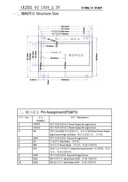
、结构尺寸StructureSize 一5V 供电5V IO 电平二、接口定义Pin Assignment(P2&P3)序号(No.)定义(SYMBOL )说明(Description )1VCC3.3数字电路电源电压Power Supply for Logic Circuit 2VCC3.3数字电路电源电压Power Supply for Logic Circuit 3EN 模块13v OLED 供电使能信号,高有效OLE Panel Power Enable Signal active High to Enable ,默认内部弱上拉,可不接。
4GND 数字电路电源地Ground of Logic Circuit 5CS 片选信号Chip Select 低有效,6RES 复位信号Power Reset 低有效,需IO 引脚控制7D/C 数据与命令控制信号Data/Command Control 高为数据,低为命令。
需IO 引脚控制8GND 数字电路电源地Ground of Logic Circuit 9SCLK SPI 时钟信号Serial Clock of SPI 。
需IO 引脚控制10SDIN SPI 输入信号Serial Data of SPI 。
需IO 引脚控制OLED2.4寸1309_3.3V一、产品介绍General SpecificationsDiagonal Size尺寸 2.4”Color颜色Yellow、Green、Blue、WhiteType类型MonochromePixel Number分辨率128x64Module Size(mm)模组尺寸62.1×53.3×9Active Size(mm)显示区域55.01×27.49Driver IC驱动IC SSD1309Interface接口4_Wire SPISupply Voltage供电电压 3.3VVoltage Range建议电压范围 1.65V~3.3VMax Voltage最大极限电压4VMin Voltage最小极限电压 1.65VView Angle视角>160degree全视角Contrast对比度>10000:1Brightness(cd/m2)亮度(绿色)120(Typ)@13V(20000Hours)Power功耗由点亮的像素决定30%像素点亮<260mw50%像素点亮<345mw100%像素点亮(实际使用中用不到)<515mwBrightness(cd/m2)(黄色)80(Typ)@13V(15000Hours)Power功耗由点亮的像素决定30%像素点亮<260mw50%像素点亮<380mw100%像素点亮(实际使用中用不到)<590mwBrightness(cd/m2)(白色)80(Typ)@13V(30000Hours)Power功耗由点亮的像素决定30%像素点亮<300mw50%像素点亮<440mw100%像素点亮(实际使用中用不到)<690mwBrightness(cd/m2)(蓝色)80(Typ)@13V(15000Hours)Power功耗由点亮的像素决定30%像素点亮<325mw50%像素点亮<470mw100%像素点亮(实际使用中用不到)<720mwWeight(g)重量8.6Assembly连接方式10Pin1.0mm FPC Connector and2.54mm Metal pins四、SPI接口特性SPI Timing Characteristics。
BE460GFD一B31液晶屏规格书

BE460GFD一B31液晶屏规格书
1、段码屏的走线图:顾名思义,为整个屏幕的走线逻辑,哪些走线控制哪些引脚,哪些引脚控制哪些笔段,在不懂的人看来都是些奇怪的线条,一般需要公司的设计人员才能看得懂。
2、段码屏的真值表:真值表是用来给技术开发控制系统程序的时候使用的代码,当拿到图纸后一定要好好核对这项内容,仔细检测连接的笔段有没有问题,如如果有问题的话需要及时反馈给液晶屏厂家
3、液晶屏的显示效果图:指的是在段码液晶屏上的所有图案全部显示的一个效果图,这个图的主要作用是为了检查图案的正确性,以及颜色,图案的美观性等;
4、液晶屏的尺寸参数图:其中包含液晶屏的外形尺寸,显示尺寸,针脚尺寸和间距,屏幕材质,偏光片类型,显示模式,温度区间,观察角度,连接方式,驱动条件等。
以上就是规格书图纸的全部内容了。
所以,在定制液晶屏的时候第一时间需要把这些内容对接好,自身的产品上应用的一些参数,告诉给段码屏的生产厂家,让他们帮你出好图纸确认好,然后才是是生产环节。
苏州扬润电子有限公司,是一家专注段码屏(LCD)、液晶显示模块(LCM)、背光源(LED)的生产厂家。
产品广泛运用于仪器仪表,小家电控制板,电能表,温奶器显示屏,遥控器显示屏,医疗保健器械以及各种小家电等产品。
9.7英寸液晶屏规格书XHS100IPS242-A(9.7寸)

SHENZHEN XINHANGSHENG CO,LTD.,Product Type :Model NO.: Ve r s i on :Please sign the cover page of the spec for your approval and return it to our local sales within a month after your receipt of the spec from SHENZHEN XINHANGSHENG TECHNOLOGY CO.,LTD . In the case does not receive the signed spec even after one month later, in general we will consider that the spec was already accepted by your company.PreparedCheckedApprovedDateTECHNOLOGY SHENZHEN XINHANGSHENG TECHNOLOGY CO.,LTD . SPECIFICATIONXHS100IPS242-A*4)If users use the product out off the environmemtal operation range (temperature and humidity ), it will have visual quality concerns.【Note2】Please adjust VCOM to make the flicker level be minimum.256 gray pattern Black Pattern0<T1≦10ms T2>0ms T3>20ms T4>0ms T5>10ms 0<T6≦10ms T7>0msT8>0ms T9>0ms T10>0ms 0<T6≦10ms 0<T11≦10ms T12≧200ms T13≧200ms*2) A :Anode(+),K :Cathode(-)*3) Suggestion: Using the constant current control to avoid the leakage light and brightness quality issue. *4) Definition of Led lifetime :Luminance < Initial luminance 50%.4. INTERFACE CONNECTIONv.0.1【Note1】UPDN and SHLR control functionRight5. INPUT SIGNAL(DE ONLY MODE) 5.1 Timing Specification5.2 Timing Waveforms5.3 Output Timing5.4 Color Data ReferenceNote :1) Gray level:Color(n):n is level order; higher n means brighter level.2) DATA:1: high,0: low7. OPTICAL CHARACTERISTICS【Note2】Definition of contrast ratio :Contrast Ratio (CR)= (White) Luminance of ON ÷ (Black) Luminance of OFF【Note3】Definition of luminance:Measure white luminance on the point 5 as figure.7-1Definition of Luminance Uniformity: Measure white luminance on the point1~9 as figure.7-1 △L = [L(MIN)/L(MAX)]×100Fig.7-1 Measuring point【Note4】Definition of Viewing Angle(θ,ψ),refer to Fig.7-2 as below:【Note5】Definition of Response Time.(White-Black)Image Sticking pattern8.3 Electrostatic DischargeTEST ITEM CONDITIONS Note150pF,330,±8kV&±15kV air& contact test 1 ESD200pF,0,±200V contact test 2 【Note】 Measure1: LCD glass and metal bezel2: IF connector pinsTBD。
OLED2.4寸显示屏 液晶屏 规格书

、结构尺寸StructureSize 一5V 供电5V IO 电平二、接口定义Pin Assignment(P2&P3)序号(No.)定义(SYMBOL )说明(Description )1VCC3.3数字电路电源电压Power Supply for Logic Circuit 2VCC3.3数字电路电源电压Power Supply for Logic Circuit 3EN 模块13v OLED 供电使能信号,高有效OLE Panel Power Enable Signal active High to Enable ,默认内部弱上拉,可不接。
4GND 数字电路电源地Ground of Logic Circuit 5CS 片选信号Chip Select 低有效,6RES 复位信号Power Reset 低有效,需IO 引脚控制7D/C 数据与命令控制信号Data/Command Control 高为数据,低为命令。
需IO 引脚控制8GND 数字电路电源地Ground of Logic Circuit 9SCLK SPI 时钟信号Serial Clock of SPI 。
需IO 引脚控制10SDIN SPI 输入信号Serial Data of SPI 。
需IO 引脚控制OLED2.4寸1309_3.3V一、产品介绍General SpecificationsDiagonal Size尺寸 2.4”Color颜色Yellow、Green、Blue、WhiteType类型MonochromePixel Number分辨率128x64Module Size(mm)模组尺寸62.1×53.3×9Active Size(mm)显示区域55.01×27.49Driver IC驱动IC SSD1309Interface接口4_Wire SPISupply Voltage供电电压 3.3VVoltage Range建议电压范围 1.65V~3.3VMax Voltage最大极限电压4VMin Voltage最小极限电压 1.65VView Angle视角>160degree全视角Contrast对比度>10000:1Brightness(cd/m2)亮度(绿色)120(Typ)@13V(20000Hours)Power功耗由点亮的像素决定30%像素点亮<260mw50%像素点亮<345mw100%像素点亮(实际使用中用不到)<515mwBrightness(cd/m2)(黄色)80(Typ)@13V(15000Hours)Power功耗由点亮的像素决定30%像素点亮<260mw50%像素点亮<380mw100%像素点亮(实际使用中用不到)<590mwBrightness(cd/m2)(白色)80(Typ)@13V(30000Hours)Power功耗由点亮的像素决定30%像素点亮<300mw50%像素点亮<440mw100%像素点亮(实际使用中用不到)<690mwBrightness(cd/m2)(蓝色)80(Typ)@13V(15000Hours)Power功耗由点亮的像素决定30%像素点亮<325mw50%像素点亮<470mw100%像素点亮(实际使用中用不到)<720mwWeight(g)重量8.6Assembly连接方式10Pin1.0mm FPC Connector and2.54mm Metal pins四、SPI接口特性SPI Timing Characteristics。
32寸液晶电视规格书

32寸液晶电视规格书
规格参数:
产品类别:32寸液晶三合一电视机(电视+显示器+AV)
最高分辨率:1920*1080的显示分辨率,感受丝绸般细腻的视觉享受
亮度:500cd/㎡
对比度:500:1
点距:0.297
显示颜色:16.7m
水平扫描频率(KHz):30~60
垂直扫描频率(Hz):50~75
视角:160(H),140(V)
音箱:5W+5W
输入端口:电源、VGA、AV、TV、HDMI、音频输入、音频输出 USB(可选)响应时间:4ms
菜单语言:English Chinese German Spanish Italian French
按键方式:Auto Menu Power Left Right输入电源:DC +1V 4A支持立式/壁挂
- 1、下载文档前请自行甄别文档内容的完整性,平台不提供额外的编辑、内容补充、找答案等附加服务。
- 2、"仅部分预览"的文档,不可在线预览部分如存在完整性等问题,可反馈申请退款(可完整预览的文档不适用该条件!)。
- 3、如文档侵犯您的权益,请联系客服反馈,我们会尽快为您处理(人工客服工作时间:9:00-18:30)。
Specification 930.24(H) x 523.26 (V) (42.02” diagonal)
938.3 (H) x 531.3 (V) a-si TFT active matrix 1920x R.G.B. x 1080 0.1615 (H) x 0.4845 (V)
Approval
1. GENERAL DESCRIPTION 1.1 OVERVIEW
V420H1- L01 is a 42” TFT Liquid Crystal Display module with 24-CCFL Backlight unit and 2ch-LVDS interface. This module supports 1920 x 1080 HDTV format and can display true 16.7M colors (8-bit/color). The inverter module for backlight is built-in.
3.2 BACKLIGHT UNIT
3.2.1 CCFL(Cold Cathode Fluorescent Lamp) CHARACTERISTICS
3.2.2 INVERTER CHARACTERISTICS
3.2.3 INVERTER INTERTFACE CHARACTERISTICS
4. BLOCK DIAGRAM 4.1 TFT LCD MODULE
Page (New)
Section
Description
All
All Approval Specification wued Date: Sept.30.05 Model No.: V420H1-L01
Approval
3
The information described in this technical specification is tentative and it is possible to be changed without prior
-------------------------------------------------------
5
3. ELECTRICAL CHARACTERISTICS
-------------------------------------------------------
7
3.1 TFT LCD MODULE
-------------------------------------------------------
25
8. PRECAUTIONS 8.1 ASSEMBLY AND HANDLING PRECAUTIONS 8.2 SAFETY PRECAUTIONS
-------------------------------------------------------
-------------------------------------------------------
31
11. MECHANICAL CHARACTERISTICS
-------------------------------------------------------
33
2
The information described in this technical specification is tentative and it is possible to be changed without prior
29
9. DEFINITION OF LABELS 9.1 CMO MODULE LABEL
-------------------------------------------------------
30
10. PACKAGEING 10.1 PACKING SPECIFICATION 10.2 PACKING METHOD
-------------------------------------------------------
4
2. ABSOLUTE MAXIMUM RATINGS 2.1 ABSOLUTE RATINGS OF ENVIRONMENT 2.2 ELECTRICAL ABSOLUTE RATINGS 2.2.1 TFT LCD MODULE 2.2.2 BACKLIGHT UNIT
notice. Please contact CMO ’s representative while your product design is based on this specification. Version2.0
Issued Date: Sept.30.05 Model No.: V420H1-L01
6. INTERFACE TIMING 6.1 INPUT SIGNAL TIMING SPECIFICATIONS 6.2 POWER ON/OFF SEQUENCE
-------------------------------------------------------
22
7. OPTICAL CHARACTERISTICS 7.1 TEST CONDITIONS 7.2 OPTICAL SPECIFICATIONS
1.2 FEATURES
- Ultra wide viewing angle – Super MVA technology - High brightness (550 nits) - High contrast ratio (1000:1) - Fast response time (8 ms) - High color saturation (NTSC 75%) - Full HD (1920 x 1080 pixels) resolution - DE (Data Enable) only mode - LVDS (Low Voltage Differential Signaling) interface - 180 degree rotation display option - Optimized response time for 50 / 60 Hz frame rate
14
5.1 TFT LCD MODULE LVDS input
5.2 TFT LCD MODULE Power input
5.3 BACKLIGHT UNIT
5.4 INVERTER UNIT
5.5 BLOCK DIAGRAM OF INTERFACE
5.6 LVDS INTERFACE
5.7 COLOR DATA INPUT ASSIGNMENT
notice. Please contact CMO ’s representative while your product design is based on this specification. Version2.0
Issued Date: Sept.30.05 Model No.: V420H1-L01
577 44.8 53
mm
Note (1)
mm
mm
-
Weight
11000
11200
11400
g
-
Note (1) Please refer to the attached drawings for more information of front and back outline dimensions.
Approval
1.5 MECHANICAL SPECIFICATIONS
Item
Min.
Typ.
Max.
Unit
Note
Horizontal(H)
982.3
983
984
mm
Module Size
Vertical(V)
Depth(D)
W/PCB-Cover W/I INV
575.3 43.1 51
576 43.8 52
(1)
-
-
Note (1) Please refer to the attached drawings in chapter 9 for more information about the front and
back outlines.
4
The information described in this technical specification is tentative and it is possible to be changed without prior
Issued Date: Sept.30.05 Model No.: V420H1-L01
Approval
TFT LCD Approval Specification
MODEL NO.: V420H1 - L01
Costumer:___________________________________ Approval by:_________________________________ Note:
Issued Date: Sept.30.05 Model No.: V420H1-L01
Approval
- CONTENTS -
REVISION HISTORY
-------------------------------------------------------
3
1. GENERAL DESCRIPTION 1.1 OVERVIEW 1.2 FEATURES 1.3 APPLICATION 1.4 GENERAL SPECIFICATIONS 1.5 MECHANICAL SPECIFICATIONS