74LVC245(电压逻辑隔离)
74LVCH162245A(总线隔离,U20 U21 U22)

查询74LVC162245A供应商SSOP48:plastic shrink small outline package; 48 leads; body width 7.5 mm SOT370-1TSSOP48:plastic thin shrink small outline package; 48 leads; body width 6.1mm SOT362-1NOTESDefinitionsShort-form specification — The data in a short-form specification is extracted from a full data sheet with the same type number and title. For detailed information see the relevant data sheet or data handbook.Limiting values definition — Limiting values given are in accordance with the Absolute Maximum Rating System (IEC 134). Stress above one or more of the limiting values may cause permanent damage to the device. These are stress ratings only and operation of the device at these or at any other conditions above those given in the Characteristics sections of the specification is not implied. Exposure to limiting values for extended periods may affect device reliability.Application information — Applications that are described herein for any of these products are for illustrative purposes only. Philips Semiconductors make no representation or warranty that such applications will be suitable for the specified use without further testing or modification.DisclaimersLife support — These products are not designed for use in life support appliances, devices or systems where malfunction of these products can reasonably be expected to result in personal injury. Philips Semiconductors customers using or selling these products for use in such applications do so at their own risk and agree to fully indemnify Philips Semiconductors for any damages resulting from such application.Right to make changes — Philips Semiconductors reserves the right to make changes, without notice, in the products, including circuits, standard cells, and/or software, described or contained herein in order to improve design and/or performance. Philips Semiconductors assumes no responsibility or liability for the use of any of these products, conveys no license or title under any patent, copyright, or mask work right to these products, and makes no representations or warranties that these products are free from patent, copyright, or mask work right infringement, unless otherwise specified.Philips Semiconductors811 East Arques AvenueP.O. Box 3409Sunnyvale, California 94088–3409Telephone 800-234-7381© Copyright Philips Electronics North America Corporation 1998All rights reserved. Printed in U.S.A.print code Date of release: 05-96。
74HC245简介

74HC04 的作用:6位反相器。
第七脚GND,电源地。
第14脚步VCC,电源正极信号由A端输入Y端反相输出,A1与Y1为一组,其它类推。
例:A1=“1”则Y1=“0” ﹑A1=“0”则Y1=“1”,其它组功能一样。
74HC138的作用:八位二进制译十进制译码器。
第8脚GND,电源地。
第15脚VCG,电源正极、第1~3脚A﹑B﹑C﹑二进制输入脚。
第4~6脚片选信号控制,只有在4﹑5脚为“0”6脚为“1”时,才会被选通,输出受A﹑B﹑C﹑信号控制。
其它任何组合方式将不被选通,且Y0~Y7输出全为“1”。
通过控制选通脚来级联,使之扩展到十六位。
例:G2A=0,G2B=0,G1=1,A=1,B=0,C=0,则YO为“0”Y1~Y7为“1”,74HC595的作用:LED驱动芯片,8位移位锁存器。
第8脚GND,电源地。
第16脚VCC,电源正极第14脚DATA,串行数据输入口,显示数据由此进入,必须有时钟信号的配合才能移入。
第13脚EN,使能口,当该引脚上为“1”时QA~QH口全部为“1”,为“0”时QA~QH 的输出由输入的数据控制。
第12脚STB,锁存口,当输入的数据在传入寄存器后,只有供给一个锁存信号才能将移入的数据送QA~QH口输出。
第11脚CLK,时钟口,每一个时钟信号将移入一位数据到寄存器。
第10脚SCLR,复位口,只要有复位信号,寄存器内移入的数据将清空,显示屏不用该脚,一般接VCC。
第9脚DOUT,串行数据输出端,将数据传到下一个第15﹑1~7脚,并行输出口也就是驱动输出口,驱动LED。
4953的作用:行驱动管,功率管。
其内部是两个CMOS管,1﹑3脚VCC,2﹑4脚控制脚,2脚控制7﹑8脚的输出4脚控 5﹑6脚的输出,只有当2﹑4脚为“0”时,7﹑8﹑5﹑6才会输出,否则输出为高阻状态。
TB62726的作用:LED驱动芯片,16位移位锁存器。
第1脚GND,电源地。
第24脚VCC,电源正极第2脚DATA,串行数据输入第3脚CLK,时钟输入第4脚STB,锁存输入第23脚输出电流调整端,接电阻调整第22脚DOUT,串行数据输入第21脚EN,使能输入其它功能与74HC595相似,只是TB62726是16位移位锁存器,并带输出电流调整功能,但在并行输出口上不会出现高电平,只有高阻状态和低电平状态。
74lvc245中文说明
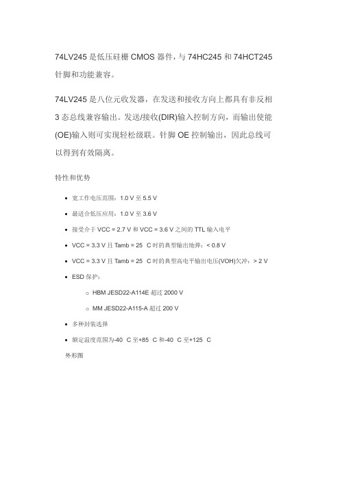
74LV245是低压硅栅CMOS器件,与74HC245和74HCT245针脚和功能兼容。
74LV245是八位元收发器,在发送和接收方向上都具有非反相3态总线兼容输出。
发送/接收(DIR)输入控制方向,而输出使能(OE)输入则可实现轻松级联。
针脚OE控制输出,因此总线可以得到有效隔离。
特性和优势
•宽工作电压范围:1.0 V至5.5 V
•最适合低压应用:1.0 V至3.6 V
•接受介于VCC = 2.7 V和VCC = 3.6 V之间的TTL输入电平
•VCC = 3.3 V且T amb = 25 °C时的典型输出地弹:< 0.8 V
•VCC = 3.3 V且T amb = 25 °C时的典型高电平输出电压(VOH)欠冲:> 2 V •ESD保护:
o HBM JESD22-A114E超过2000 V
o MM JESD22-A115-A超过200 V
•多种封装选择
•额定温度范围为-40 °C至+85 °C和-40 °C至+125 °C
外形图
显示功能框图
真值表
INPUTS INPUTS/OUTPUT OE DIR An Bn
H=高电压L=低电压X=无输入、Z=高阻态。
74HC245中文资料_数据手册_参数

74HC245八路巴士TRANCEIVER;三态 14.修订历史表13:修订记录文档ID发布日期数据表状态更改注意文档.数取代版本 74HC_HCT245_3 20050131产品数据表 - 9397 750 14502 74HC_HCT245_CNV_2莫迪科幻阳离子: ? 本数据表的格式经过重新设计以符 合新的演示文稿和飞利浦半导体的信息标准 ?第4节“订购信息”,第6节“固定信息”和第13节“包装大纲“修改为包含DHVQFN20 包. 74HC_HCT245_CNV_2 19930930产品SPECI FI CATION 9397 750 14502 ? 74HC245 NV 2005.保留所有权利. 74HC245产品数据表 2005年1月3日至31日 13的22飞利浦半导体 74HC245; 74HCT245八 路巴士TRANCEIVER;三态 12.波形测量点在表11中给出. V OL 和V OH 是输出负载时发生的典型电压输出下降.图5.输入(AN,BN) 输出(BN,AN)传播延迟和输出转换时间测量点在表11中给出. V OL 和V OH 是输出负载时发生的典型电压输出下降.图6. 3态输出 启用和禁用时间表11:测量点类型输入产量 74HC245保留所有权利.产品数据表 2005年1月3日至3月31日 13的22飞利浦半导体 74HC245; 74HCT245八路公交车三态波形测量点在表 11中给出. V OL 和V OH 是输出负载时发生的典型电压输出降.图5.输入(An,Bn)输出(Bn,An)传播延迟和输出转换时间测量点 在表11中给出. V OL 和V OH 是输出负载时发生的典型电压输出降.图6. 3状态输出使能和禁止时间表11:测量点类型输入产量 V M V M 74HC245 0.5V CC 0.5V CC 74HCT245 1.3 V 1.3 V 001aac433 t PLH t PHL VM V M 90% 10% V M V M Bn,输出 An,Bn输入 V 我 GND V OH V OL t TLH t THL 001aac479 t PLZ t PHZ输出残输出启用 90% 10%输出启用 OE输入 V 我 V CC V OL V OH GND GND V M t PZL t PZH V M V M产量 LOW-到关关到LOW产量 74HC245输出频率; C L = pF中的输出负载电容; V CC =电源电压V; N =输入切换次数; Σ(C L ×V CC 2 ×f o )=输出和.表10:动态特 性类型74HCT245 GND = 0 V;测试电路见图7.符号参数条件敏典型马克斯单元 T amb = 25°C t PHL ,t PLH传播延迟A到Bn或Bn到安见 图5 V CC = 4.5 V - 12 22 NS V CC = 5.0 V; C L = 15pF - 10 - NS t PZH ,t PZL 3状态输出使能时间OE A或OE到Bn V CC = 4.5V; 见图6 1630ns PHZ ,t PLZ 3状态输出禁用时间OE A或OE到Bn V CC = 4.5V; 见图6 - 1630ns t THL ,t TLH输出转换时间 V CC = 4.5V; 见图5 - 五 12 NS C PD功耗电容每个收发器 V I = GND至V CC - 1.5 V [1] -30 - pF的 T amb = -40°C至+85°C t PHL ,t PLH传播延迟A到Bn或Bn到 安 V CC = 4.5V; 见图5 --28 NS t PZH ,t PZL 3状态输出使能时间OE A或OE到Bn V CC = 4.5V; 见图6 --38 NS PHZ ,t PLZ 3状态输出禁 用时间OE A或OE到Bn V CC = 4.5V; 见图6 --38 NS t THL ,t TLH输出转换时间 V CC = 4.5V; 见图5 --15 NS T amb = -40°C至+125°C t PHL ,t PLH传播延迟A到Bn或Bn到安 V CC = 4.5V; 见图5 --33 NS t PZH ,t PZL 3状态输出使能时间
SN74LVC245资料
元器件交易网IMPORTANT NOTICETexas Instruments and its subsidiaries (TI) reserve the right to make changes to their products or to discontinueany product or service without notice, and advise customers to obtain the latest version of relevant informationto verify, before placing orders, that information being relied on is current and complete. All products are soldsubject to the terms and conditions of sale supplied at the time of order acknowledgement, including thosepertaining to warranty, patent infringement, and limitation of liability.TI warrants performance of its semiconductor products to the specifications applicable at the time of sale inaccordance with TI’s standard warranty. Testing and other quality control techniques are utilized to the extentTI deems necessary to support this warranty. Specific testing of all parameters of each device is not necessarilyperformed, except those mandated by government requirements.CERTAIN APPLICATIONS USING SEMICONDUCTOR PRODUCTS MAY INVOLVE POTENTIAL RISKS OFDEATH, PERSONAL INJURY, OR SEVERE PROPERTY OR ENVIRONMENTAL DAMAGE (“CRITICALAPPLICATIONS”). TI SEMICONDUCTOR PRODUCTS ARE NOT DESIGNED, AUTHORIZED, ORWARRANTED TO BE SUITABLE FOR USE IN LIFE-SUPPORT DEVICES OR SYSTEMS OR OTHERCRITICAL APPLICATIONS. INCLUSION OF TI PRODUCTS IN SUCH APPLICATIONS IS UNDERSTOOD TOBE FULLY AT THE CUSTOMER’S RISK.In order to minimize risks associated with the customer’s applications, adequate design and operatingsafeguards must be provided by the customer to minimize inherent or procedural hazards.TI assumes no liability for applications assistance or customer product design. TI does not warrant or representthat any license, either express or implied, is granted under any patent right, copyright, mask work right, or otherintellectual property right of TI covering or relating to any combination, machine, or process in which suchsemiconductor products or services might be or are used. TI’s publication of information regarding any thirdparty’s products or services does not constitute TI’s approval, warranty or endorsement thereof.Copyright © 1998, Texas Instruments Incorporated。
74LVC245A_04中文资料

1/12July 2004s 5V TOLERANT INPUTSs HIGH SPEED: t PD = 6.3ns (MAX.) at V CC = 3V sPOWER DOWN PROTECTION ON INPUTS AND OUTPUTSsSYMMETRICAL OUTPUT IMPEDANCE:|I OH | = I OL = 24mA (MIN) at V CC = 3Vs PCI BUS LEVELS GUARANTEED AT 24 mA sBALANCED PROPAGATION DELAYS:t PLH ≅ t PHLsOPERATING VOLTAGE RANGE:V CC (OPR) = 1.65V to 3.6V (1.2V Data Retention)sPIN AND FUNCTION COMPATIBLE WITH 74 SERIES 245sLATCH-UP PERFORMANCE EXCEEDS 500mA (JESD 17)sESD PERFORMANCE:HBM > 2000V (MIL STD 883 method 3015); MM > 200VDESCRIPTIONThe 74LVC245A is a low voltage CMOS OCTAL BUS TRANSCEIVER (3-STATE) fabricated with sub-micron silicon gate and double-layer metal wiring C 2MOS technology. It is ideal for 1.65 to 3.6V CC operations and low power and low noise applications.This IC is intended for two-way asynchronous communication between data buses and the direction of data transmission is determined by DIR input. The enable input G can be used to disable the device so that the buses are effectively isolated.It has more speed performance at 3.3V than 5V AC/ACT family, combined with a lower power consumption.All inputs are equipped with protection circuits against static discharge, giving them 2KV ESD immunity and transient excess voltage.All floating bus terminals during High Z State must be held HIGH or LOW.74LVC245ALOW VOLTAGE CMOS OCTAL BUS TRANSCEIVER(NOT INVERTED) HIGH PERFORMANCE.Table 1: Order CodesPACKAGE T & R SOP 74LVC245AMTR TSSOP74LVC245ATTR74LVC245A2/12Figure 2: Input And Output Equivalent CircuitTable 2: Pin DescriptionTable 3: Truth TableX : Don’t CareZ : High ImpedanceTable 4: Absolute Maximum RatingsAbsolute Maximum Ratings are those values beyond which damage to the device may occur. Functional operation under these conditions is not implied1) I O absolute maximum rating must be observed 2) V O< GNDPIN N°SYMBOL NAME AND FUNCTION 1DIR Directional Control 2, 3, 4, 5, 6, 7, 8, 9A1 to A8Data Inputs/Outputs 18, 17, 16, 15, 14, 13, 12, 11B1 to B8Data Inputs/Outputs19GOutput Enable Input 10GND Ground (0V)20V CCPositive Supply VoltageINPUTS FUNCTION OUTPUT G DIR A BUSB BUSYn L L OUTPUT INPUT A = B L H INPUT OUTPUT B = A HXZ ZZSymbol ParameterValue Unit V CC Supply Voltage -0.5 to +7.0V V I DC Input Voltage-0.5 to +7.0V V O DC Output Voltage (High Impedance or V CC = 0V)-0.5 to +7.0V V O DC Output Voltage (High or Low State) (note 1)-0.5 to V CC + 0.5V I IK DC Input Diode Current- 50mA I OK DC Output Diode Current (note 2)- 50mA I O DC Output Current ± 50mA I CC or I GND DC V CC or Ground Current per Supply Pin± 100mA T stg Storage Temperature -65 to +150°C T LLead Temperature (10 sec)300°C74LVC245A3/12Table 5: Recommended Operating Conditions1) Truth Table guaranteed: 1.2V to 3.6V 2) V IN from 0.8V to 2V at V CC = 3.0VTable 6: DC SpecificationsSymbol ParameterValue Unit V CC Supply Voltage (note 1) 1.65 to 3.6V V I Input Voltage0 to 5.5V V O Output Voltage (High Impedance or V CC = 0V)0 to 5.5V V O Output Voltage (High or Low State)0 to V CC V I OH , I OL High or Low Level Output Current (V CC = 3.0 to 3.6V)± 24mA I OH , I OL High or Low Level Output Current (V CC = 2.7 to 3.0V)± 12mA I OH , I OL High or Low Level Output Current (V CC = 2.3 to 2.7V)±8mA I OH , I OL High or Low Level Output Current (V CC = 1.65 to 2.3V)±4mA T op Operating Temperature-55 to 125°C dt/dvInput Rise and Fall Time (note 2)0 to 10ns/VSymbolParameterTest ConditionValueUnitV CC (V)-40 to 85 °C -55 to 125 °C Min.Max.Min.Max.V IHHigh Level Input Voltage 1.65 to 1.950.65V CC0.65V CC V2.3 to 2.7 1.7 1.72.7 to3.622V ILLow Level Input Voltage1.65 to 1.950.35V CC0.35V CC V 2.3 to 2.70.70.72.7 to 3.60.80.8V OHHigh Level Output Voltage1.65 to 3.6I O =-100 µA V CC -0.2V CC -0.2V1.65I O =-4 mA 1.2 1.22.3I O =-8 mA 1.7 1.72.7I O =-12 mA 2.2 2.23.0I O =-18 mA 2.4 2.43.0I O =-24 mA 2.22.2V OLLow Level Output Voltage1.65 to 3.6I O =100 µA 0.20.2V 1.65I O =4 mA 0.450.452.3I O =8 mA 0.70.72.7I O =12 mA 0.40.43.0I O =24 mA 0.550.55I I Input Leakage Current 3.6V I = 0 to 5.5V ± 5± 5µA I off Power Off Leakage Current0V I or V O = 5.5V 1010µA I OZHigh Impedance Output Leakage Current3.6V I = V IH orV IL V O = 0 to 5.5V ± 10± 10µA I CCQuiescent Supply Current3.6V I = V CC or GND1010µA V I or V O = 3.6 to5.5V± 10± 10∆I CCI CC incr. per Input2.7 to3.6V IH = V CC -0.6V500500µA74LVC245A4/12Table 7: Dynamic Switching Characteristics1) Number of output defined as "n". Measured with "n-1" outputs switching from HIGH to LOW or LOW to HIGH. The remaining output is measured in the LOW state.Table 8: AC Electrical Characteristics1) Skew is defined as the absolute value of the difference between the actual propagation delay for any two outputs of the same device switch-ing in the same direction, either HIGH or LOW (t OSLH = | t PLHm - t PLHn |, t OSHL = | t PHLm - t PHLn |2) Parameter guaranteed by designTable 9: Capacitive Characteristics1) C PD is defined as the value of the IC’s internal equivalent capacitance which is calculated from the operating current consumption without load. (Refer to Test Circuit). Average operating current can be obtained by the following equation. I CC(opr) = C PD x V CC x f IN + I CC /n (per circuit)SymbolParameterTest ConditionValue UnitV CC (V)T A = 25 °C Min.Typ.Max.V OLP Dynamic Low Level Quiet Output (note 1)3.3C L = 50pFV IL = 0V, V IH = 3.3V0.8V V OLV-0.8SymbolParameterTest ConditionValueUnitV CC (V)C L (pF)R L (Ω)t s = t r (ns)-40 to 85 °C -55 to 125 °C Min.Max.Min.Max.t PLH t PHLPropagation Delay Time1.65 to 1.953010002.0 2.09.0 2.012ns2.3 to 2.730500 2.0 2.08.0 2.010.52.750500 2.5 1.57.3 1.58.83.0 to 3.650500 2.5 1.0 6.3 1.07.6t PZL t PZHOutput Enable Time 1.65 to 1.95301000 2.0 2.012 2.016ns2.3 to 2.730500 2.0 2.09.5 2.012.52.750500 2.5 1.09.0 1.0113.0 to 3.650500 2.5 1.08.5 1.010t PLZ t PHZOutput Disable Time 1.65 to 1.95301000 2.0 2.011 2.014ns2.3 to 2.730500 2.0 2.09.0 2.0122.750500 2.5 2.08.5 2.0103.0 to 3.6505002.52.07.5 2.09.0t OSLH t OSHLOutput To Output Skew Time (note1, 2)2.7 to3.611nsSymbolParameterTest ConditionValue UnitV CC (V)T A = 25 °C Min.Typ.Max.C IN Input Capacitance4pF C PDPower Dissipation Capacitance (note 1)1.8f IN = 10MHz28pF 2.5303.33474LVC245A5/12Figure 3: Test CircuitR T = Z OUT of pulse generator (typically 50Ω)Table 10: Test Circuit And Waveform Symbol ValueFigure 4: Waveform - Propagation Delays (f=1MHz; 50% duty cycle)SymbolV CC1.65 to 1.95V2.3 to 2.7V 2.7V3.0 to 3.6V C L 30pF 30pF 50pF 50pF R L = R 11000Ω500Ω500Ω500ΩV S 2 x V CC 2 x V CC 6V 6V V IH V CC V CC 2.7V 2.7V V M VCC /2V CC /2 1.5V 1.5V V OH V CC V CC 3.0V 3.0V V X V OL + 0.15V V OL + 0.15V V OL + 0.3V V OL + 0.3V VY V OH - 0.15V V OH - 0.15V V OH - 0.3V V OH - 0.3V t r = t r<2.0ns<2.0ns<2.5ns<2.5ns74LVC245AFigure 5: Waveform - Output Enable And Disable Time (f=1MHz; 50% duty cycle)6/1274LVC245A7/12DIM.mm.inch MIN.TYPMAX.MIN.TYP.MAX.A 2.35 2.650.0930.104A10.10.300.0040.012B 0.330.510.0130.020C 0.230.320.0090.013D 12.6013.000.4960.512E 7.47.60.2910.299e 1.270.050H 10.0010.650.3940.419h 0.250.750.0100.030L 0.4 1.270.0160.050k 0°8°0°8°ddd0.1000.004SO-20 MECHANICAL DATA0016022D74LVC245A8/12DIM.mm.inchMIN.TYPMAX.MIN.TYP.MAX.A 1.20.047A10.050.150.0020.0040.006A20.81 1.050.0310.0390.041b 0.190.300.0070.012c 0.090.200.0040.0079D 6.4 6.5 6.60.2520.2560.260E 6.2 6.4 6.60.2440.2520.260E1 4.34.4 4.480.1690.1730.176e 0.65 BSC0.0256 BSCK 0˚8˚0˚8˚L0.450.600.750.0180.0240.030TSSOP20 MECHANICAL DATAcEbA2AE1D1PIN 1 IDENTIFICATIONA1LK e0087225C74LVC245A Tape & Reel SO-20 MECHANICAL DATAmm.inchDIM.MIN.TYP MAX.MIN.TYP.MAX.A33012.992C12.813.20.5040.519D20.20.795N60 2.362T30.4 1.197Ao10.8110.4250.433Bo13.213.40.5200.528Ko 3.1 3.30.1220.130Po 3.9 4.10.1530.161P11.912.10.4680.4769/1274LVC245ATape & Reel TSSOP20 MECHANICAL DATAmm.inch DIM.MIN.TYP MAX.MIN.TYP.MAX.A33012.992 C12.813.20.5040.519 D20.20.795N60 2.362T22.40.882 Ao 6.870.2680.276 Bo 6.97.10.2720.280 Ko 1.7 1.90.0670.075 Po 3.9 4.10.1530.161 P11.912.10.4680.47610/1274LVC245A Table 11: Revision HistoryDate Revision Description of Changes26-Jul-20044Ordering Codes Revision - pag. 1.11/1274LVC245AInformation furnished is believed to be accurate and reliable. However, STMicroelectronics assumes no responsibility for the consequences of use of such information nor for any infringement of patents or other rights of third parties which may result from its use. No license is granted by implication or otherwise under any patent or patent rights of STMicroelectronics. Specifications mentioned in this publication are subject to change without notice. This publication supersedes and replaces all information previously supplied. STMicroelectronics products are not authorized for use as critical components in life support devices or systems without express written approval of STMicroelectronics.The ST logo is a registered trademark of STMicroelectronicsAll other names are the property of their respective owners© 2004 STMicroelectronics - All Rights ReservedSTMicroelectronics group of companiesAustralia - Belgium - Brazil - Canada - China - Czech Republic - Finland - France - Germany - Hong Kong - India - Israel - Italy - Japan - Malaysia - Malta - Morocco - Singapore - Spain - Sweden - Switzerland - United Kingdom - United States of America12/12。
74hc245工作原理
74hc245工作原理让我来跟你唠唠 74HC245 这个小家伙的工作原理!在电子世界里有个叫 74HC245 的小能手。
这玩意儿别看它个头不大,作用可不小呢!74HC245 就像是一个数据传输的小桥梁。
想象一下,有两组数据线,一组在这边,一组在那边,它们之间没办法直接交流,这时候 74HC245 就闪亮登场啦!它有个很重要的功能,就是能增强信号。
比如说,从一端传来的信号有点弱弱的,经过 74HC245 这么一处理,瞬间变得强壮有力,能够顺利地传到另一端去。
而且哦,74HC245 还能控制数据传输的方向。
这就好比是马路上的交通指挥灯,它能告诉数据,你该往这边走还是往那边走。
当使能端(也就是控制它工作的那个小开关)打开的时候,74HC245 就开始干活啦。
如果是双向传输,那数据就能在两个方向上自由穿梭。
比如说,从 A 端传到 B 端,或者从 B 端传到 A 端,全看当时的需求。
要是设置成单向传输呢,那数据就只能乖乖地沿着指定的方向跑啦。
再跟你讲讲它内部的一些小秘密。
74HC245 里面有好多小小的电路元件,它们就像一群勤劳的小蜜蜂,协同工作,让数据传输变得顺畅无比。
当数据进来的时候,这些小元件会迅速地做出反应,对数据进行处理和调整,确保数据的准确性和完整性。
你可别小看这小小的 74HC245 ,在很多电子设备里都能看到它的身影。
比如说电脑主板上、各种控制器里,它都在默默地发挥着自己的作用。
有时候,我们可能感觉不到它的存在,但它却一直在那里努力工作,为整个系统的正常运行贡献着自己的力量。
就像我们生活中的一些人,虽然不那么起眼,但却在背后默默付出,让我们的生活变得更加美好。
怎么样,是不是对 74HC245 这个小家伙有了一些新的认识呢?它虽然不是什么超级英雄,但在电子世界里,也算是个不可或缺的小角色啦!。
74LVC245(电压逻辑隔离)
V
0 to 5.5
V
Operating temperature Ta
–40 to 85
°C
Output current
I OH
–12
mA
–24*2
mA
I OL
12
mA
24*2
mA
Input rise / fall time *1
tr, tf
10
ns/V
Notes: 1. This item guarantees maximum limit when one input switches.
Ratings
Unit
Conditions
Supply voltage
VCC
–0.5 to 6.0
V
Input diode current
I IK
–50
mA
Input voltage
VI
–0.5 to 6.0
V
Output diode current
I OK
–50
mA
50
mA
Input / output voltage
Waveform : Refer to test circuit of switching characteristics.
2. duty cycle ≤ 50%
Conditions Data retention At operation T / R, OE Output "H" or "L" Output "Z" or VCC:OFF
2
HD74LVC245A
Recommended Operating Conditions
74HC245电路
细的参数规格及各厂商型号替换,请以厂商数据手册为准。
生产工艺
TI 公司
ON 公司
工作电压(V)
输入电平兼容
输出电平兼容
74F
F
4.5~5.5
TTL
TTL
Bipolar 5V-Logic
LS
LS
4.75~5.25
TTL
TTL
ALS
4.5~5.5
TTL
TTL
CD4000 系列
MC1400 系列
3.0~18
DFT2,XV5T2
DTT1,DFT2
US
z 工业级温度范围: -40~85℃
07
Buffer OD
DFT2,XV5T2
DTT1,DFT2
US
08
2-Input AND
DFT2,XV5T2
US
14
Inverter-Schmitt
DFT2,XV5T2
DTT1,DFT2
US
数
优点
16
Buffer
DFT2,XV5T2
150
产品参数仅供参考,以厂家数据手册为准。批量价格,欢迎垂询。更多详情:
免费业务电话:800-880-8051 总机:027-8752 6752 传真:027-8752 6551
CMOS
CMOS
HC
HC
2.0~6.0
CMOS
CMOS
AHC
VHC
2.0~5.5
CMOS
CMOS
AHC1G
MC74VHC1G
2.0~6.0
CMOS
CMOS
CMOS 5V-Logic
HCT
HCT
4.5~5.5
LC245A中文资料
GQN OR ZQN PACKAGE (TOP VIEW)
1234
A B C D E
TERMINAL ASSIGNMENTS
1
2
3
4
A
A1
DIR
VCC
OE
B
A3
B2
A2
B1
C
A5
A4
B4
B3
D
A7
B6
A6
B5
E
GND
A8
B8
B7
FUNCTION TABLE
INPUTS
OE DIR
L
L
L
H
H
X
OPERATION
QFN – RGY
Reel of 1000
SN74LVC245ARGYR
SOIC – DW
Tube of 25 Reel of 2000
SN74LVC245ADW SN74LVC245ADWR
SOP – NS
Reel of 2000
SN74LVC245ANSR
SSOP – DB
Reel of 2000
Please be aware that an important notice concerning availability, standard warranty, and use in critical applications of Texas Instruments semiconductor products and disclaimers thereto appears at the end of this data sheet.
DIR 1 A1 2 A2 3 A3 4 A4 5 A5 6 A6 7 A7 8 A8 9 GND 10
- 1、下载文档前请自行甄别文档内容的完整性,平台不提供额外的编辑、内容补充、找答案等附加服务。
- 2、"仅部分预览"的文档,不可在线预览部分如存在完整性等问题,可反馈申请退款(可完整预览的文档不适用该条件!)。
- 3、如文档侵犯您的权益,请联系客服反馈,我们会尽快为您处理(人工客服工作时间:9:00-18:30)。
Waveform : Refer to test circuit of switching characteristics.
2. duty cycle ≤ 50%
Conditions Data retention At operation T / R, OE Output "H" or "L" Output "Z" or VCC:OFF
Note: The absolute maximum ratings are values which must not individually be exceeded, and furthermore, no two of which may be realized at the same time.
4
HD74LVC245A
Switching Characteristics
Ta = –40 to 85°C
Item Propagation delay time
Symbol VCC (V)
t PLH
2.7
t PHL
3.3±0.3
5.0±0.5
Min Typ Max — — 8.0 1.5 — 7.0 — — 5.5
Test Circuit
VCC
VCC
OE Input Pulse Generator Zout = 50 Ω
T/R
See Function Table
S1 A0 B0
Output
500 Ω S2
CL =
450 Ω
50 pF 50 Ω Scope
OPEN *1 See under table GND
Note:
Function Table
Inputs
OE
T/R
L
L
L
H
H
X
H : High level L : Low level X : Immaterial Z : High impedance
Operation B data to A bus A data to B bus Z
HD74LVC245A
Pin Arrangement
tosLH = | tPLHm - tPLHn|, tosHL = | tPHLm - tPHLn|
Unit ns ns ns ns ns ns ns ns ns ns ns ns pF pF
From (Input) To (Output)
A or B
B or A
OE
A or B
OE
A or B
5
HD74LVC245A
Ta = –40 to 85°C
Symbol VCC (V) Min
Max Unit
VIH
2.7 to 3.6 2.0
—
V
4.5 to 5.5 VCC×0.7 —
V
VIL
2.7 to 3.6 —
0.8
V
4.5 to 5.5 —
VCC×0.3 V
VOH
2.7 to 5.5 VCC –0.2 —
V
2.7
4. Waveform – B shows input conditions such that the output is "H" level when enable by the output control.
7
6.50 6.80 Max
20
11
4.40
1
10
0.65
*0.22+–00..0078 0.20 ± 0.06
2.2
—
V
3.0
2.4
—
V
3.0
2.2
—
V
4.5
3.8
—
V
VOL
2.7 to 5.5 —
2.7
—
0.2
V
0.4
V
3.0
—
0.55 V
4.5
—
0.55 V
I IN
0 to 5.5 —
I OZ
2.7 to 5.5 —
±5.0 µA ±5.0 µA
Output leak current
I OFF
Quiescent supply current ICC
+0.03 –0.04
0.07
Hitachi Code JEDEC EIAJ Weight (reference value)
TTP-20DA — — 0.07 g
Cautions
1. Hitachi neither warrants nor grants licenses of any rights of Hitachi’s or any third party’s patent, copyright, trademark, or other intellectual property rights for information contained in this document. Hitachi bears no responsibility for problems that may arise with third party’s rights, including intellectual property rights, in connection with use of the information contained in this document.
GND
1. tr = 2.5 ns, tf = 2.5 ns 2. Input waveform : PRR = 10 MHz, duty cycle 50%
3. Waveform – A shows input conditions such that the output is "L" level when enable by the output control.
∆ I CC
0
—
2.7 to 3.6 —
2.7 to 5.5 —
3.0 to 3.6 —
20
µA
±10 µA
10
µA
500 µA
பைடு நூலகம்
Test Conditions
IOH = –100 µA IOH = –12 mA
IOH = –24 mA
IOL = 100 µA IOL = 12 mA IOL = 24 mA
10 %
tr
90 % Vref
tPLH
Vref
tf
90 % Vref
10 %
tPHL
Vref
VIH GND VOH VOL
6
HD74LVC245A
Waveforms – 2
tf
90 %
OE
Vref
10 %
Waveform - A
Waveform - B
tZL Vref
tZH Vref
tr 90 %
2.7
———
3.3±0.3 — — 1.0
5.0±0.5 — — 1.0
Input capacitance
CIN
2.7
— 3.0 —
Output capacitance
CO
2.7
— 15.0 —
Note: 1. This parameter is characterized but not tested.
HD74LVC245A
Octal Bidirectional Transceivers with 3-state Outputs
ADE-205-111B(Z) 3rd Edition
December 1996
Description
The HD74LVC245A has eight buffers with three state outputs in a 20 pin package. When (T / R) is high, data flows from the A inputs to the B outputs, and when (T / R) is low, data flows from the B inputs to the A outputs. A and B bus are separated by making enable input (OE) high level. Low voltage and high speed operation is suitable at the battery drive product (note type personal computer) and low power consumption extends the life of a battery for long time operation.
Output enable time
t ZH
2.7
— — 9.5
t ZL
3.3±0.3 1.5 — 8.5
5.0±0.5 — — 7.0
Output disable time
t ZH
2.7
— — 8.5
t LZ
3.3±0.3 1.5 — 7.5
5.0±0.5 — — 6.5
Between outut pins skew *1 tOSLH t OSHL
VI/O
–0.5 to VCC +0.5
V
–0.5 to 6.0
V
Output current
IO
±50
mA
VCC, GND current / pin
ICC or IGND
100
mA