AN2867_ST微控制器振荡器电路设计指南
正弦波振荡器的设计 高频电子线路课程设计
正弦波振荡器的设计高频电子线路课程设计
正弦波振荡器是一种能够产生正弦波的振荡器,在电子线路设计中非常重要。
它有着
广泛的应用,如信号源、调制器和解调器等。
本文主要介绍电子工程中一种高频正弦波振
荡器的设计原理。
正弦波振荡器的设计需要考虑的因素很多,其中比较重要的参数有振荡频率、可靠性、污染物、灵敏度和稳定性等。
综合以上几个参数可以构建出一个满足要求的正弦波振荡器。
实现正弦波振荡器的设计,首先需要搭建电路,电路框图如下所示:
(图)
这是一个普通的多级高频正弦波振荡电路。
它包括四个级别,分别是上放大级、下放
大级、延迟级和信号调节级。
由于这个电路有两个放大级,其频率可以调节范围比较大,但最大的频率不能超过2GHz。
像栅极电容器、延迟电阻等元件可用来控制和调节振荡频率。
这些元件不仅可提升振荡频率,而且还可以降低振荡振幅,以及改善振荡器的可靠
性和稳定性。
正弦波振荡器的设计是一项有趣的研究课题。
它可以满足工业和商业应用的各种需求,正弦波的清晰度和稳定度也极大地增强了电子设备的可靠性。
高频正弦波振荡器的设计原
理完全可以参考上文的框图,依据电路的架构结合参数,可以根据不同的特性需求进行振
荡电路的搭建。
具体实施方法还需要实验进行最后的优化,以获得更好的设计效果。
AN2867ST微控制器振荡器电路设计指南
AN2867Application noteOscillator design guide for ST microcontrollers简介:大局部设计人员对振荡器〔Pierce-Gate topology 皮尔斯门构造〕都很生疏,但真的明白它是如何工作的人并不多,更甭提设计一个适宜的振荡器了。
实际上,很多设计人员并未真正关注过振荡器的设计,直到他们觉察振荡器不正常运行了〔通常这时产品已经投产了〕。
这本是不应当发生的。
很多系统、工程工程的拖延就仅仅是由于一个振荡器没有工作在估量的状态上。
振荡器应当在产品设计阶段就得到足够的重视,并且最好是在投产之前。
这样设计人员才可能避开大批产品被退回来返修那噩梦样的场景。
本应用笔记将介绍皮尔斯〔Pierce〕振荡器的根本原理,并为如何设计一个优良的振荡器供给指导。
同时也会说明如何选取不同的外围元件,并就怎样为振荡器设计一个优良的PCB 供给指导。
本文档的最终局部就如何选取适宜的晶体和外围元件供给一个简洁的指导,并列出一些为STM32 和STM8A/S 推举的晶体型号〔HSE 和LSE〕,以便利快速开头一个设计。
1.石英晶体的特性和模型〔Quartz crystal propertiesandmod e l〕石英晶体是一种压电器件,它能够实现电能和机械能的相互转换。
这个转换发生在谐振频率处。
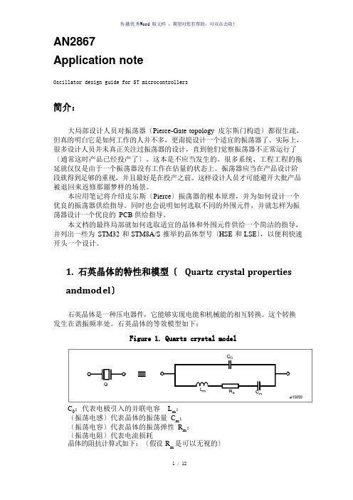
石英晶体的等效模型如下:Figure 1. Quartz crystal modelC 0:代表电极引入的并联电容Lm:〔振荡电感〕代表晶体的振荡量Cm :〔振荡电容〕代表晶体的振荡弹性Rm :〔振荡电阻〕代表电流损耗晶体的阻抗计算式如下:〔假设Rm是可以无视的〕1 / 12图 2 是晶体在频域内的阻抗曲线。
Figure 2.Impedance representation in the frequency domainF s 是晶体在 Z=0 时的串联谐振频率。
它的表达式可以从等式〔1〕中推导出来:F a 是反谐振频率,此时的Z 趋于无穷大。
YXDSP-F28069官方用户手册V1.0(CCS4.20)

� �
浮点单元,具有本地单精度浮点运行功能 可编程控制律加速器(CLA) 32 位浮点数学加速器 代码执行不依赖于主 CPU
�
Viterbi, 复杂数学, 循环校验单元(VCU) 对 C28x ™ 指 令 集 进 行 了 扩展 以 支 持复 数 乘 法、 Viterbi 运 算 及循 环 冗 余校 验 (CRC)
2
Copyright 2009 © YanXu . All rights recerved
南京研旭电气科技有限公司
1
�
芯片特点
高效率 32 位浮点 CPU(TMS320C28x ™ ) 主频 90MHz(11.11ns 周期时间) 16 x 16 和 32 x 32 MAC 运算 16 x 16 双通道 MAC 哈佛(Harvard) 总线架构 连动运算 快速中断响应及处理 统一内存编程模型 高编码效率(采用 C / C++语言和汇编语言)
4
Copyright 2009 © YanXu . All rights recerved
南京研旭电气科技有限公司
2
28069 开发板外设
� ePWM 通过 HC245 外接出 16 路(其中 8 路可复用为 HRPWM) � 通过 74CBTD3384 引出全部 4 路高精度 CAP、2 组 QEP 和 3 路增强型 CAP(eCAP) � 两个 SCI 模块, SCIA 接到了一片 MAX485 上用于 RS485 通信,SCIB 接到了一片 MAX3232 上用于 RS232 通信 � 一个 CAN 模块通过 VP230 芯片引出便于 CAN 组网通信 � I2C 接到了一片 EEPROM 上 � SPIB 接到了 SD 卡上 � AD 部分的外部参考高电压 VREFH 可以通过跳帽 JUMP1 选择(板上有一个 2.5V 参 考电压和 3.3V 参考电压),外部参考低电压 VREFL 通过一个 0Ω电阻接地,所有 AD 输入端口都接了一个 3V 的稳压管防止输入电压过大损坏 AD 模块,如果用户 不需要 3V 稳压管可以自己卸下 � 通过 JP1、JP2、JP3、JP4 引出了所有的 28069 功能管脚 (一些地引脚直接接地 未引出),方便用户二次使用
微芯片技术1996年BASIC PIC16 17振荡器设计说明书
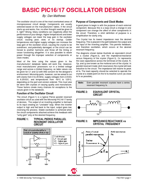
1996 Microchip Technology Inc.FACT001-page 1®BASIC PIC16/17 OSCILLATOR DESIGNBy:Dan MatthewsThe oscillator circuit is one of the most overlooked areas of microprocessor circuit design. Components are usually selected based on the manufacturers' tables. If the circuit starts up and works, fine, no other thought need be given to it, right? Wrong. Many conditions can negatively affect the performance of your design. Higher temperatures and lower supply voltages can lower the loop gain in the oscillator circuit, causing poor, slow, or no startup. Colder temperatures and higher supply voltages can increase the loop gain of the oscillator circuit, causing the crystal to be overdriven, and potentially damaged; or the circuit can be forced to another harmonic and throw off the timing or cease functioning altogether. It is also possible to waste power through the improper selection of components or clock modes.Most of the time using the values given in the manufacturers' databook tables will work fine. However,most manufacturers' processors run in a limited voltage range and across a limited frequency, so table values can be given for C1 and C2 with little concern for the designer's environment. Microchip parts, however, can be asked to run with clocks from 0 to 25 MHz, supply voltages from 2.0VDC to 6.25VDC, and temperatures from -40 ° C to 125 ° C,depending on the part and version ordered. This must also be done with crystals of varying quality and manufacture.These factors create many chances for exceptions to the values given in the databook.Function of the Oscillator CircuitThe circuit (Figure 1) is a typical Pierce parallel resonant oscillator circuit as used with the Microchip PIC16/17 family of devices. The output of an inverting amplifier is fed back to its input creating an "unstable" loop. When the inverter output is high and fed back to the input, output goes low,reversing the process. Stable oscillation is achieved when the circuit components attached achieve this feedback with "unity gain" only at the desired frequency.FIGURE 1:TYPICAL PIERCE PARALLEL RESONANT OSCILLATORCIRCUITPurpose of Components and Clock ModesA good place to begin is with the purpose of each external component. Because this is a loop circuit a change in one component can change the affect of other components in the circuit. Therefore, a strict definition of purpose is a simplification for clarity only.The Crystal has its lowest impedance near the desired frequency. This is placed in the path between the output and the input of the inverting amplifier. This permits feedback,and therefore oscillation, which occurs at the desired resonant frequency.The diagrams shown below illustrate an equivalent circuit for a crystal (Figure 2), and the impedance/reactance versus frequency of the crystal (Figure 3). Cc represents the case capacitance across the terminals of the crystal. R,Cp, and Lp are known as the motional arm of the crystal. In parallel resonant mode (Anti-resonance) the crystal will look inductive to the circuit. The impedance will reache its peak at fa. The load capacity should be selected to operate the crystal at a stable point on the fs-fa reactive curve (as close to fs as possible). FIGURE 2:EQUIVALENT CRYSTAL CIRCUITFIGURE 3:IMPEDANCE/REACTANCE vs CRYSTAL FREQUENCYNote:Even parallel resonant crystals have a seriesresonant frequency fs.FACT001-page 2 1996 Microchip Technology Inc.®C1 of Figure 1 is a "phase adjusting" capacitor. It also contributes slightly to start up time and is part of the load capacitance for a parallel resonant circuit. Phase is affected since C1 is at the clock input pin and charged through the impedance of the crystal.C2 is a "gain adjusting" capacitor. Selected for best sinusoidal output voltage peak to peak. It is also part of the load capacitance for a parallel resonant circuit.Load capacitance for a parallel resonant circuit can be calculated by:and should be selected per the data supplied by the crystal manufacture.Cstray in the above equation can be pin capacitance and board/trace related capacitance. This is often seen in the ballpark of 5-15 pF. If the Microchip databook shows 15 pF capacitors for C1 and C2, and your board and device have 12.5 pF Cstray, then the resulting load capacitance in pF is [(15 * 15)/(15 + 15)] + 12.5 = 20 pF. If the crystal manufacturer suggests a load capacitance of 20 pF, then voila, you're there. If you decide to increase C2 to 33 pF (see "Selecting Best Values..." and "Start Up"), the resulting load capacitance is still 22.8 pF. In most cases deviations greater than this will not "pull" the resulting resonant frequency appreciably.Rs is a series resistor that is selected to prevent overdriving the crystal. It is often not needed if gain (clock mode), C1and C2 are selected properly.Clock Mode is the programmable gain of the inverting amplifier. The lower frequency modes have lower gain, the gain increases for higher frequency modes. For instance,in the PIC16CXXX family, the clock mode gain from lowest to highest is LP (lowest gain), XT (middle), and HS (highest gain).Selection of ComponentsThere are several factors that go into the selection and arrangement of these external components. Some of these are amplifier gain, desired frequency and the resonant frequency(s) of the crystal, temperature of operation, supply voltage and its range, start up time, stability, crystal life,power consumption, simplification of the circuit and use of standard components (as few as possible). To say that there are a lot of factors, and that there are trade-offs with each, is an understatement.C 1C 2×C 1C 2+--------------------Cstray + Determining Best Values for Clock Mode, C1, C2 and RsThe best method for selecting components is a little knowledge and a lot of trial, measurement and testing. Crystals are usually selected by their parallel resonant frequency only, however, other parameters may be important to your design such as temperature or frequency tolerance. Application Note 588 is an excellent reference if you would like to know more about crystal operation and their ordering information.The Microchip devices utilize a parallel oscillator circuit which requires that a parallel resonant crystal be selected.The load capacitance is usually specified in the 20 pF to 32 pF range. The crystal will oscillate closest to the desired frequency when this load capacitance is used. It is necessary sometimes to juggle these values a bit, as I will describe later, in order to achieve other benefits.Clock modeis primarily chosen by using the table found in the Microchip databook based on frequency. Clock modes (except RC) are simply gain selections: lower gain for lower frequencies and higher gain for higher frequencies. It is possible to select a higher or lower gain if desired based on the specific needs of the oscillator circuit. In circuits where low power consumption is critical, a lower gain clock mode can help. The trade-offs are that lower gain can increase start up time and it is difficult to get the needed loop gain at higher frequencies if a lower gain clock mode is chosen.Higher gain clock modes are normally chosen for higher frequencies and improved start up time. The trade offs for higher gain are increased power consumption and the potential to design an unstable circuit, or overdrive the crystal, especially at low frequencies.It is possible for a crystal to oscillate in a higher overtone frequency if the loop gain of the oscillator circuit is greater than one at that frequency. Depending on whether they are mechanical or electrical, overtones can come at 2X, 3X and odd multiples of the resonant frequency. Overdriving the crystal can cause break down or frequency drift (usually drifts up) over time. This can be handled through proper selection of C1, C2 and Rs.Again, the mode listed in the databook for the desired frequency is the obvious starting point until you have some special reason to deviate from it. While clock mode can affect power consumption somewhat (higher gain / higher consumption), it is the frequency that the processor is running at that has by far the greatest impact on power consumption. Some designers have made the mistake of trying to run a part at high frequencies, say 8 MHz, while using the LP (low power) clock mode. Then they wonder why the processor doesn't start up sometimes. Running outside the recommended range for the clock mode should be avoided unless you understand the ramifications.1996 Microchip Technology Inc.FACT001-page 3®C1 and C2 should also be initially selected based on the load capacitance, as suggested by the crystal manufacturer, and the tables supplied in the Microchip databook. The values given in the Microchip databook can only be used as a starting point since the manufacturer of the crystal, supply voltage and other factors already mentioned may cause your circuit to differ from the one used in the factory characterization process.Ideally, the lowest capacitance is chosen (within the range of the recommended crystal load preferably) that will oscillate at the highest temperature and lowest V DD that the circuit will be expected to perform under. High temperature and low V DD both have a limiting affect on the loop gain,such that if the circuit functions at these extremes the designer can be more assured of proper operation at other temperatures and supply voltages. Another method for improving start up is to use a value of C2 greater than C1.This causes a greater phase shift across the crystal at power up which speeds oscillator start up.Besides loading the crystal for proper frequency response,these capacitors can also have the affect of lowering loop gain if their value is increased. C2 can be selected to affect the overall gain of the circuit. A higher C2 can lower the gain if the crystal is being over driven. (See also discussion on Rs.) C values that are too high can store and dump too much current through the crystal so C1 and C2 should not become excessively large. Unfortunately, measuring the wattage through a crystal is tricky business, but if you do not stray too far from the suggested values you should not have to be concerned with this.Rs is selected if, after all other devices are selected to satisfaction, the crystal is still being overdriven. This can be determined by looking at the osc-out pin, which is the driven pin, with an oscilloscope. Connecting the probe to the osc-in pin will load the pin too much and negatively affect performance. Remember that a scope probe adds its own capacitance to the circuit so this may have to be accounted for in your design (i.e., if the circuit worked best with a C2 of 20 pF and scope probe was 10 pF, a 30 pF capacitor may actually be called for). The output signal should not be clipping or squashed. Overdriving the crystal can also lead to the circuit jumping to a higher harmonic.The osc-out signal should be a nice clean sine wave that easily spans the input minimum and maximum of the clock input pin (4.25V to 5.0V peak to peak for a 5.0V V DD is usually good). An easy way to set this is to again test the circuit at minimum temperature and maximum V DD that the design will be expected to perform in, then look at the output. This should be the maximum amplitude of the clock output. If there is clipping or the sine wave is squashing near V DD and V SS at the top and bottom, and increasing load capacitors will risk too much current through the crystal or push the value too far from the manufacturer's load specification, then add a trimpot between the output pin and C2 and adjust it until the sine wave is clean. Keeping it fairly close to maximum amplitude at this low temperature and high V DD combination will assure that this is the maximum amplitude the crystal will see and prevent overdriving. An Rs of the closest standard value can now be inserted in place of the trimpot. If Rs is too high, perhaps more than 5 kW, the input will be too isolated from the output, making the clock more susceptible to noise. If you find a value this high is needed to prevent overdriving the crystal, try increasing C2 to compensate. Try to get a combination where Rs is around 1K or less, and load capacitance is not too far from the 20 pF or 32 pF manufacturer specification.Start UpThe most difficult time for the oscillator to start up is waking up from sleep. This is because the load capacitors have partially charged to some quiescent value and phase differ-ential at wake up is minimal. Thus, more time is required for stable oscillation. Remember also that low voltage, high temperatures and lower frequency clock modes also impose limitations on loop gain which in turn affects start up.The worst possible case is a low frequency design (with its low gain clock mode), in a quiet environment (like a battery operated device), operating outside noisy RF area of the city (or in a shielded box), with a low battery, on a hot day,waking up from sleep.There is an old designer's tip, though I have not proven it for myself, that a cheap Rs resistor, such as a carbon film or carbon composition resistor, can actually help start oscilla-tion. An oscillator circuit depends on some stray noise to start up. Usually the power up process will provide this, but if the processor is put to sleep, the oscillator will have to start up on wake up without the power up ramp (although some noise is created internally by the wake up logic).Cheap carbon resistors generate some amount of white noise which when placed in the crystal oscillator path can assist start up.FACT001-page 4 1996 Microchip Technology Inc.®Remember that C2 can be increased over C1 to increase phase shift and help start up, especially at lower frequencies. Another possibility is to select a higher gain clock mode. For instance, if start up is a concern for a device running at a frequency that would normally be the LP mode range, XT mode can be selected. Usually this is a last resort since the other suggestions already mentioned have been proven to work and using a higher gain mode introduces increased potential for overdriving the crystal.The higher gain creates a faster higher drive start up edge that can help reduce start up time. C2 may have to be increased, and/or a Rs added to prevent overdriving the crystal.It is also possible for a circuit with too much gain to not start up. This usually happens when using a low frequency crystal, like 32 kHz, since at high frequencies the high gain is dissipated more easily by the load capacitance. Because of great customer demand for a fast start up processor,even at low frequencies, Microchip has increased the gain of the LP mode for newer devices. This may require higher capacitance values or a Rs. For instance, for the PIC16C71,the capacitance values of 15 pF on each pin, as suggested by the databook for 32 kHz, is not always sufficient.Increasing the values to 22 pF or 33 pF for C1 and 33 pF or 47 pF for C2 usually fixes this. Again, if you desire that the circuit oscillate at the resonant frequency to be as accurate as possible, you may be better served by adding a Rs to the circuit as needed and keep the capacitor values closer to the load capacitance suggested by the crystal manufacturer. Refer to the Rs section of this article for details on determining the Rs value.The Final CheckRemember, check that the output sine wave is not clipping in the highest gain environment of highest V DD and lowest temperature. Also make sure that the sine output amplitude is great enough, in the lowest gain environment of lowest V DD and highest temperature, to cover the logic input requirements of the clock as listed in the device datasheet.4.25V peak to peak is usually fine. Then at the highest temperature with the lowest V DD it will have to run at,running from a quiet battery if possible and in as quiet an environment as your board will see (RF and electrically speaking), test the part to make sure it wakes up from sleep.If all this checks out and your capacitance values are low enough, within range to prevent unnecessary power consumption, then you should have a clean trouble free oscillator design.A Note on External ClocksIf the PIC16/17 internal oscillator is not being used, and the device will be driven from an external clock, be sure to set the clock mode to something other than RC mode (RC mode will fight with the injected input). Ideally you would select the mode that corresponds to the frequency injected.This is of less importance here since the clock is only driving its internal logic and not a crystal loop circuit. It may be possible to select a clock mode lower than would be needed by an oscillator circuit, thereby saving some of the power that would beused to exercise the inverting amplifier. Make sure the osc-out signal amplitude covers the needed logic thresholds of the device.For really power stingy applications, with high speed external clocks approaching 20 MHz, the device will draw less power if the clock is injected at the osc-out pin. This can only be done with devices where the internal logic is driven from osc-out. A diagram of the clock circuitry is provided in the databook for each device. If the frequency is high enough, the internal capacitance and impedances will serve to isolate the internal inverter output from the signal enough so that it will not challenge the injected signal. The internal feedback resistor is weak enough to allow the inverter to find a quiescent point. Since the inverter is not being exercised, less power is drawn. Again, this is operating outside the normal design criteria so you should be extremely thorough in testing and proving your design before calling it complete.September 19937Philips Semiconductors Product specificationHex inverter 74HCU04OPTIMUM VALUE FOR R 2EXTERNAL COMPONENTS FOR RESONATOR (f <1MHz)Note1.All values given are typical and must be used as aninitial set-up.FREQUENCY(MHz)R 2(k Ω)OPTIMUM FOR328minimum required I CCminimum influence due to change in V CC614.7minimum I CCminimum influence by V CC 100.52minimum I CCminimum influence by V CC 140.51minimum I CCminimum influence by V CC>14replace R 2 by C 3 with a typical value of 35pFFREQUENCY(kHz)R 1(M Ω)R 2(k Ω)C 1(pF)C 2(pF)10 to 15.922220562016 to 24.922220561025 to 54.922100561055 to 129.922100475130 to 199.92247475200 to 349.91047475350 to 6001047475Fig.13 Crystal oscillator configuration.C 1=47pF (typ.)C 2=33pF (typ.)R 1=1 to 10M Ω (typ.)R 2 optimum value depends on the frequency and required stability against changes in V CC or average minimum I CC (I CC is typically 5mA at V CC =5V and f =10MHz).Note to Application informationAll values given are typical unless otherwise specified.PACKAGE OUTLINESSee “74HC/HCT/HCU/HCMOS Logic Package Outlines”.Fig.14 HCU04 used as an astable multivibratorR S ≈2×R.The average I CC (mA) is approximately3.5 +0.05×f (MHz)×C (pF) at V CC =5.0V(for more information refer to “DESIGNERS GUIDE”).f 1T ---12.2RC ------------------≈=Fig.15Typical input capacitance as a function ofinput voltage.(1)V CC =2.0V.(2)V CC =3.0V.(3)V CC =4.0V.(4)V CC =5.0V.(5)V CC =6.0V.。
ST AN2857 数据手册
AN2857应用笔记STM8S系列MCU功耗管理介绍本应用笔记面向系统设计人员,提供了STM8S系列产品各种低功耗模式的硬件实现概况;示范了如何在这些低功耗模式下使用STM8S产品;描述了测量功耗和(从低功耗模式)唤醒时间的方法,并给出了测量结果。
本应用笔记提供了测量STM8S不同模式功耗和唤醒时间的固件例程。
译注:本译文的英文版下载地址为:/stonline/products/literature/an/15241.pdf示例程序包下载地址:/stonline/products/support/micro/files/an2857.zip目录1影响功耗的因素 (3)2电源系统 (4)2.1内部电源结构 (4)2.2模拟电源 (4)2.3IO电源 (4)2.4稳压器 (4)3时钟管理 (5)3.1时钟系统概述 (5)3.2时钟设置和功耗管理 (7)4运行模式和低功耗模式 (8)4.1运行模式 (8)4.2等待模式 (8)4.2.1进入等待模式 (9)4.2.2退出等待模式 (9)4.2.3活动等级/低功耗模式控制 (9)4.3活跃停机模式 (9)4.3.1进入活跃停机模式 (10)4.3.2退出活跃停机模式 (10)4.3.3停机阶段的稳压器和闪存设置 (10)4.3.4AWU单元 (11)4.4停机模式 (11)4.4.1进入停机模式 (11)4.4.2退出停机模式 (11)4.4.3在停机模式下闪存设置 (11)5功耗与唤醒事件的测量和结果 (12)5.1功耗测量和结果 (12)5.1.1测量设置 (12)5.1.2运行模式下的功耗测量结果 (14)5.1.3等待模式下的功耗测量结果 (14)5.1.4活跃停机模式下的功耗测量结果 (15)5.1.5停机模式下的功耗测量结果 (15)5.1.6结论 (15)5.2唤醒时间的测量和结果 (16)5.2.1测量设置 (16)5.2.2唤醒时间测量结果 (16)5.2.3等待模式下唤醒时间测量结果 (17)5.2.4活跃停机模式下的唤醒时间测量结果 (17)5.2.5停机模式下的唤醒时间测量结果 (18)5.2.6结论 (18)6功耗管理要点 (19)6.1最小化功耗规则 (19)6.2为应用选择最佳的低功耗模式 (19)1 影响功耗的因素在互补金属氧化物半导体(CMOS)数字逻辑电路中,功耗为下列因子之和:● 静态功耗(主要由晶体管的偏置电流和漏电流产生)● 动态功耗,取决于电源电压和工作时钟频率,按照下面公式:动态功耗 = CV2f,其中─C为CMOS负载电容─V为电源电压─f为时钟频率在CMOS逻辑电路以一定时钟频率运行时,静态功耗与动态功耗相比是可以忽略的。
振荡电路
集成电路构成的振荡电路大全在电子线路中,脉冲振荡器产生的CP脉冲是作为标准信号和控制信号来使用的,它是一种定、脉冲宽度和幅度有一定要求的脉冲。
这种振荡器电路不需要外界的触发而能自动产生因此被称为自激振荡器。
一个脉冲波系列是和这个脉冲的基本频率相同的正炫波以及许多和冲基本频率成整数倍的正炫波谐波合成的,所以脉冲振荡器有时叫做多谐振荡器。
用集成的振荡器比用分立元件构成的工作要可靠的多,性能稳定。
本电路汇编了用各种集成电路量振荡器电路。
供读者在使用时参考。
-、门电路构成的振荡电路1、图1是用CMOS与非门构成的典型的振荡器。
当反相器F2输出正跳时,电容立即使F1 1,输出为0。
电阻RT为CT对反相器输出提供放通电路。
当CT放电达到F1的转折电压时,为1,F2输出为0。
电阻连接在F1的输出端对CT反方向充电。
当CT被充到F1的转折电压时出为0,F2为1,于是形成形成周期性多谐振荡。
其振荡周期T=2。
2RtCt。
电阻Rs是反相器护电阻。
接入与否并不影响振荡频率。
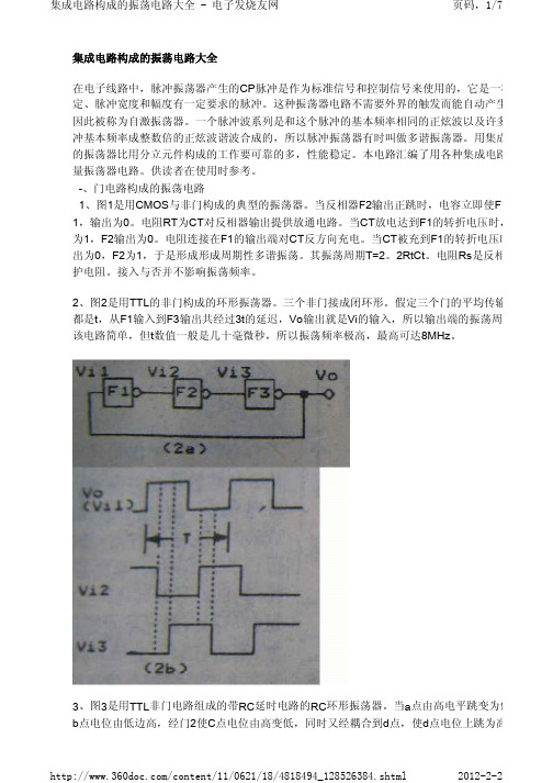
2、图2是用TTL的非门构成的环形振荡器。
三个非门接成闭环形。
假定三个门的平均传输都是t,从F1输入到F3输出共经过3t的延迟,Vo输出就是Vi的输入,所以输出端的振荡周期该电路简单,但t数值一般是几十毫微秒,所以振荡频率极高,最高可达8MHz。
3、图3是用TTL非门电路组成的带RC延时电路的RC环形振荡器。
当a点由高电平跳变为低b点电位由低边高,经门2使C点电位由高变低,同时又经耦合到d点,使d点电位上跳为高以门3输出即e点电位为低。
随着c充电电流减少,d点电位逐渐降低,低到关门电压时门3由低变高,再反馈到门1,使b点由高变低,d点下降到较负的电压值,保证门3输出为高。
使d点上升到开门电压时,门3打开,e点又由高变低,输出电压Vo又回复为低电平,如此交变化形成连续的自激振荡。
振荡周期T=2.2RC。
R可用作频率微调,一般R值小于1k欧姆。
护电阻。
STR7系列微控制器复习课程
S T R7系列微控制器第二章 STR7系列微控制器 (3)2.1STR71X系列微控制器 (3)2.1.1 特点 (4)2.1.2 总体结构 (6)2.1.3 引脚描述 (11)2.1.4 电气特性 (23)2.2STR73X系列微控制器 (29)2.2.1 特点 (30)2.2.2 总体结构 (32)2.2.3 引脚描述 (36)2.2.4 电气特性 (44)第二章 STR7系列微控制器意法半导体(ST)的STR7系列微控制器基于16/32位 ARM7TDMI RISC CPU,该系列种类齐全,用户可以根据不同的应用需求选择合适的芯片。
根据内核类型、片内Flash和片内RAM的容量,以及片上外设资源种类和数量的不同,STR7系列微控制器主要分成如下几类:STR71x系列、STR73x系列以及STR75x系列。
本章将对它们的硬件特性、结构和电气特性作一介绍,更详细的交、直流特性可参考ST的相关数据手册。
片内外设的详细描述可参考本书的第三章。
2.1 STR71x系列微控制器STR71x系列是片上集成Flash和RAM的微控制器系列。
它基于高性能的ARM7TDMI内核,拥有丰富的外设和增强的I/O功能。
该系列中的所有器件都包含片上高速单电压Flash存储器和高速RAM存储器。
由于内嵌ARM内核,所以STR71x与所有的ARM工具和软件兼容。
表2.1-1是STR71x系列微控制器器件型号总览,可作为选型参考。
表2.1-1 STR71x器件总表2.1.1 特点1.存储器✓片内集成最高达256+16k字节的flash存储器(代码FLASH可反复擦写10,000次,数据FLASH可反复擦写100,000次,存储信息最长可以保持20年),可加密保护;✓片内集成最高达64k字节的RAM存储器;✓拥有可以寻址4个存储器段的外部存储器接口(EMI),支持SRAM、Flash 以及ROM等存储器类型;✓支持多种启动方式。
《振荡器的设计》PPT课件

调制频率越低,调频噪声越大。
1. 调频噪声
可
( 2)均方根频偏
整
调 频 噪 声 也 可 以 用 频 偏 直 接 表 示 , 即 采 用 均 方 根 理频
偏 frms 表 示 调 频 噪 声 , 它 是 单 位 带 宽 噪 声 边 带 对 应 的p频pt
偏 均 方 值 。 frms 的 数 值 由 下 式 表 示
振荡器主要技术指标—调频噪声和相位噪声 可
整
在振荡器电路中,由于存在各种 不确定因素的影响,使振荡频率
理
和振荡幅度随机起伏。
ppt
振荡频率的随机起伏称为瞬时频 率稳定度,频率的瞬变将产生调 频噪声、相位噪声和相位抖动。 振荡幅度的随机起伏将引起调幅 噪声。因此,振荡器在没有外加 调制时,输出的频率不仅含振荡
ppt
2.相位噪声
– (1)相位噪声的定义
– (2)相位噪声的表示法 • ①相位脉动谱密度
• ②频率脉动谱密度
• ③单边带相位噪声谱密度
3.频谱纯度
1. 调频噪声
可
( 1) 功 率 表 示
整
理 调 频 噪 声 可 以 用 离 载 频 f0 为 fm 处 的 单 位 频 带 调 频 噪 声 功 率 P n 与 载 波 功 率
图8-1 振荡器输出的频谱
频率f0,在f0附近还包含许多旁频,连续分布在f0两边。如图8-1 所示,纵坐标是功率,f0处是载波功率(振荡器输出功率),f0 两边的是噪声功率,它同时包含调频噪声功率和调幅噪声功率。
振荡器主要技术指标—调频噪声和相位噪声 可
整
1.调频噪声
理
– (1)功率表示 – (2)均方根频偏
1.介质谐振器
可
(1)微波介质谐振器
- 1、下载文档前请自行甄别文档内容的完整性,平台不提供额外的编辑、内容补充、找答案等附加服务。
- 2、"仅部分预览"的文档,不可在线预览部分如存在完整性等问题,可反馈申请退款(可完整预览的文档不适用该条件!)。
- 3、如文档侵犯您的权益,请联系客服反馈,我们会尽快为您处理(人工客服工作时间:9:00-18:30)。
AN2867Application noteOscillator design guide for ST microcontrollers简介:大部分设计人员对振荡器(Pierce-Gate topology 皮尔斯门结构)都很熟悉,但真的明白它是如何工作的人并不多,更甭提设计一个合适的振荡器了。
实际上,很多设计人员并未真正关注过振荡器的设计,直到他们发现振荡器不正常运行了(通常这时产品已经投产了)。
这本是不应该发生的。
许多系统、工程项目的拖延就仅仅是因为一个振荡器没有工作在预计的状态上。
振荡器应该在产品设计阶段就得到足够的重视,并且最好是在投产之前。
这样设计人员才可能避免大批产品被退回来返修那噩梦样的场景。
本应用笔记将介绍皮尔斯(Pierce)振荡器的基本原理,并为如何设计一个优良的振荡器提供指导。
同时也会说明如何选取不同的外围元件,并就怎样为振荡器设计一个优良的PCB提供指导。
本文档的最后部分就如何选取合适的晶体和外围元件提供一个简单的指导,并列出一些为STM32和STM8A/S推荐的晶体型号(HSE和LSE),以方便快速开始一个设计。
1.石英晶体的特性和模型(Quartz crystal propertiesand mod el)石英晶体是一种压电器件,它能够实现电能和机械能的互相转换。
这个转换发生在谐振频率处。
石英晶体的等效模型如下:Figure 1. Quartz crystal modelC0:代表电极引入的并联电容L m:(振荡电感)代表晶体的振荡量C m:(振荡电容)代表晶体的振荡弹性R m:(振荡电阻)代表电流损耗晶体的阻抗计算式如下:(假设R m是可以忽略的)图2是晶体在频域内的阻抗曲线。
Figure 2. Impedance representation in the frequency domainF s是晶体在Z=0时的串联谐振频率。
它的表达式可以从等式(1)中推导出来:F a是反谐振频率,此时的Z趋于无穷大。
从等式(1)中可以推导出它的表达式为:由Fs和Fa界定的区域被称作为并联谐振区域(图2中的阴影部分)。
在这段区域内,晶体工作在并联谐振状态下,其表现像一个电感,会在环路中增加180度的相移。
它的频率Fp(或F L:负载频率)的表达式如下:从等式4中可以看出,晶体的振荡频率能够通过使用不同的负载电容C L进行调校。
这也就是为什么晶体制造商会在他们的晶体数据手册内指明晶体振荡在标定的频率上时所需要的精确的负载电容C L值。
表1给出了一个标定为8MHz的晶体,其等效电路元件值的例子。
表1 等效电路的参数的例子通过等式(2)、(3)、(4)我们可以算出这个晶体的Fs,Fa,Fp:Fs = 7988768 Hz,Fa = 8008102 Hz如果该晶体电极上的负载电容C L等于10pF,则该晶体将振荡在如下的频率上:Fp = 7995695 Hz如果要精确的得到8MHz的振荡频率,则C L应等于4.02pF。
2.振荡器理论一个振荡器包含一个放大器和一个提供选频的反馈网络。
图3是这个基本原理的框图:图3 振荡器原理●A(f) 是放大器的复转移函数(complex transfer function),为保持振荡器的振荡提供能量。
●B(f) 是反馈的复转移函数(complex transfer function),用来设置振荡器的频率。
为了能够振荡,必须要满足以下Barkhausen条件:闭环增益大于1;总相移为360度。
即:启动振荡器需要有一个初始的电能量。
上电的瞬间以及噪声都可以提供这种能量。
但是,这个能量必须足够大到可以触发振荡器振荡在设计的频率上。
数学表达式为:这个表达式意味着开环增益必须远大于1。
振荡器达到稳定所需要的时间就取决于这个开环增益。
满足了振荡条件并不足以解释晶体振荡器为什么可以起振。
实际上,之所以能够起振,是因为在满足了振荡条件后,那个放大器是非常不稳定的,从正反馈网络中引入的任何一点干扰都会导致放大器的失稳并导致起振。
这个干扰可以归因于一个上电,一个使能电平的跳变,或者是晶体的热噪声,等等。
另外值得注意的是,只有落在串-并频率范围内的噪声能够被放大(译注:“串-并频率范围”是指图2中Fa到Fs之间的频率)。
这表示能够触发振荡的频率范围是很小的,这也就解释了为什么晶体振荡器需要如此长的时间才能启动。
3.皮尔斯振荡器(Pierce oscillator)皮尔斯振荡器(Pierce oscillator)在各种应用中使用的非常普遍,因为它功耗低,成本低,并且稳定性好。
图4 皮尔斯振荡器(Pierce oscillator)电路Inv:内部的反向器,作为放大器来工作。
Q:石英晶体或者陶瓷谐振器。
R F:内部反馈电阻。
R Ext:外部电阻,用于限制反向器的输出电流。
C L1和C L2:两个外部负载电容。
Cs:MCU引脚(OSC_IN和OSC_OUT)间和PCB线路上的杂散电容,它是一个并联电容。
4.皮尔斯振荡器的设计(Pierce oscillator design)本章讲解各种限定因素,以及如何为它们取值,进一步熟悉皮尔斯振荡器(Pierce oscillator)的设计。
4.1 反馈电阻RF(Feedback resistor RF)在大多数的ST微控制器中,R F是嵌入在振荡器电路内部的,它的作用是使反向器作为放大器工作。
该反馈电阻被并接在Vin和V out上,这样就使放大器的V out = Vin,从而强制它运行在线性区内(图5中的阴影区域)。
放大器会把处于串-并频率范围(Fa,Fs)(译注:原文为(Fa, Fa),应是有误)内的噪声放大(例如,晶体的热噪声)。
这个噪声会引发振荡器起振。
在某些情况下,当振荡器的振荡稳定后将R F移走,振荡器仍可以继续正常的运行。
图5 反向器的转移函数表2是R F的典型值。
表2 在给定的频率下的典型R F值4.2 负载电容CL (Load capacitor CL)负载电容是指与晶体振荡器相连的电路中的所有电容。
它的值取决于外接电容C L1、C L2,以及PCB和连接点上的杂散电容(Cs)。
负载电容C L由晶体制造商指定。
值得注意的是,若要得到精确的频率,振荡器电路的负载电容必须与所需要的值相等;若要频率保持稳定,则负载电容必须稳定。
外接电容C L1和C L2就是为了把负载电容调校为制造商所指定的C L值。
下面的等式给出了负载电容C L的表达式:下面举一个例子说明外接电容C L1、C L2的值的计算:假设某晶体的负载电容C L值为15pF,且Cs=5pF,则:4.3 振荡器的增益裕量(Gain margin of the oscillator)增益裕量是一个关键参数,它决定着振荡器是否能够起振。
它的表达式是:其中,●g m是反向器的跨导(在高频模块中的单位是mA/V,在32KHz低频模块中的单位是μA/V)●g mcrit(g m 的临界值),取决于晶体的参数。
假设C L1 = C L2,并且晶体上的负载电容与制造商的给定值完全一样,则g mcrit可用下式来表示:,式中ESR的意思是等效串联电阻(equivalent series resistor)根据Eric Vittoz理论:晶体动态的等效RLC电路的阻抗由放大器和两个外接电容的阻抗作补偿。
由此理论,反向器的跨导(gm)的值必须满足g m> g mcrit,这是振荡器能够正常运行的必要条件。
通常认为,增益裕量值为5是保证振荡器有效起振的最小值。
举个例子,为某微控制器中g m值为25 mA/V的振荡器做设计时,我们选择了具有以下特性的石英晶体:frequency = 8 MHz,C0 = 7 pF,C L = 10 pF,ESR = 80,问此晶体是否可以用于此微控制器?我们首先计算一下g mcrit,然后计算gain margin,可见,gain margin值远大于5,满足起振条件,能够起动振荡器。
晶体能够正常振荡。
如果计算后发现gain margin值不合适(增益裕量gain margin值小于5),则达不到振荡条件,晶体将不能振荡。
这时你只能再选择一个有更低ESR和/或有更低C L值的晶体了。
4.4 驱动功率和外接电阻的计算(Drive level DL and external resistor R Ext calculation)驱动功率与外接电阻紧密相关,因此在本章中将两者一并讨论。
4.4.1 计算驱动功率(Calculating drive level DL)驱动功率就是指晶体内消耗的功率。
它必须被限制在一定范围内,否则晶体会因过度的机械振动而损坏。
最大驱动功率由晶体制造商指定,单位通常用mW。
超过指定的驱动功率,可能会导致晶体损坏。
驱动功率可以用这个表达式来表示:其中,●ESR是等效串联电阻(由制造商指定)。
●I Q是流过晶体的电流的有效值(均方根)。
流过晶体的电流可以通过示波器观测到,它是一个正弦曲线。
电流值可以通过测量峰-峰值(I PP)读出。
如果使用电流探针(如图6所示),示波器上电压网格的尺度就可以转换为1mA/1mV 。
图6 使用电流探针测量驱动电流由前面所述的可知,在用电位计调节流过晶体的电流时,电流值不可以超过I Q max的有效值(均方根)(假设流过晶体的电流是完全正弦的)。
由此,可以反推出I Q max:(译注:I Q maxPP为正弦波的峰-峰值,为求有效值I Q max,需先将峰-峰值除以2,再除以。
交流电有效值的推导过程:原理是总功耗相等,即,假设电阻R=1Ω,单位正弦电压峰值为1V,对正弦电压求平方,再求其周期内的积分得,得到。
)流过晶体的电流值(从示波器上读到的峰-峰值)不可以超过最大峰-峰值电流I Q maxPP,由上式可以得到其最大值为:因此,当实际电流I Q超过了I Q maxPP时,需要加上一个外接电阻R Ext(参考4.4.3节)。
这时该电阻是电路中不可缺少的一部分,相应地,在计算I Q max 的表达式中会增大那个ESR的值。
4.4.2 另一种测量驱动功率的方法(Another drive level measurement method)驱动功率可以按下式计算:其中,I QRMS是交流电流的有效值(均方根)。
电流值可以通过使用一个低电容值(不大于1pF)的示波器探针测量放大器输入端的电压波形计算得出。
因为相对于C L1而言,流入放大器的电流稍不足道,所以我们可以假设流过晶体的电流等于流过C L1的电流。
因此,这一点上的电压有效值(均方根)与电流有效值(均方根)的关系为:(译注:电容阻抗z=1/(2*pi*F*C);所以电流I=V/z可推出上式。