
NCP1271D65R2G 笔记本适配器AC-DC电源管理芯片
NCP1271
Soft-Skipt Mode Standby PWM Controller with Adjustable Skip Level and External Latch
The NCP1271 represents a new, pin to pin compatible, generation of the successful 7−pin current mode NCP12XX product series. The controller allows for excellent stand by power consumption by use of its adjustable Soft−Skip mode and integrated high voltage startup FET. This proprietary Soft−Skip also dramatically reduces the risk of acoustic noise. This allows the use of inexpensive transformers and capacitors in the clamping network. Internal frequency jittering, ramp compensation, timer−based fault detection and a latch input make this controller an excellent candidate for converters where ruggedness and component cost are the key constraints.
Operating Junction Temperature Range
Maximum Storage Temperature Range
ESD Protection Human Body Model ESD Pins 1−6 Human Body Model ESD Pin 8 Machine Model ESD Pins 1−4, 8 Machine Model ESD Pins 5, 6 Charged Device Model ESD
*For additional information on our Pb−Free strategy and soldering details, please download the ON Semiconductor Soldering and Mounting Techniques Reference Manual, SOLDERRM/D.
Rating
Symbol
Value
Unit
VCC Pin (Pin 6) Maximum Voltage Range Maximum Current
Skip/Latch, FB, CS Pin (Pins 1−3) Maximum Voltage Range Maximum Current
Drv Pin (Pin 5) Maximum Voltage Range Maximum Current
Stresses exceeding Maximum Ratings may damage the device. Maximum Ratings are stress ratings only. Functional operation above the Recommended Operating Conditions is not implied. Extended exposure to stresses above the Recommended Operating Conditions may affect
HV Pin (Pin 8) Maximum Voltage Range Maximum Current
Power Dissipation and Thermal Characteristics Thermal Resistance, Junction−to−Air, PDIP−7, Low Conductivity PCB (Note 3) Thermal Resistance, Junction−to−Lead, PDIP−7, Low Conductivity PCB Thermal Resistance, Junction−to−Air, PDIP−7, High Conductivity PCB (Note 4) Thermal Resistance, Junction−to−Lead, PDIP−7, High Conductivity PCB Thermal Resistance, Junction−to−Air, SO−7, Low Conductivity PCB (Note 3) Thermal Resistance, Junction−to−Lead, SO−7, Low Conductivity PCB Thermal Resistance, Junction−to−Air, SO−7, High Conductivity PCB (Note 4) Thermal Resistance, Junction−to−Lead, SO−7, High Conductivity PCB
−0.3 to +500 100
142 57 120 56 177 75 136 69
−40 to +150 −60 to +150
2000 700 200 150 1000
V mA
V mA
V mA
V mA
°C/W °C/W °C/W °C/W °C/W °C/W °C/W °C/W
°C °C
V V V V V
GND
8 HV
6 VCC 5 Drv (Top View)
ORDERING INFORMATION
See detailed ordering and shipping information in the package dimensions section on page 19 of this data sheet.
SOIC−7 D SUFFIX CASE 751U
MARKING DIAGRAMS
8
1271x ALYWG
G 1
8 1
PDIP−7 VHVIC P SUFFIX CASE 626B
1
1271Pxxx AWL
YYWWG
x
= A or B
A= 65 kHz
B= 100 kHz
xxx = Device Code: 65, 100
© Semiconductor Components Industries, LLC, 2009
1
September, 2009 − Rev. 6
Publication Order Number: NCP1271/D
NCP1271
AC Input
EMI Filter
*Optional
latch input*
Rskip
skip/latch HV
FB
CS
Vcc
Gnd Drv
NCP1271
Rr*amp
Figure 1. Typical Application Circuit
+
Output Voltage
−
2
NCP1271
MAXIMUM RATINGS (Notes 1 and 2)
Overtemperature Protection
• Frequency Jittering for Softened EMI Signature • +500 mA/−800 mA Peak Current Drive Capability • Sub−100 mW Standby Power can be Achieved • Pin−to−Pin Compatible with the Existing NCP120X Series • This is a Pb−Free Device
for a JEDEC 51 high conductivity test PCB. Test conditions were under natural convection or zero air flow.
Typical Applications
• AC−DC Adapters for Notebooks, LCD Monitors • Offline Battery Chargers • Consumer Electronic Appliances STB, DVD, DVDR
For Inquiry and buy this part: 86 18664987025
a JEDEC 51 low conductivity test PCB. Test conditions were under natural convection or zero air flow. 4. As mounted on a 40x40x1.5 mm FR4 substrate with a single layer of 650 mm2 of 2 oz copper traces and heat spreading area. As specified
A
= Assembly Location
L, WL = Wafer Lot
八脚电源管理芯片通用型号

八脚电源管理芯片通用型号
200A6 200D6 203D6 DAP02A DAP08A DAP02ALSZ 通用
液晶品牌与型号电源管理芯片型号与封装可代换型号
BENQ 71G+ 1200AP40 直插 1200AP10 1200AP60
AOC 712SI EA1532A贴片
三星型号忘记 DM0565R
优派型号忘记 TOP245YN
LG型号忘记 FAN7601
飞利浦170s6 dap02alsz 贴片(2楼说的)
LG型号忘记 FAN7601 可以用LAF0001代
飞利浦170s6 dap02alsz=sg6841
HP17驱动高压电源全一体 SG5841SZ贴片,可用SG6841DZ 代用。
联想后来出的像IBM的17的,SG6841DZ 可用SG6841D代用(我亲自试过的)
三星型号忘记 DM0565R(有好几款都采用这一个PWM IC的)三星型号忘记 DM0465R(我记得还有这么一款的,
其他我知道的常用型号有
SG6841DZ 贴片很多机器上用到
SG5841SZ 贴片用SG6841DZ可以代用,
DAP8A 与203D6可代用(我没试过)
还有LD7575可用203D6代用,只是1脚的对地电阻不同,LD7575是100K,203D6是24.1K,LP7552可用SG6841代用
DAP02ALSZ与SG6841S可以互换。
[整理版]CQ1265电源模块原理与维修
![[整理版]CQ1265电源模块原理与维修](https://360docs-1393072327.cos.ap-beijing.myqcloud.com/4210e534182e453610661ed9ad51f01dc281571c.webp)
CQ1265电源模块原理与维修A、一次供电和二次供电电路开机后,300V直流电压直接通过VD821(IN4007)半波整流、R821(2W/120欧)电阻降压、给C822(50V/47UF)充电,当CQ1265的3脚电压升到14V 时,电源芯片内部电路开始工作,芯片内部的MOS管开始导通和截止,这个时候就不在由R821支路进行提供工作电压,而是改为由辅助绕组经电阻R824 (0。
5W/10欧)、二极管VD824(AU01Z)整流、电容C822(50V/22UF)滤波,电阻R803(0。
25W/680欧)降压、二极管VD810(18V)钳位)、电容C822(50V/47UF)滤波给CQ1265的3脚提供工作电压,当3脚电压降低到10V时,芯片内部停止工作,内部MOS管也就停止了开关。
B、稳压电路正常工作时,当由于某种原因造成+B电压升高后,通过电阻R852A、R854、R854A、R855、R855A分压到V826(TL431)的1脚(也就是G极)的电压也随之升高,V826是一个基准电压为2。
5V的022U)的充电电流减少,4脚电压降低,芯片内部对应的比较器上电压就降低,比较器的另一个脚接到MOS管另一个源极取样电阻Rsense上(如上图),因此当4脚电压降低就是开关管漏极电流降低电流的降低,也就是开关管提前进入截止状态从而使得+B电压降低;反之就升高。
s5mudu65z00002012-5-20 15:00:15 000C、同步电路电路中的VD825(AU01Z)、R826(4/1W680欧)、C825(1500P)、VD823(IN4148)、R825 1/4W470欧为CQ1265的5脚(SYNC)送入同步信号[幅度一般在9V左右的脉冲电平]。
R825 和R826分压调整电平幅度,R826与C825调整延迟的时间,开关管由导通状态什么时候截止,是由4脚的电平高低来决定的,开关管的截止什么时候导通,是由5脚的脉冲电平送到内部比较器上决定的,当开关管截止后,初级绕组是向次级绕组传递能量的(也就是互感),在次级绕组能量释放完后,开关管并不是立即就导通,而是由开关变压器的初级绕组与C821组成的谐振电路,同步电路的作用就是调整延迟同步电平,使串联谐振的电压幅度谐振到最低时才导通。
NCP1216ANCP1252做正激设计应用

NCP1216ANCP1252做正激设计应用正激设计应用是一种广泛应用于电源系统中的设计技术。
在正激设计中,NCP1216A和NCP1252是两款常用的控制器芯片,它们可以实现高效率、可靠性和稳定性的电源系统设计。
NCP1216A是一款可编程的固定频率电源因子校正、切换策略双输出PWM控制器。
该芯片配备了高性能的16位XVID (eXtreme Voltage Interface and Drive) 驱动引脚,可在宽范围的工作电压下实现高达700 VDC的耐压能力。
NCP1216A内置了多种保护功能,如过功率保护、过温保护和过电压保护,以确保电源系统的稳定和安全性。
此外,NCP1216A还具有休眠模式,可在轻载时降低功率消耗。
NCP1252是一款可编程高性能的固定频率电源因子校正PWM控制器。
与NCP1216A相比,NCP1252具有更高的集成度和更强大的功能。
它采用了嵌入I2C总线数字接口和极高的模拟内容,能够有效控制各种类型的电源因子校正。
该芯片还内置了完整的防护机制,如过温保护、过流保护和过电压保护,以确保电源系统的稳定性和可靠性。
在使用NCP1216A和NCP1252进行正激设计应用时,需要先确定电源系统的需求和规格。
这包括输入电压范围、输出电压和电流、负载特性等。
根据这些参数,可以选择合适的NCP1216A或NCP1252芯片,并进行相应的电路设计。
在设计中,需要考虑的几个关键因素包括电感、电容和开关管的选型。
选择适当的电感和电容可以确保电源系统具有良好的抗干扰性和稳定性。
选择合适的开关管可以提供高效率和可靠性。
设计电路时,需要根据NCP1216A或NCP1252的数据手册提供的应用指导和推荐电路来进行。
这些电路包括输入滤波器、电源因子校正电路、PWM控制电路等。
同时,电源系统的布局和连接也需要遵循一定的规范,以确保信号的可靠传输和电子部件的散热。
在设计完成后,需要进行严格的测试和验证。
液晶电源管理芯片代换大全

液晶电源管理芯片代换大全1200AP40 1200AP60、1203P60200D6、203D6 DAP8A 可互代203D6/1203P6 DAP8A2S0680 2S08803S0680 3S08805S0765 DP104、DP7048S0765C DP704加24V的稳压二极管ACT4060 ZA3020LV/MP1410/MP9141ACT4065 ZA3020/MP1580ACT4070 ZA3030/MP1583/MP1591MP1593/MP1430ACT6311 LT1937ACT6906 LTC3406/A T1366/MP2104AMC2576 LM2576AMC2596 LM2596AMC3100 LTC3406/AT1366/MP2104AMC34063A AMC34063AMC7660 AJC1564AP8012 VIPer12AAP8022 VIPer22ADAP02 可用SG5841 /SG6841代换DAP02ALSZ SG6841DAP02ALSZ SG6841DAP7A、DP8A 203D6、1203P6DH321、DL321 Q100、DM0265RDM0465R DM/CM0565RDM0465R/DM0565R 用cm0565r代换(取掉4脚的稳压二极管)DP104 5S0765DP704 5S0765DP706 5S0765DP804 DP904FAN7601 LAF0001LD7552 可用SG6841代(改4脚电阻)LD7575PS 203D6改1脚100K电阻为24KOB2268CP OB2269CPOB2268CP SG6841改4脚100K电阻为20-47KOCP1451 TL1451/BA9741/SP9741/AP200OCP2150 LTC3406/AT1366/MP2104OCP2160 LTC3407OCP2576 LM2576OCP3601 MB3800OCP5001 TL5001OMC2596 LM2596/AP1501PT1301 RJ9266PT4101 AJC1648/MP3202PT4102 LT1937/AJC1896/AP1522/RJ9271/MP1540SG5841SZ SG6841DZ/SG6841DSM9621 RJ9621/AJC1642SP1937 LT1937/AJC1896/AP1522/RJ9271/MP1540STR-G5643D STR-G5653D、STR-G8653DTEA1507 TEA1533TEA1530 TEA1532对应引脚功能接入THX202H TFC719THX203H TFC718STOP246Y TOP247YV A7910 MAX1674/75 L6920 AJC1610VIPer12A VIPer22A[audio01]ICE2A165(1A/650V.31W);ICE2A265(2A/650V.52W);ICE2B0565(0.5A/650V.23W):ICE2B165(1A/650V.31W);ICE2B265(2A/650V.52W);ICE2A180(1A/800V.29W);ICE2A280(2A/800.50W).KA5H0365R, KA5M0365R, KA5L0365R, KA5M0365RN# u) t! u1 W1 B) R, PKA5L0365RN, KA5H0380R, KA5M0380R, KA5L0380R1、KA5Q1265RF/RT(大小两种体积)、KA5Q0765、FSCQ1265RT、KACQ1265RF、FSCQ0765RT、FSCQ1565Q这是一类的,这些型号的引脚功能全都一样,只是输出功率不一样。
笔记本芯片代换
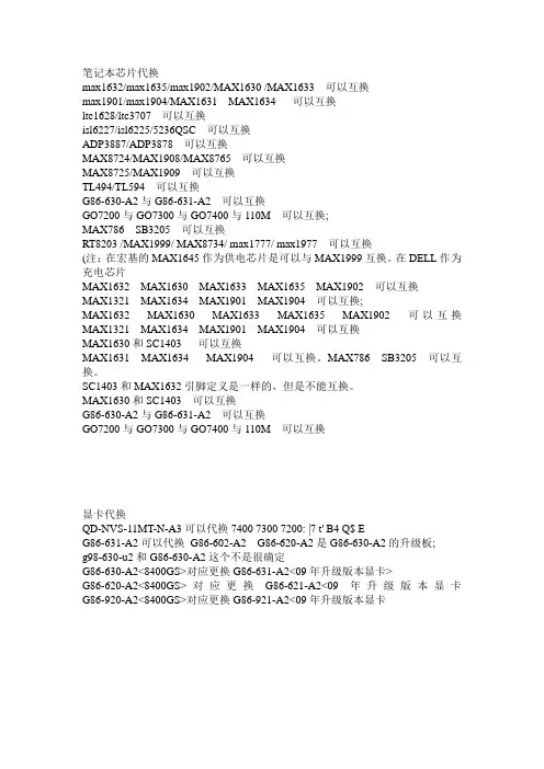
笔记本芯片代换max1632/max1635/max1902/MAX1630 /MAX1633 可以互换max1901/max1904/MAX1631 MAX1634 可以互换ltc1628/ltc3707 可以互换isl6227/isl6225/5236QSC 可以互换ADP3887/ADP3878 可以互换MAX8724/MAX1908/MAX8765 可以互换MAX8725/MAX1909 可以互换TL494/TL594 可以互换G86-630-A2与G86-631-A2 可以互换GO7200与GO7300与GO7400与110M 可以互换;MAX786 SB3205 可以互换RT8203 /MAX1999/ MAX8734/ max1777/ max1977 可以互换(注:在宏基的MAX1645作为供电芯片是可以与MAX1999互换。
在DELL作为充电芯片MAX1632 MAX1630 MAX1633 MAX1635 MAX1902 可以互换MAX1321 MAX1634 MAX1901 MAX1904 可以互换;MAX1632 MAX1630 MAX1633 MAX1635 MAX1902 可以互换MAX1321 MAX1634 MAX1901 MAX1904 可以互换MAX1630和SC1403 可以互换MAX1631 MAX1634 MAX1904 可以互换。
MAX786 SB3205 可以互换。
SC1403和MAX1632引脚定义是一样的,但是不能互换。
MAX1630和SC1403 可以互换G86-630-A2与G86-631-A2 可以互换GO7200与GO7300与GO7400与110M 可以互换显卡代换QD-NVS-11MT-N-A3可以代换7400 7300 7200: |7 t' B4 Q$ EG86-631-A2可以代换G86-602-A2 G86-620-A2是G86-630-A2的升级板;g98-630-u2和G86-630-A2这个不是很确定G86-630-A2<8400GS>对应更换G86-631-A2<09年升级版本显卡>G86-620-A2<8400GS>对应更换G86-621-A2<09年升级版本显卡G86-920-A2<8400GS>对应更换G86-921-A2<09年升级版本显卡。
ncp1271芯片原理

ncp1271芯片原理NCP1271芯片是一种常用的开关电源控制器芯片,具有广泛的应用领域。
本文将介绍NCP1271芯片的工作原理和其在开关电源控制中的应用。
开关电源是一种将输入电压转换为稳定输出电压的电源装置。
在开关电源中,NCP1271芯片起到控制输入电压的稳定输出电压的作用。
它主要通过工作在开关模式下,调整开关管的导通和关断时间,以控制输出电压的稳定性和效率。
NCP1271芯片的工作原理基于PWM(脉冲宽度调制)技术。
当输入电压施加到芯片的电源引脚时,芯片内部的电源管理模块将对输入电压进行整流和滤波。
然后,芯片通过内部的比较器和误差放大器等电路,将输出电压与参考电压进行比较,并生成相应的反馈信号。
NCP1271芯片的控制电路包括一个内部的振荡器和一个PWM控制器。
振荡器产生一定频率的方波信号,PWM控制器根据反馈信号和参考电压的差异,调整方波信号的占空比。
占空比的调整直接影响开关管的导通和关断时间,从而控制输出电压的稳定性。
NCP1271芯片还具有多种保护功能,包括过电流保护、过温保护和短路保护等。
当输出电流超过额定值时,芯片会自动调整开关管的导通时间,以避免过载损坏。
当芯片温度超过允许范围时,芯片会自动降低PWM信号的占空比,以避免过热。
当输出短路时,芯片会自动切断开关管的导通,以保护电路和负载。
NCP1271芯片在开关电源中的应用非常广泛。
它可以用于各种电源类型,包括离线电源和直流-直流转换器等。
在离线电源中,NCP1271芯片可以实现电网电压的稳定输出,广泛应用于家用电器、工业设备和通信设备等领域。
在直流-直流转换器中,NCP1271芯片可以将不同电压等级的直流电源进行转换,用于电动汽车、太阳能电池组和电池充电器等应用中。
NCP1271芯片是一种常用的开关电源控制器芯片,具有高效稳定的特性和多种保护功能。
其工作原理基于PWM技术,通过调整开关管的导通和关断时间,实现对输出电压的控制。
笔记本电脑芯片级维修常用芯片及其功能
笔记本电脑芯片级维修常用芯片及其功能开机芯片: IBM: TB62501F、 TB6805F、 TB62506、 TB6806F、 TB6807F、TB6808F、 BD4175KV 东芝 TMP87PM48U、TMP48U、TMP87PH48U I/O 芯片:PC97338、PC87391、PC87392、pc87393、 SMSC 系列: FDC37N869、FDC37N958、 FDC37N972、 LPC47N227/217、 LPC47N252 LPC47N253、LPC47N254、LPC47N354、LPC47N267 线性稳压块:2951、LP2951、m5236、2950、AAT3200、AAT3680、AME8824、AMS1505、 APL5912、APL5913、G9338、SC1565、MAX8863、MIC5205、SI9183、键盘芯片:H8C/2471、H8/3434、 H8/3431、H8S/2116V、PC87541、PC87570、PC87591 PC87594、PC97551、PC97554 键盘芯片:具有开机功能: H8/3434、 H8/3437、H8/2147、 H8/2149、 H8/2161、 H8/2168、 PC87570、PC87591、H8S/XXX 、M38857、M38867、M38869 系统供电芯片:ISL6228 ISL6232、ISL6235、ISL6236、ISL6237、MAX1630 MAX1631、MAX1632、 MAX1633、 MAX1634、 MAX1635、 MAX17003E、 MAX1901、MAX1902、 MAX1904、 MAX1977、 MAX1999、 MAX785、 MAX786、 MAX8734、MAX8744、 MAX17003、 MAX17004、 LTC1628、 LT3728L、 LT3728LX、SB3052、 SC1402、 SC1403、 SC1404、 SC2450、 TPS51020、 TPS51120 〈 MAX1631、MAX1634、MAX1904 可互换〉〈 MAX1632、MAX1635、MAX1902 可互换〉〈 MAX786、SB3052 可互换_老机型〉〈MAX8734、MAX1999 可互换〉 SC1402 (与 MAX1632 一样)IBM R40 用LTC1628(与 MAX1632 差不多)索尼常用 MAX785、MAX786(奔 2 机器) 辅助供电芯片:ADP3160、ADP3167、ADP3168、APW7057、APW7060ISL6224、ISL6225、 ISL6227、 ISL6236、 ISL6269、 IPM6220A、 MAXl540、MAXl541、 MAX1544、 MAX1549、 MAX1623、 MAX1626、 MAX1627、MAX1644、 MAX1710、 MAX1711、 MAXl712、 MAX1714、 MAX1715、MAX1717、 MAX1718、 MAX1809、 MAX1844、 MAX1845、 MAX1992、MAXl993、MAX8505、MAX8550、MAX8632、MAX8743、MAX8794、SC1470、SC1474、SC1476、 SC1485、SC1486、SCl486A、SC470、SI786LG、G2996、SWC1486、TPS51116、 TPS51117、TPS51120、TPS51124、TPS54610、TPS54672 CPU 供电芯片:ADP3166、ADP3170、ADP3180、ADP3181、ADP3203、ADO3205、ADP3207、 ADP3208、 ADP3209、 ADP3421、 AIC1567、 ISL6215、ISL6217、 ISL6218、 ISL6219、 ISL6223、 ISL6227、 ISL6260、ISL6262、 LTC1436、 LTC1736、 LTC1709、 LTC3716、 LTC3735、MAX1532、 MAX1533、 MAX1710、 MAX1711、 MAX1712、 MAX1714、MAX1717、 MAX1718、MAX1830、MAXl831、MAX1897、MAX1907、MAX1987、MAX1988、MAX798、 MAX8760、MAX8770、MAX8771、MAX8774、SC451、SC452、SC1474、SC1476 供电芯片搭配使用:ADP3203/ADP3415、ADP3205+ADP3415、ADP3410+ADP3421、ADP3410+ADP3422、ADP3207+ADP3419、ADP3208+ADP3419 电池充/放电控制芯片:AAI3680、ADP3801、ADP3806BQ24700、BQ2470l、BQ24702、 BQ24703、BQ24740、DS2770、ISL6251 长和方、ISL6252、ISL6253 长和方、 ISL6256、ISL88731、 M61040FP、 MAXl644 MAX1736 MAX1772、 MAX1773、 MAX1870 MAX1645、 MAX1647、 MAX1648、 MAX745、 MAX1873、 MAX1908、 MAX1909、MAX745、MAX8724、 MAX8725、 MAX8731、 MAX8765、 MB3878、 MB3879、 MB3887、MB39A126PFV、 LT1505G、LTl505、LTC4008、TC490/591、TL494、TL594、OZ983、OZ985、笔记本电池电量检测芯片:BQ2040、BQ2060 CPU 温度控制芯片: MAX1617、 MAX1020A、 AD1020、 AD1021、 AD1030、 AD1030A、AD1031、 CM8500、MAX1989、AD1020A、MAX6654、ADM1032、G781、LM26 网卡芯片: RTL8100、 RTL8139、 Intel-DA82562ET、 RC82540、 3COM、BCM440、 BCM5702KBGA、 88E8001、88E8055、82562EZ 网卡隔离器:LF8423、LF-H80P、H-0023、H0024/42、H0019、ATPL-119(内部是线圈, 非电路) 声卡芯片: ES1921、 ESS1980S、 STAC9704、 AU8810、4299-JQ、 4297-JQ、 AD1885、 AD1984、 8552TS、8542TS、CS4239-KQ、AD1981、AD1981B、ADl888、ADl981、AD1986、ALC200、 ALC201A、ALC202、ALC203、ALC258、ALC262、ALC655、ALC658、ALC660、ALC861、 ALC880、ALC883、CMl9738、CS4205、CX20468、CX20549、CX20561 PT2353、(没声音,杂音,声小,查功放芯片)(开机时,没有声音,无声卡设备,查声卡芯片)音频功放芯片:APA2020、TPA0142、TPA0312、TPA6017、TPA0202、LM4835、LM4838、 LM4861、LM4863、LM4880、LM4881、LM4882、LM4911、MAX9710、MAX9750、 MAX9751、 MAX9755、 MAX9789、 MAX9790、 ESS1980S、8552TS、 8542TS、 TPA0302、 AU8810 、BA7786、AN1294、AN12941、AN12942B、AN12943、G1420 PC 卡信号芯片:R5C551、R5C552、R5C476、R54472、R5C593、SN0301520、PCIXXX、 PC 卡供电芯片:TPS2205、TPS2206、TPS2216、TPS2211、TPS2224、PU2211、M2562A、 M2563A、M2564A、OZ2206、超级 I/O:PC8394T IO 芯片:PC 系列:PC87591S (VPCQ01)、PC 87591L(VPC01)、PC97317IBWPC87393 VGJ、PC87591E-VLB、PC87591E (-VPCI01)/(VPCQ01)、PC97551-VPC、 PC87570-ICC/VPC、PC87391VGJ、PC8394T、PC87392、PC87541L、 PC87541VPC87591E-VLB、TB 系列:TB62501F、TB62506F、TB6808F、 ENE 系列: KB3910QB0、KB910SFC1、 KB3910SF、 KB910QF、 KB910QB4、 KB910LQF、 KB910LQFA1 其它系列:IT8510E、PS5130、W83L950D、LPC47N249-AQQ、PCI4510、LPC47N253-AQQ、 LPC47N250-SD、LPC47N252-SG、LPC47N254-AQQ、(1)管理串口、并口、软驱、I/O:PC97338、MB87392、(2)管理键盘、鼠标、且带开机功能:H8/3437、 H8。
ncp1271芯片原理
ncp1271芯片原理NCP1271芯片是一款高效率、高集成度的PWM控制器,主要用于电源管理应用。
它具有多种保护功能,并且能够提供稳定可靠的电源输出。
本文将介绍NCP1271芯片的工作原理和特点。
一、NCP1271芯片的工作原理NCP1271芯片采用了当前模式PWM控制技术,通过对输入电压和输出电流进行采样,实现对输出电压的精确控制。
它内部集成了一个高精度的误差放大器和一个比较器,用于监测输出电压和参考电压之间的差异。
当输出电压下降时,误差放大器会将其放大,并与参考电压进行比较。
比较器的输出信号将控制PWM控制器的工作周期,以调整输出电压。
NCP1271芯片还具有一个内置的频率抖动功能,用于降低系统噪声。
频率抖动可以使系统中的噪声功率分散到更宽的频率范围内,从而减小噪声对系统性能的影响。
此外,NCP1271芯片还具有过载保护、短路保护和过温保护等多种保护功能,可以有效保护电源系统的安全运行。
二、NCP1271芯片的特点1. 高效率:NCP1271芯片采用了先进的PWM控制技术,能够实现高效率的电源转换,减少能量损耗,提高系统效率。
2. 高集成度:NCP1271芯片集成了多种功能模块,如误差放大器、比较器和PWM控制器等,可以满足复杂电源管理系统的需求,减少外部器件的数量和体积。
3. 多种保护功能:NCP1271芯片具有过载保护、短路保护和过温保护等多种保护功能,可以有效保护电源系统的安全运行,提高系统的可靠性。
4. 频率抖动功能:NCP1271芯片具有内置的频率抖动功能,可以降低系统噪声,提高系统的抗干扰能力。
5. 宽输入电压范围:NCP1271芯片支持宽输入电压范围,可以适应不同的电源输入条件,具有较强的适应性。
6. 精确的输出电压控制:NCP1271芯片通过对输入电压和输出电流的采样,实现对输出电压的精确控制,可以满足对电源输出精度要求较高的应用场景。
三、NCP1271芯片的应用NCP1271芯片广泛应用于各种电源管理系统,如笔记本电脑、平板电脑、服务器、工业设备等。
采用NCP1271设计19V、3.0A通用输入AC-DC适配器
AND8242/D19 V , 3.0 A Universal Input AC−DC Adaptor Using NCP1271Prepared by: Jon Kraft and Kahou Wong ON SemiconductorINTRODUCTIONThe NCP1271 is one of the latest fixed−frequency current−mode PWM switching controllers with (1) adjustable Soft−Skip t standby operation for low−level audible noise, (2) integrated high−voltage startup for saving standby power, (3) timer based overload fault detection, and (4) internal latch protection features. T able 1 summarizes all the features of an NCP1271 based power supply.This application note presents an example circuit (Figure 1) using the NCP1271 (65 kHz version) in a flyback topology. The design steps and subsequent measurements are also included. An Excel based design worksheet is available at .The measurements show that the 19 V , 3.0 A circuit delivers above 85% across a universal input (85 to 265 Vac).The no load standby consumption is 83 mW at 230 Vac and the light load operation is greater than 75% efficient.Figure 1. Application Circuit SchematicAPPLICATION NOTETable 1. Features of Power Supply Using NCP1271Operation Mode FeaturesTopology CCM/DCM Flyback•Fixed−frequency current−mode control with inherent primary current limitation.•Frequency jittering to soften the EMI signature.•Built−in soft−start.•Output short−circuit fault detection independent of the auxiliary winding.•Integrated high voltage startup that minimizes standby power loss.Standby Condition Soft−Skip Operation•Adjustable skip level for optimal standby power consumption.•Proprietary Soft−Skip to reduce the risk of low−frequency audible noise.•Soft−Skip operation is automatically disabled if an abrupt transient load is appliedfrom standby operation. This improves the output response to a transient load.Fault Condition Double HiccupRestart •Double Hiccup operation minimizes the power dissipation in a fault mode and allows the application to auto−recover when the fault is removed.Latch Protection Activated Latch Off•An internal latch makes it easy to add overtemperature protection (OTP) orovervoltage protection (OVP) to any applications.•Latch is reset by unplugging the AC input and allowing V CC to drop below 4 V (typ).The Demo Board SpecificationInput85 to 265 Vac, 50 HzOutput19 Vdc, 3.0 A, IsolatedFeatures•< 100 mW Input Power at 230 Vac•Excellent Light Load Performance•No Audible Noise•> 85% Full Load Efficiency•Short Circuit Protection Activates at < 100Wfor Any Input VoltageA Discontinuous Conduction Mode (DCM) flyback was selected for this application. DCM gives very good stability, small inductor size (lower leakage inductance), and good transient response.Flyback CalculationsSeveral resources are available at to calculate the necessary component values for a flyback supply. In particular, an Excel based design spreadsheet can be found at:/collateral/NCP1271SHEET.xls Additionally, most of the other NCP12xx application notes also apply to the NCP1271. For detailed information on designing a flyback power supply, please visit AND8076/D. Other app notes which may also aid in the design include:AND8069/D Tips and Tricks to Build Efficient CircuitsWith the NCP1200AND8205/D How to Choose a Switching Controller forDesignAND8023/D Implementing the NCP1200 in Low−CostAC/DC ConvertersAND8032/D Conducted EMI Filter Design for theNCP1200AND8076/D A 70 W Low Standby Power Supply with theNCP12xx SeriesBased on the results from the NCP1271 design spreadsheet, the final values for this adapter’s key flyback parameters were calculated to be:Np:Ns = 5:1Lp = 180 m HR CS = 0.3 OhmsIpeak(full load) = 3.5 ASwitch Rating = 6 A, 800 VDiode Rating = 3 A, 100 VRsnubber = 100 k WCsnubber = 10 nFSetting the Short Circuit Protection LevelThe current sense resistor (R CS or R8), provides two functions. First it senses the primary current for current−mode PWM operation. Secondly, it provides the maximum primary current limitation according to equation 1:I p(max)+1VR CS(eq. 1) The short circuit protection activates when the I p(max) current is reached for more than 130 ms (typ). This also corresponds to V FB being greater than or equal to 3 V for 130 ms. Therefore, R CS must be set large enough to ensure that the required peak current can always be delivered, but small enough to meet the short circuit protection requirements. A DCM flyback converter has the following relationship:P out+1ń2L p I p2F SW h(eq. 2) Therefore, for an assumed efficiency of 80%, a peak current of 4 A should trigger the short circuit protection circuitry at 80 W. This corresponds to an R CS value of 0.25 W. This change in R CS may also require that the snubber and transformer be re−calculated to handle this level of peak current during the short circuit fault time. A few iterations of the Excel based NCP1271 design spreadsheet should produce a good starting point for the application’s design.Over Power CompensationFor this demo board, the short circuit protection is activated with an output load of 76 W at 85 Vac and 93 W at 265 Vac. The variation in short circuit power level withinput voltage is due to the propagation delay (Tprop) of the NCP1271. This propagation delay has a more pronounced effect on the power delivered at high line than at low line as shown in Figure 2.Figure 2. Effect of Propagation Delay on the Maximum Power Delivered at High Line and Low LinePeak Primary CurrentI p(max)T propT propThis effect is called “Over Power” because it delivers more power than what is requested by the feedback loop.Specifically, for a DCM flyback system, the total power delivered to the output including the prop delay effect is:P out +12@L p @(I p(max))V bulk ńL p @T prop)2@F sw @h(eq. 3)The NCP1271 has been designed with a very low Tprop (50 ns typ). This minimizes the over power effect. However,if reduced variation is required, then over power compensation can be easily implemented by using one of the circuits shown in Figures 3 and 4.Figure 3. Over Power Compensation by means ofa Resistor to the Bulk VoltageR Figure 4. Over Power Compensation by Modifyingthe Auxiliary Winding TopologyAuxThe circuit in Figure 3 simply modifies the CS setpoint proportional to the HV bulk level. This creates an offset which compensates for the propagation delay. However, this does increase the standby power dissipation. Figure 4 gives another option which results in much lower power dissipation. By altering the position of the Aux winding diode, a new point is created whose voltage is proportional to Vin. The power dissipation is now reduced by a factor of (Np:Naux)2. V alues for Ropp are best found experimentally to give suitable precision for the activation of the short circuit protection.Biasing the ControllerThe NCP1271 includes a high voltage (HV) startup pin (Pin 8) which charges V CC to its operating level. This pin can be directly connected to the high voltage DC bus. Once the device is powered up, an auxiliary winding powers V CC as shown in Figure 5.Figure 5. V CC Biasing SchemeThe range of V CC is from 10 V (min) to 20 V (max). Therefore, the auxiliary winding should be designed to give a level of V CC within this range over all output loads. When the circuit is in standby mode, very few pulses are delivered and the auxiliary level decreases. To provide enough voltage range, a nominal V CC level of 16 V was selected for this application. Additionally, an 18 V (±5%) Zener diode was added externally to protect the controller from abnormally high auxiliary levels. The 16 V bias supply is constructed from a 6:5 turns ratio (19 V:16 V) between the main output and the auxiliary winding.Figure 6 shows the auxiliary supply circuit. A resistor is included to provide the flexibility to redesign the circuit for higher output voltages. Any extra bias voltage greater than 18 V is simply dissipated across the resistor.Figure 6. Auxiliary SupplySoft−Skip AdjustmentWhen the load current drops, the compensation network responds by reducing the peak current. When the peak current reaches the skip peak current level, the NCP1271 enters skip operation to reduce the power consumption. The peak current level at which skip is entered should be set high for good standby power dissipation. However, it also needs to be set low enough that no audible noise occurs during each bunch of skip pulses. To address this need, the NCP1271 has a proprietary Soft−Skip feature which ramps each bunch of pulses. This dramatically lowers acoustic noise and allows a higher skip level to be set for greater power savings. The NCP1271 also allows the designer to select the optimal level of the peak current during skip through a simple resistor from pin 1 to GND. This skip resistor sets the skip level according to equation 4:V skip+I skip R skip(eq. 4) where I skip = 43 m A (typ)The peak current when skip mode is activated can be calculated with equation 5:I peak(skip)+V skip3VI peak(max)(eq. 5) For this demo board, V skip was set to 1.3 V (R skip=30.1 k W). And I peak(max) is 1 V / 0.25 W = 4 A. Therefore,I peak(skip) = 1.7 A.Minimum On Time LimitationThe NCP1271 includes a current sense (CS) Leading Edge Blanking (LEB) filter. The LEB filter blanks out the first 180 ns (typ) of the CS voltage at the beginning of each drive pulse. This helps to prevent a premature reset of the output due to noise. However, this also results in a minimum on time of the device. The duration is equal to the LEB time (180 ns typical) and the propagation delay of logic (50 ns typical). If the application circuit is configured for 0% skip (by connecting Pin 1 to Ground), then that minimum on time duration may result in an abnormally high output voltage during no load conditions. Therefore, it is recommended to set skip to some small value rather than disable it completely. Ramp CompensationThe NCP1271 also incorporates a feature called “ramp compensation.” Ramp compensation is a known mean to cure subharmonic oscillations. These oscillations take place at half the switching frequency and occur only during continuous conduction mode (CCM) with a duty−cycle greater than 50%. To prevent these oscillations, one usually injects between 50 and 75% of the inductor down slope into the CS pin. The NCP1271 generates an internal current ramp that is synchronized with the clock. This current ramp is then routed to the CS pin.Since the flyback design in this app note is well within DCM operation, ramp compensation is not necessary. However, for designs that do run in CCM with the NCP1271, ramp compensation is easy to implement. It only requires one external resistor between Rcs and the CS pin. The value of the ramp resistor to obtain 50% inductor down slope injection can be calculated with the following equation:R ramp+0.50R CSǒ(V out)V f)N PSǓǒLp F sw100m A0.80Ǔ(eq. 6)Maximum Duty Cycle and Ramp CompensationIf the ramp resistor is set too high, the maximum duty cycle will be reduced. But as a long as R ramp is below 10 k W ,this will not be a problem. A typical graph of the maximum duty cycle verses R ramp is shown in Figure 7. However, it is not recommended to try to reduce the maximum duty cycle by the R ramp value because this relationship is not guaranteed by the production tests of the device.Figure 7. Maximum Duty Cycle Characteristics 010203040506070809005101520253035404550R RAMP , RESISTOR (k W )M A X I M U M D U T Y (%)Optional Output OVP LatchThe NCP1271 includes a feature where if Pin 1 is brought above 8.0 V (typ), the part will safely latch off the controller.The controller is reset by unplugging the AC input. This allows for easy implementation of overvoltage (OVP) or overtemperature (OTP) protection.In order to pull the Pin 1 voltage above the latch threshold,a greater than 8.0 V source is needed. That is usually the bias supply voltage V CC . Therefore, to protect Pin 1, a resistor (R limit ) is connected to limit the current below the maximum allowed level. In addition, the internal ESD diode will limit the maximum voltage on Pin 1 to about 10 V .This latch off feature can be configured in a variety of ways. Some of the most popular include using the auxiliary winding to detect an overvoltage and using an NTC resistor to detect an overtemperature condition. A few variations of these circuits are listed in Figures 8 to 11.Figure 8. Simple Latchoff Circuit by BipolarTransistorsFigure 9. Overtemperature Protection Latch with aNTC ThermistorNTCresistorFigure 10. Output Overvoltage Protection Using theAuxiliary WindingOVPFigure 11. Output Overvoltage Protection Using anOptocouplerIt is important to note that when Pin 1 is open it sets the default skip level to 1.2 V. However, in this mode, pin 1 is internally pulled high to the Vskip−reset level (6.5 V typ). This only leaves about 1.5 V of noise margin before the part latches off. Therefore, if a skip level of 1.2 V is desired, then instead of leaving pin 1 open, it is always recommended to place a 28 k W resistor from pin 1 to GND. Then the skip level becomes 1.2 V (28 k W x 43 m A = 1.2 V), and the pin 1 voltage is also 1.2 V. This gives much better noise immunity and reduces the chance of falsely triggering the latch due to noise or leakage current from the external latch circuitry. Additionally, a small capacitor should be added to pin 1 to further increase the noise immunity.HV Pin Protection CircuitWhen the main power is interrupted in the application, the high voltage DC bus may potentially go negative in a short transient period. Since this is directly connected to pin 8, it could create a reverse current out of the HV Pin and could potentially damage the device. There are two easy solutions to this problem. The first is demonstrated in Figure 12. The inserted diode turns on when the HV Pin voltage goes below the V CC biasing voltage. This eliminates the chance of negative voltage on the HV pin. A second method is shown in Figure 13. Here, the inserted resistor limits the negative current to a low level and protects the HV pin. Either option works well, but for this demo board, a diode between V CC and HV was used.Figure 12. Protection Diode for HV PinFigure 13. Protection Resistor on HV Pin Layout ConsiderationFigures 9−10 show the layout of the design. It is a single−layer PCB. As with any power converter, some care must be exercised with the design and layout. The following are some important guidelines.1.Minimize the high−current loop and locate the ICcontroller outside the high−current loop to preventmalfunctioning of the IC internal logic due tostrong magnetic fields from the high current.2.Locate the decoupling capacitors close to thedevice to improve noise immunity.3.Locate the V CC capacitor very close to the deviceto prevent the circuit from entering a UVLO faultcondition because of noise.4.Locate the output voltage sense resistor close tothe output load points.5.Minimize the current sense trace. It can becomeeasily polluted with noise.6.Minimize the distance between the feedbackopto−coupler and controller because this trace isalso easily polluted.7.Minimize the distance between the MOSFET andcontroller because the PCB trace is high frequencyand high current so it can easily pollute other partsof the circuit.Additionally, there are three pins in the NCP1271 that may need external decoupling capacitors.1.Skip/latch pin (Pin 1) – If the voltage on this pin isabove 8.0 V, the circuit enters latch−off protectionmode. Hence, a decoupling capacitor on this pin isessential to improve noise immunity. Additionally,a resistor should always be placed from this pin toGND to prevent noise from causing the pin 1 levelfrom exceeding the latch−off level.2.Feedback pin (Pin 2) – A small capacitor may benecessary here for improved stability and noiseimmunity.3.V CC pin (Pin 6) – The NCP1271 maintains normaloperation when V CC is above V CC(off)(9.1 Vtypical). If V CC drops below V CC(off), then thecircuit enters UVLO protection and restarts after adouble hiccup. Therefore, if V CC inadvertentlydrops below V CC(off)due to switching noise, thenthe circuit will recognize it as a fault condition.Hence, it is important to locate the V CC capacitorand a ceramic decoupling capacitor as close aspossible to the NCP1271.MeasurementsStandby PerformanceThanks to the features in the NCP1271, the demo board power supply offers excellent no load and light load standby performance. The 230 V ac power consumption of the 57 W circuit is only 83 mW. And the input power at 230 Vac with 500 mW load is only 710 mW. Figure 14 shows the efficiency with output loads from 500 mW to 60 W at 120 Vac and 230 Vac.Figure 14. Efficiency of the NCP1271 Demo Board atNominal Line Voltages P out (W)605040302060657075808590E F F I C I E N C Y (%)1095Dynamic StudyFigure 15 shows the startup transient waveforms of the circuit when the input is 110 Vac. A 4 ms soft−start is observed in the drain current. The V FB drops below 3.0 V after 32 ms. Since this is shorter than the 130 ms fault validation time, the circuit does not enter fault condition and starts up normally.Figure 15. Startup TransientV outV CCV fbV CSFigure 16 shows the go−to−standby transition from full load operation. The output voltage (yellow trace) does not consume current and remains at 19 V , but the V CC voltage drops from 16 V to 15 V because the V CC auxiliary winding is not supplying current to the controller. The minimum V CC voltage in the transition can be as low as 12 V . This is why the 16 V biasing voltage was selected to maintain V CC above V CC(off) and prevent a V CC reset.Figure 16. Operating to StandbyV outV CCV CSShort Circuit Protection MeasurementsFigure 17 details the operation of the short circuit protection . The load steps from 60 W to 100 W, causing the peak current to increase to its maximum (1 V) as shown by the blue CS voltage. After approximately 130 ms, the controller shuts the power supply down and enters double hiccup fault operation (Figure 18). This provides very low power dissipation and protects the power components.When the short circuit fault is removed, the application recovers by executing a soft start and bringing the output back to 19 V .Figure 17. Short Circuit Protection is Activated Whenthe Output Load Increases to about 100 WV out V CSV CCFigure 18. The Controller Enters Double Hiccup Fault Operation during a Continuous Short Circuit EventV CSV out V CCConclusionA 57 W flyback power supply featuring over voltage and short circuit protection using the NCP1271 was demonstrated to have excellent light load power dissipation and active mode efficiency. The NCP1271’s proprietary Soft−Skip t operation offers low−audible−noise and excellent standby performance. The NCP1271 design worksheet, as well as other design aid resources, are available at .Appendix I: Bill of Materials for the NCP1271 19 V/3.0 A Example CircuitDesignator Qty Part Number Description Manufacturer T11E3506−A 3.0 A 508 m H Common−Mode Filter CoilcraftCooper/Coiltronics T21CTX22−17179Custom Transformer 180 m H 30:6:5,2.5 m H Max LeakageIC11NCP1271D65R265 kHz Flyback PWM Controller, SO−7ON Semiconductor IC21TL431AID 2.5 V 1% Voltage Reference, SO−8ON Semiconductor IC3–IC42SFH615AA−X007Optocoupler VishayD1–D441N5406 3.0 A 600 V Diode, Axial 267−05ON Semiconductor D51MMSZ914 1.0 A 100 V Diode, SOD−123ON Semiconductor D61MRA4005T3 1.0 A 600 V Diode, SMA ON Semiconductor D71MURS160 1.0 A 600 V Diode, SMB ON Semiconductor D81MBR3100 3.0 A 100 V Schottky Diode, Axial 267−05ON Semiconductor D101MZP4746A18 V @ 14 mA Zener Diode ON Semiconductor Q11SPP06N80C3 6.0 A 800 V N−MOSFET, TO−220AB InfineonR11P100KW−2BK100 k W 2.0 W, Axial 5%−R21CFR−25JB−10R10 W, 1/4 W Axial YageoR51CRCW12063012F30.1 k W, 1206VishayR61CRCW120610R0F10 W, 1206VishayR71CRCW12065110F511 W 1206VishayR81WSL2512R2500FEA0.25 W 1.0 W 1%Vishay R9, R101CRCW12061691F 1.69 k W, 1206VishayR111CRCW12061582F15.8 k W, 1206VishayR121CRCW12062371F 2.37 k W, 1206VishayC1−C22PHE840MA6100MA040.1 m F X2 Cap 10 mm Pitch Evox RifaC31ECOS2GP820BA,82 m F 400 V Electrolytic PanasonicEETED2G820BA, orEETXB2G820BAC4, C132ECA1EM101100 m F 25 V Electrolytic Panasonic C51630MMB103J10 nF 630 V Film Cap Rubycon C6−C71VJ1206Y122KXXA 1.2 nF 25 V, 1206VishayC9–C103025YXG220M12.5X302200 m F 25 V Electrolytic RubyconC111ERO610RJ4100M 1.0 nF 1.0 kV 5.0 mm Pitch Y2 Cap Evox RifaC121VJ1206Y154KXXA0.15 m F 25 V Ceramic VishayFuse11025TD2−R250 V 2.0 A Tie Delay Fuse Cooper Fuse Heatsink1590302B03600Heatsink for TO−220 Package Aavid Heatsink Insulation14672TO−220 Mica Insulation Keystone AC Connector1770W−X2/10IEC60320 C8 Connector Qualtek DC Connector126−60−4030 or 0096520383−T erminal 3.96 mm Pitch Male Header Molex Standoff44804 K Standoff M/F Hex 4−40 Nyl 0.750”−Heatsink Mechanic130F6984−40 1/4 Inch Screw−Heatsink/Standoff531F21064−40 Screw Nuts−MechanicNylon Washer13049Nylon Shoulder Washer #4−Appendix II: NCP1271 57 W Adaptor LayoutFigure 19. Top ViewFigure 20. Bottom ViewON Semiconductor and are registered trademarks of Semiconductor Components Industries, LLC (SCILLC). SCILLC reserves the right to make changes without further notice to any products herein. SCILLC makes no warranty, representation or guarantee regarding the suitability of its products for any particular purpose, nor does SCILLC assume any liability arising out of the application or use of any product or circuit, and specifically disclaims any and all liability, including without limitation special, consequential or incidental damages.“Typical” parameters which may be provided in SCILLC data sheets and/or specifications can and do vary in different applications and actual performance may vary over time. All operating parameters, including “Typicals” must be validated for each customer application by customer’s technical experts. SCILLC does not convey any license under its patent rights nor the rights of others. SCILLC products are not designed, intended, or authorized for use as components in systems intended for surgical implant into the body, or other applications intended to support or sustain life, or for any other application in which the failure of the SCILLC product could create a situation where personal injury or death may occur. Should Buyer purchase or use SCILLC products for any such unintended or unauthorized application, Buyer shall indemnify and hold SCILLC and its officers, employees, subsidiaries, affiliates,and distributors harmless against all claims, costs, damages, and expenses, and reasonable attorney fees arising out of, directly or indirectly, any claim of personal injury or death associated with such unintended or unauthorized use, even if such claim alleges that SCILLC was negligent regarding the design or manufacture of the part. SCILLC is an Equal Opportunity/Affirmative Action Employer. This literature is subject to all applicable copyright laws and is not for resale in any manner.Soft−Skip is a trademark of Semiconductor Components Industries, LLC (SCILLC).PUBLICATION ORDERING INFORMATION。
笔记本维修常用芯片引脚说明
TPS51125 RT8205
16脚VIN 13脚EN0
1、悬空时打开线性供电,准备打开 VCLK和PWM 2、通过620K电阻到GND,打开线性供 电,关闭VCLK和准备开启PWM 3、直接接地,关闭所有输出
RT8206 ISL6236 ISL6237 SN0608098 TPS51427 PM6686
1、大于2V打开线 性供电
常用待机
常用待机芯片
PWM开启 引脚解释
1脚 ENTRIP1 2脚 ENTRIP2
通道1和通道2的开启和过流设定脚 1、直接接地,关闭PWM 2、通过电阻到地,作为电流极限设定
高电平开启(大于2.5V),低电平关闭 14脚EN1 (小于0.8V),当EN1连接REF时,PWM1会 27脚EN2 在PWM2稳定后延时开启,当EN2连接到REF
把ENC置高(大于2V)开启两路PWM 把ENC接地(小于0.6V)关闭两路PWM
21脚EN1 高平开启(大于2.3V) 4脚EN2 低电平关闭(小于0.8V)
4脚EN3 高电平开启(大于2.4V) 25脚EN5 低电平关闭(低于0.8V)
基准电压、线性电压、 PWM内核供电的关系
VIN和EN0正常后,先开启VREF,再产生线性电 压,(根据内部框图判断)
6脚VIN
4脚EN_LDO
高电平(大于1.6V)开启REF和LDO 低电平(小于1V)关闭REF和LDO
MAX8734 MAX8732 MAX8733 MAX1999
20脚V+
6脚SHDN#
高电平(大于1.6V)开启芯片 低电平(小于1V)关闭芯片
TPS51120
22脚VIN
9脚EN5 10脚EN3