升压芯片之RT9212
CMT2119B 高功率 Sub-1GHz 射频发射器说明书
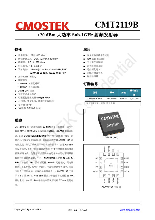
+20 dBm 大功率Sub-1GHz 射频发射器特性 ⏹ ⏹ ⏹ ⏹ ⏹ ⏹ ⏹ ⏹ ⏹ ⏹ ⏹ ⏹ ⏹ 应用于QFN16 (3X 3)17GNDCSB FCSB X IX OG P I O 2G P I O 1NC NC 13141516121112目录1.电气特性 (4)1.1推荐运行条件 (4)1.2绝对最大额定值 (4)1.3功耗 (5)1.4发射机 (5)1.5稳定时间 (6)1.6频率综合器 (6)1.7低电压检测 (6)1.8晶体 (7)1.9低频振荡器 (7)1.10数字接口 (7)1.11典型参数图表 (8)2.管脚描述 (10)3.典型应用原理图 (11)4.功能描述 (12)4.1发射器 (12)4.2辅助模块 (12)4.2.1晶体振荡器 (12)4.2.2睡眠计时器 (13)4.2.3低电压检测 (13)4.2.4快速手动跳频 (13)5.芯片运行 (14)5.1SPI接口 (14)5.2FIFO (14)5.2.1FIFO 读操作 (14)5.2.2FIFO 写操作 (15)5.2.3FIFO 相关中断 (15)5.3工作状态,时序及功耗 (16)5.3.1启动时序 (16)5.3.2工作状态 (16)5.4GPIO和中断 (18)6.数据包及包处理机 (20)6.1数据包格式 (20)6.2数据模式 (20)6.2.1直通模式 (21)6.2.2包模式 (21)7.自动运行模式 (22)8.用户寄存器 (23)8.1CMT区 (23)8.2系统区 (24)8.3频率区 (24)8.4数据率区 (24)8.5基带区 (25)8.6发射区 (25)8.7控制1区 (25)8.8控制2区 (26)9.订购信息 (27)10.封装信息 (28)11.顶部丝印 (29)11.1CMT2119B顶部丝印 (29)12.其它文档 (30)13.文档变更记录 (31)14.联系信息 (32)1. 电气特性V DD = 3.3 V,T OP = 25 °C,F RF = 433.92 MHz。
第二代超级芯片UOC-Ⅱ(S系列)电路分析与维修.doc

第二代超级芯片UOC-Ⅱ(S系列)电路分析与维修康佳第二代超级芯片电视机T2975S、T2976S、P2971S/P2960S、T2173S、P2171S/P2572S、T2576S、P2571S、P2571SR/P2971SN、T2975SR、P2961S、T3476S等“S”系列。
新的“S”系列较“K”系列又增加了一些功能,如“屏保”功能、“时钟”功能、“日历”功能、“色温”功能、“计算器”功能、“游戏”功能、“绿屏”功能等。
扫描速度调制功能的效果更为明显,“S”系列中的“P”(镜面管)机设有实时时钟IC(N105)和地磁校正电路。
与“K”系列相比主要区别在于超级芯片本身,K系列采用的是菲力浦公司的TDA9383,其供电则由N903(TDA8133)电压转换器,将输入的+12V转换成+5V和+8V,再将+5V通过V958、VD959等得到+3.3V供TDA9383内部的CPU电路。
而“S”系列采用的是美国MICRONAS(梦柯)公司的VCT3803A,内部电路(模拟部分为+5V);数字部分为+3.2V—3.4V所需供电电源由开关稳压电源输出的+12V经外部有关电路获得相应电压提供。
VCT3803A是超薄型的IC,很轻,一块29寸的T2975S机的机芯板几乎与普通的21寸机芯板大小相当。
一、应用的IC(一)、P2971S与P2960S ① N101(TDA4472)视频—中频和准伴音并行处理器② N103(VCT3803A) TV的微控器和视频处理器③ N104(24C16)存储器④ N105(RS5C372) I2C 总线串行实时时钟与CPU的相互连接⑤ N201(MSP3463G)多标准声音处理器(FM解调/NICAM解调与解码)⑥ N202(TDA2616)音频功放⑦ N401(TDA8177F)场驱动输出⑧N907(STR-G8656)开关稳压电源的振荡,调节与控制 (二)、T2975S与T2976S ① N101(STV8223B)多标准视频和声音的中频系统,用于视频和声音的接入开关② N102(TC4052)电子开关③ N103(VCT3803A) CPU与TV处理器合成IC ④ N104(24C06)存储器⑤ N202(TDA7056)音频功放⑥ N401(TDA8177F)场驱动输出⑦ N909(STR-5653)开关稳压电源需要指出的是:“S”系列各机型虽同用VCT3803A,但该IC所设的24个可编程输入/输出(I/O)端口,在具体应用上有所不同P2971S/P2960S所用VCT3803A的引脚功能说明表(1)脚号功能参考电压脚号功能参考电压1 制式选择(P制/N) 5V/0V 64 安全设置输出(正常为L)0V2 地0V 63 键控信号输入0V3 供电+5V 62 遥控信号输入 3.4V4 供电地0V 61 灯控入/出 4.8V5 地磁线圈信号输出 1.2V 60 I2C串行数据输入/输出 3.8V6 I束/灯丝保护 4.9V 59 I2C串行数据输出 3.6V7 电源开/关(遥控) 5V 58 复位输入/输出(低电平有效) 4.8V8 AFT输入 1.8V 57晶体输入/输出表笔接上即自动关机9 地0 5610 地0 55 地011 模拟视频输出 1.6V 54 供电电压 3.2V12 参考电压 2.6 53 接地013 信号地0 52 接地014 地0 51 接地015 供电电压5V 50 接地016 Cb分量输入1V 49 接地017 C(色度)(1)输入 1 48 RGB和DAC参考电压 2.6V18 C(2)/Cr分量输入 1.4V 47 DAC参考电压 2.4V19 模拟视频(1)输入1V 46 地0V20 模拟视频(2)输入1V 45 供电5V21 TV视频输入 1.2V 44 B输出 4.4V22 模拟视频(4)输入1V 43 G输出 4.3V23 测试脚(地) 0V 42 R输出 4.4V24 行激励输出0.36V 41 速度调制输出 4.57V25 数字电路供电 3.4V 40 ADC测量范围开关(2) 0V26 数字电路地0V 39 ADC测量范围开关(1) 0V27 接地0V 38 地0V28 接地0V 37 CRT检测输入0V29 接地0V 36 东/西枕校输出 3.0V30 接地0V 35 场”+”输出 1.25V31 场保护输入0V 34 场“-”输出 1.25V32 安全保护输入0V 33 行逆程输入0.3VV T2975S/T2976S所用VCT3803A的引脚功能说明表(1)脚号功能脚号功能1 B1(用于制式选择)64 安全信号输出(正常为低电平)2 B2(用于制式选择)63 键控信号输入3 供电(+5V)62 遥控信号输入4 地61 电源指示灯5 空60 串行数据输入/输出6 I束/灯丝过压保护输入59 串行时钟输出7 电源开/关58 复位输入/输出(低电平有效)8 AFT输入57 模拟晶体输出9 SYS1(AV开关)56 模拟晶体输入10 SYS2(静音)55 地11 视频输出54 供电(+3.2V)12 参考电压53 声音输出(2)(去N202)13 地(信号)52 声音输出(1)14 地51 模拟声音(3)输入15 供电(+5V)50 模拟声音(2)输入16 CB输入49 模拟声音(1)输入17 Cr输入48 RGB的参考电压输入18 C输入47 参考电压输入19 AV1输入46 地20 AV2输入45 供电(+5V)21 TV视频输入44 B(兰)输出22 AV4输入43 G(绿)输出23 地42 R(红)输出24 行激励输出41 接供电(+5V)25 行供电(3.4V)40 测量范围开关226 滤波39 测量范围开关127 地38 地28 地37 CRT检测输入29 地36 东/西枕校输出30 地35 场”+”输出31 场保护输入34 场“-”输出32 保险装置输入33 行逆程输入二、整机组成方块图(一)、P2971S与P2960S的整机组成图(1)给出了“S”系列中的P2971S与P2960S两机型的整机组成方块图。
TDC-GP22用户手册
模拟输入电路
斩波稳定低漂移比较器,可编程offset,±35 mV 第一个波检测: 在第一波检测后比较器自动调整
offset到0,可以选择相对于第一个波的测量回波 第一个波脉冲宽度测量用于信号质量检测以及气
泡的检测 用于输入选择的内部集成模拟开关 外部电路仅需要2个电阻和2个电容
acam-messelectronic gmbh - Friedrich-List-Str. 4 - D-76297 Stutensee-Blankenloch - Germany - www.acam.de
2-1
时间数字转换器
TDC-GP22
2
特性和规格
2.1
电气特性
绝对最大额定值
供电电压
Vcc vs. GND
时间数字转换器
临时数据手册
TDC-GP22
超声波热表水表特定双通道时间数字转换器
2012年1月26日 版本号码.: DB_GP22_cn V0.1
时间数字转换器
Published by acam-messelectronic gmbh © acam-messelectronic gmbh 2011
2
acam-messelectronic gmbh - Friedrich-List-Str. 4 - D-76297 Stutensee-Blankenloch - Germany - www.acam.de
TDC-GP22
目录
1 概述
2 特性和规格
3 配置 & 读寄存器
4 前端转换器
5 详细描述和特殊功能 6 应用 7 其它
- 0.3 到 4.0
V
Vio vs. GND
rt9202 rt9214
[维修经验]简析RT9202与RT9214[复制链接]本帖最后由孤帆远影于 2009-12-6 21:23 编辑关于RT9202和RT9214的代换问题,很多帖子都已讨论过。
今天细看了这两个芯片的PDF。
现就这两种芯片的异同,简析如下:一,供电电压不同.RT9202工作电压为5V ,RT9214工作电压为5V或12V二,第七脚不完全相同虽同为过电流设置端(OCSET)。
且该脚被拉低到地时,都会关闭芯片的输出。
但是接法不相同RT9202 是在上管漏极和第七脚OCSET 脚之间接一电阻,来设定过电流保护的动作点。
RT9214是在其PHAST端和第七脚OPS之间接一电阻,来设定过电流保护的动作点为什么有的朋友会说这两种芯片能相互代换;有的会说9214能代换9202,反之就不行呢? 其实都没有说错假如一些板子上用的是9214或9202,但是没有用到他的第七脚的过流保护功能。
只是随便将该脚经过一个电阻上拉,然后接一个三极管(场管)的C极(漏极)。
该三极管(场管)的基极(G极),基于上电时序的需要,受控于桥。
如果再恰巧是5V 的VCC。
在这样的设计里,9214和9202就可以互换。
如果板子上用的是9214,VCC采用的是12V。
那换9202上去肯定不行。
如果板子上用的是9202,且9202第七脚的过电流保护功能通过外部元件启用了,那么理论上是不能用9214来代换的。
[主板]简析RT9202与RT9214[复制链接]楼主发表于 2009-12-7 19:00 |只看该作者|倒序浏览|打印关于RT9202和RT9214的代换问题,很多帖子都已讨论过。
今天细看了这两个芯片的PDF。
现就这两种芯片的异同,简析如下:一,供电电压不同.RT9202工作电压为5V ,RT9214工作电压为5V或12V二,第七脚不完全相同虽同为过电流设置端(OCSET)。
且该脚被拉低到地时,都会关闭芯片的输出。
但是接法不相同RT9202 是在上管漏极和第七脚OCSET 脚之间接一电阻,来设定过电流保护的动作点。
DVD机电源IC_DL321_及相关资料
电源IC DL321 代换:维修中九电源,我觉得以下配件必备:1:16V1000UF 电容。
很多机器发现不开机,或电源输出低、开机正常,接75 欧线反复启动、或收台少等疑难故障,换掉它,可以起到事功半倍的效果。
2:IN4007 二极管。
3:TL431.4:光耦。
5:10UF400V 电容。
6:FR309 二极管。
7:2.2 欧功率电阻。
8:各种8 脚电源IC。
或DVB 万能电源板。
9:10D 471K 压敏电阻。
(厂家太缺德,如在整流前加一个压敏电阻,可省去我们维修人员多少劳累和钱财呀!我发现,电源只要有压敏电阻,很少坏整流后的原件.电源IC 代换资料,如有差错,请斧正。
1:THX203RM6203、1803、1203、TFC718S、JH82032:VIP22P=8022、T0165、sd4841p(两IC 的3 和4 脚要对调)3:DH321=DL0165、Q100、DM0265R、4:TM0165暂时没有找到资料。
注意:它绝对不能与321、DL0165R直接代换。
2:VIP22P=8022、T0165、SD4148P楼主及各位朋友请注意了,是SD4841 不是SD4148,楼主型号也写错了,技术这活要认真(不知楼主有否自己试过?这样会对待才行。
VIP22 和SD4841 是不同的不能直接代换的,,经过本人试验,SD4841 用原装型号,较好,实在要换的话,经过本人成功代换,误人的)用VIP22A 改变脚接线,再换可行。
,两IC (具体是两IC 的 3 和 4 脚要对调,否则烧IC)功能对比如下:SD4841:1,控制电路地;2,MOSFET 接地;3,电源,4,反馈输入。
5,空;6-8,漏极。
VIPER22:1-2,源极接地;3,反馈输入。
4,电源;5-8,漏极。
不知道的话,不要误导人,好不好。
另外0165 和VIP22 那就更不能换了,请看我附上0165 的资料:引用第19 楼李章元于2011-06-06 11:37 发表的:2:VIP22P=8022、T0165、SD4148P楼主及各位朋友请注意了,VIP22 和SD4841 是不同的不能直接代换的,(不知楼主有否自己试过?这样会误人的),经过本人试验,SD4841 用原装型号,较好,实在要换的话,用(具体是两IC 的 3 和 4 脚要对调,否则烧IC)VIP22A 改变脚接线,再换。
【VIP专享】~$RT9271中文版

ir2102工作原理

ir2102工作原理IR2102是一款常用的高低电平转换芯片,广泛应用于电路设计中。
它的工作原理是什么呢?本文将为大家详细介绍IR2102的工作原理及其在电路中的应用。
我们需要了解IR2102的基本结构。
IR2102由一个低侧驱动器和一个高侧驱动器组成,其内部包含逻辑控制电路、驱动电路和保护电路等。
它的主要功能是将输入信号转换为相应的高低电平输出信号,从而控制功率器件的开关状态。
IR2102的工作原理可以分为两个阶段:输入信号处理和输出信号控制。
首先,当输入信号到达IR2102时,经过内部的逻辑控制电路进行处理,判断输入信号的逻辑状态。
然后,根据逻辑判断结果,驱动对应的驱动电路产生相应的高低电平输出信号。
在输入信号处理阶段,IR2102通过内部的逻辑控制电路对输入信号进行处理。
当输入信号为高电平时,逻辑控制电路将输出一个高电平信号;当输入信号为低电平时,逻辑控制电路将输出一个低电平信号。
这样就完成了输入信号的判断和处理。
在输出信号控制阶段,IR2102根据输入信号的处理结果控制输出信号的产生。
当逻辑控制电路输出高电平信号时,高侧驱动器将输出一个高电平信号,从而控制功率器件的开关状态;当逻辑控制电路输出低电平信号时,低侧驱动器将输出一个低电平信号,从而控制功率器件的开关状态。
这样就实现了对功率器件开关状态的控制。
IR2102在电路设计中具有广泛的应用。
它可以用于单相和三相逆变器、直流电机驱动器、电源开关和电流测量等领域。
在单相逆变器中,IR2102可以控制功率管的开关状态,实现交流电的转换;在直流电机驱动器中,IR2102可以控制电机的正反转和速度调节;在电源开关中,IR2102可以实现电源的开关控制;在电流测量中,IR2102可以实现对电流的测量和控制。
总结一下,IR2102是一款常用的高低电平转换芯片,其工作原理是通过逻辑控制电路将输入信号转换为相应的高低电平输出信号,从而控制功率器件的开关状态。
电脑板供电芯片图解常用电源芯片:RT9214 9202 9218,ISL6537, NCP5220,
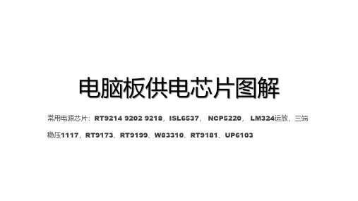
稳压1117,RT9173、RT9199、W83310、RT9181、UP6103•1.三端稳压器117降压1117,3.3代表类型(3.3V输出)ADJ,可调节•开关电源工作原理:PWM 芯片控制 MOS 的高速开关来调节电压,当开关打开时电压上升,而关闭时则电压下降,电感电容组成 LC 储能电路。
通过高速切换 MOS 的开和关,控制 MOS 导通时间来控制电压的准位。
如图 T代表一个周期,T1 为开启状态,T2 为关闭状态,只要控制 T1 和 T2 的时间就可以控制电压的高低。
通过给负载馈电的时间改变供电电压当K闭合,则小灯泡获得12V电压;当K断开,小灯泡获得0V电压。
若K闭合1秒,断开一秒,重复动作1分钟,则在1分钟内小灯泡获得的平均电压:1分钟/(1开+1关)*12V=6.0V。
改变导通和截止的时间比例(占空比)就可以改变小灯泡获得的平均电压。
但这个电压不连续。
为了获得一个持续的电压。
电路加入滤波器件。
通常由窜连电感和并联的滤波电路来实现。
即上管导通下管闭合。
电感及电容端电压不能突变的特性使得上下管的导通给电感及电容提供了源源不断的电压经由电路构成回路,提供稳定的电流。
• 478主板平台内存供电一般比较器+场效应管的方式。
775以上的内存供电采用PWM方式供电。
供电芯片通常有RT9202、RT9214、RT9218等•RT9202引脚定义采用 12V 和 5V 供电的 RT9202 工作流程:1:5V 给 5 脚供电,5V 给上管供电,12V 经过 R4 给 1 脚供电,5V 经过 R1 给 7 脚供电;2:2 脚 UGATE 驱动上管导通;3:上管给电感 L2 和电容 C3 充电;4:当 L2 和 C3 成的储能电路电压经过 R2 和 R3 分压反馈给 FB 脚电压超过 0.8V 时,RT9202 关闭上管打开下管5:下管导通构成储能电路的放电回路,当电路经过分压后反馈给 FB 的电压低于 0.8V 时,RT9202 控制关闭下管打开上管,继续充电;6:2-5 循环。
- 1、下载文档前请自行甄别文档内容的完整性,平台不提供额外的编辑、内容补充、找答案等附加服务。
- 2、"仅部分预览"的文档,不可在线预览部分如存在完整性等问题,可反馈申请退款(可完整预览的文档不适用该条件!)。
- 3、如文档侵犯您的权益,请联系客服反馈,我们会尽快为您处理(人工客服工作时间:9:00-18:30)。
DS9212-05 March 2007Dual 5V Synchronous Buck PWM DC-DC and Linear Power ControllerFeaturesz Operating with Single 5V Supply Voltage z Drives All Low Cost N-MOSFETs z Voltage Mode PWM Controlz 300kHz Fixed Frequency Oscillator zFast Transient Response :Full 0% to 100% Duty Ratio z Internal Soft-Startz Adaptive Non-Overlapping Gate DriverzOver-Current Fault Monitor on V CC , No Current Sense Resistor RequiredzRoHS Compliant and 100% Lead (Pb)-FreeApplicationsz Graph Cardz Motherboard, Desktop Servers z IA Equipmentsz Telecomm EquipmentszHigh Power DC-DC RegulatorsPin ConfigurationsOrdering InformationGeneral DescriptionThe RT9212 is a 3-in-one power controller delivers high efficiency and tight regulation from two voltage regulating synchronous buck PWM DC-DC and one linear power controllers.The RT9212 can control two independent output voltages adjustment in range of 0.8V to 4.0V with 180 degrees channel to channel phase operation to reduce input ripple.In dual power supply application the RT9212 monitors the output voltage of both Channel 1 and Channel 2. An independent PGOOD (power good) signal is asserted for each channel after the soft-start sequence has completed,and the output voltage is within ±15% of the set point. The linear controller drives an external transistor to provide an adjustable output voltage.Built-in over-voltage protection prevents the output from going above 137.5% of the set point by holding the lower MOSFET on and the upper MOSFET off. Adjustable over-current protection (OCP) monitors the voltage drop across the R DS(ON) of the upper MOSFET for each synchronous buck PWM DC-DC controller individually.(TOP VIEW)UGATE1BOOT1PHASE1NC OCSET2/SD OCSET1/SD PVCC1PGND1FB1COMP1FB2PGOOD NC LGATE1FBL NC GNDA VCC DRVPHASE2BOOT2PGND2LGATE2UGATE2TSSOP-24Note :RichTek Pb-free and Green products are :`RoHS compliant and compatible with the current require- ments of IPC/JEDEC J-STD-020.`Suitable for use in SnPb or Pb-free soldering processes.`100% matte tin (Sn) plating.RT9212P : Pb Free with Commercial Standard G : Green (Halogen Free with Commer- cial Standard)Typical Application Circuit1.8V1.5VOUT1OUT2V OUT1 & V OUT2 )DS9212-05 March 2007Functional Pin DescriptionUGATE1 (Pin 1)Channel 1 upper gate driver output. Connect to gate of the high-side power N-MOSFET . This pin is monitored by the adaptive shoot-through protection circuitry to determine when the upper MOSFET has turned off.BOOT1 (Pin 2)Bootstrap supply pin for the upper gate driver. Connect the bootstrap capacitor between BOOT1 pin and the PHASE1 pin. The bootstrap capacitor provides the charge to turn on the upper MOSFET .PHASE1 (Pin 3)Connect this pin to the source of the upper MOSFET and the drain of the lower MOSFET. PHASE1 is used to monitor the Voltage drop across the upper MOSFET of the channel 1 regulator for over-current protection.NC (Pin 4, 7, 8)No connection. Don ’t connect any component to this pin.FB1 (Pin 5)Channel 1 feedback voltage. This pin is the inverting input of the error amplifier. FB1 senses the channel 1 through an external resistor divider P1 (Pin 6)Channel 1 external compensation. This pin internally connects to the output of the error amplifier and input of the PWM comparator. Use a RC + C network at this pin to compensate the feedback loop to provide optimum transient response.GNDA (Pin 9)Signal ground for the IC. All voltage levels are measured with respect to this pin. Ties the pin directly to ground plane with the lowest impedance.PHASE2 (Pin 10)Connect this pin to the source of the upper MOSFET and the drain of the lower MOSFET. PHASE2 is used to monitor the Voltage drop across the upper MOSFET of the channel 2 regulator for over-current protection.BOOT2 (Pin 11)Bootstrap supply pin for the upper gate driver. Connect the bootstrap capacitor between BOOT2 pin and the PHASE2pin. The bootstrap capacitor provides the charge to turn on the upper MOSFET .UGATE2 (Pin 12)Channel 2 upper gate driver output. Connect to gate of the high-side power N-MOSFET . This pin is monitored by the adaptive shoot-through protection circuitry to determine when the upper MOSFET has turned off.PGND2 (Pin 13)Return pin for high currents flowing in low-side power N-MOSFET . Ties the pin directly to the low-side MOSFET source and ground plane with the lowest impedance.LGATE2 (Pin 14)Channel 2 lower gate drive output. Connect to gate of the low-side power N-MOSFET . This pin is monitored by the adaptive shoot-through protection circuitry to determine when the lower MOSFET has turned off.VCC (Pin 15)Connect this pin to a well-decoupled 5V bias supply. It is also the positive supply for the lower gate driver, LGATE2.DRV (Pin 16)Connect this pin to the base of an external transistor. This pin provides the drive for the linear regulator's pass transistor.FBL (Pin 17)Linear regulator feedback voltage. This pin is the inverting input of the error amplifier and protection monitor. Connect this pin to the external resistor divider network of the linear regulator.FB2 (Pin 18)Channel 2 feedback voltage. This pin is the inverting input of the error amplifier. FB2 senses the channel 2 through an external resistor divider network.Function Block DiagramMOSFETupper the of R 40uA I DS(ON)OCSETOCSET R ×=GNDAPGOOD (Pin 19)PGOOD is an open-drain output used to indicate that both the channel 1 and channel 2 regulators are within normal operating voltage ranges.OCSET2/SD (Pin 20), OCSET1/SD (Pin 21)Connect a resistor (R OCSET ) from this pin to the drain of the upper MOSFET of the supply voltage sets the over-current trip point. R OCSET , an internal 40μA current source , and the upper MOSFET on-resistance, (R DS(ON), set the converter over-current trip point (I OCSET ) according to the following equation:An over-current trip cycles the soft-start function. Pulling the pin to ground resets the device and all external MOSFETs are turned off allowing the two output voltage power rails to float.PVCC1 (Pin 22)Connect this pin to a well-decoupled 5V supply. It is also the positive supply for the lower gate driver, LGATE1.LGATE1 (Pin 23)Channel 1 power gate drive output. Connect to gate of the low-side power N-Channel MOSFET . This pin is monitored by the adaptive shoot-through protection circuitry to determine when the lower MOSFET has turned off.PGND1 (Pin 24)Return pin for high currents flowing in low-side power N-MOSFET . Ties the pin directly to the low-side MOSFET source and ground plane with the lowest impedance.DS9212-05 March 2007Electrical Characteristics(V= 5V, T = 25°C, unless otherwise specified)To be continuedRecommended Operating Conditions (Note 3)z Supply Voltage, V CC -------------------------------------------------------------------------------------------------5V ± 5 %z Ambient T emperature Range ---------------------------------------------------------------------------------------0°C to 70°C zJunction T emperature Range ---------------------------------------------------------------------------------------0°C to 125°CAbsolute Maximum Ratings (Note 1)z Supply Voltage, V CC -------------------------------------------------------------------------------------------------7V z BOOT , V BOOT - V PHASE -----------------------------------------------------------------------------------------------7Vz Input, Output or I/O Voltage ----------------------------------------------------------------------------------------GND-0.3V to 7V zPackage Thermal ResistanceTSSOP-24, θJA --------------------------------------------------------------------------------------------------------100°C/W z Junction T emperature ------------------------------------------------------------------------------------------------150°C z Lead Temperature (Soldering, 10 sec.)--------------------------------------------------------------------------260°Cz Storage T emperature Range ---------------------------------------------------------------------------------------−65°C to 150°C zESD Susceptibility (Note 2)HBM (Human Body Mode)-----------------------------------------------------------------------------------------2kV MM (Machine Mode)-------------------------------------------------------------------------------------------------200VNote 1.Stresses listed as the above“Absolute Maximum Ratings”may cause permanent damage to the device. These are for stress ratings. Functional operation of the device at these or any other conditions beyond those indicated in the operational sections of the specifications is not implied. Exposure to absolute maximum rating conditions forextended periods may remain possibility to affect device reliability.Note 2. Devices are ESD sensitive. Handling precaution recommended.Note 3. The device is not guaranteed to function outside its operating conditions.DS9212-05 March 2007Typical Operating CharacteristicsPower Good RisingV OUT2(2V/Div)PGOOD (5V/Div)Time (5ms/Div)V OUT1(2V/Div)V CC (5V/Div)UGATE Phase Shift UGATE2(5V/Div)Time (1us/Div)UGATE1(5V/Div)LGATE Phase ShiftLGATE2(5V/Div)Time (1us/Div)LGATE1(5V/Div)Power OnV OUT1(2V/Div)V OUT2(2V/Div)UGATE2(5V/Div)Time (5ms/Div)UGATE1(10V/Div)I OUT1 = I OUT2 = 5APower OffV OUT1(2/Div)V OUT2(2/Div)UGATE2(5V/Div)Time (500us/Div)UGATE1(10/Div)I OUT1 = I OUT2 = 5APower Good FallingV CC (5V/Div)Time (25ms/Div)V OUT1(2V/Div)V OUT2(2V/Div)PGOOD (5V/Div)V OUT2 TransientTime (250us/Div)V OUT2(10mV/Div)I OUT2(5A/Div)V OUT1 Transient Time (250us/Div)V OUT1(100mV/Div)I OUT1(5A/Div)BootstrapLGATE1(5V/Div)Time (1us/Div)UGATE1(5V/Div)BootstrapLGATE2(5V/Div)Time (1us/Div)UGATE2(5V/Div)V OUT2 ShortTime (5ms/Div)V OUT2(1V/Div)UGATE2(10V/Div)LGATE2(5V/Div)V OUT1 Short LGATE1(5V/Div)Time (5ms/Div)UGATE1(10V/Div)V OUT1(2V/Div) V IN = 5V, V OUT = 3.3V, C OUT = 3000μFV IN = 5V, V OUT = 2.5V, C OUT = 3000μFDS9212-05 March 2007Iocset & Temperature303540455055-40-2020406080100120140Temperature Io c s e t (μA )(°C)Reference vs. Temperature0.7880.790.7920.7940.7960.7980.80.8020.8040.8060.808-40-2020406080100120Temperature F Bv o l t a g e (V )(°C)POR (Start Up)V OUT1(2V/Div)V OUT2(2V/Div)V CC (5V/Div)Time (5ms/Div)V OUT3(200mV/Div)V OUT3 TransientTime (2.5ms/Div)I OUT3(2A/Div)V IN = 5V, V OUT= 1.8VFrequency vs. Temperature285290295300305310315-40-20020406080100120Temperature F r e q u e n c y (k H z ) (°C)POR (Rising/Falling) vs. Temperature3.93.9544.054.14.154.24.25-40-10205080110140Temperature P O R (V )(°C)Applications InformationInductorThe inductor is required to supply constant current to the output load. The inductor is selected to meet the output voltage ripple requirements and minimize the converter's response time to the load transient.A larger value of inductance reduces ripple current and voltage. However, the larger value of inductance has a larger physical size, lower output capacitor and slower transient response time.A good rule for determining the inductance is to allow the peak-to-peak ripple current in the inductor to be approximately 30% of the maximum output current. The inductance value can be calculated by the following equation :WhereV IN is the input voltage,V OUT is the output voltage,F S is the switching frequency,IOUT is the peak-to-peak inductor ripple current.The inductance value determines the converter's ripple current and the ripple voltage. The ripple current is calculated by the following equations :Increasing the value of inductance reduces the ripple current and voltage. However, the large inductance values raise the converter's response time to a load transient.One of the parameters limiting the converter's response to a load transient is the time required to change the inductor current. Given a sufficiently fast control loop design, the RT9212 will provide 0% to 100% duty cycle in response to a load transient.The response time is the time required to slew the inductor current from an initial current value to the transient current level. The inductor limit input current slew rate during the load transient. Minimizing the transient response time can minimize the output capacitance required. The response time is different for application of load and removal of load to a transient. The following equations give the approximate response time for application and removal of a transient load :WhereT Rise is the response time to the application of load,T Fall is the response time to the removal of load,IOUT is the transient load current step.Input CapacitorThe input capacitor is required to supply the AC current to the Buck converter while maintaining the DC input voltage.The capacitor should be chosen to provide acceptable ripple on the input supply lines. Use a mix of input bypass capacitors to control the voltage overshoot across the MOSFET s. Use small ceramic capacitors for high frequency decoupling and bulk capacitors to supply the current. Place the small ceramic capacitors close to the MOSFETs and between the drain of Q1/Q3 and the source of Q2/Q4.The key specifications for input capacitor are the voltage rating and the RMS current rating. For reliable operation,select the bulk capacitor with voltage and current ratings above the maximum input voltage and largest RMS current.The capacitor voltage rating should be at least 1.25 times greater than the maximum input voltage and voltage rating of 1.5 times is a conservative guideline. The RMS current rating for the input capacitor of a buck regulator should be greater than approximately 0.5 the DC load current.−×=××IN OUT OUTIN (V V )V ΔI V Fs LOUTIN OUT Rise V V ΔI L T −×=OUTOUT Fall V ΔI L T ×=−×=××IN OUT OUT IN S OUT(V V )V L V F ΔI ΔΔ,DS9212-05 March 2007Output CapacitorThe output capacitor is required to maintain the DC output voltage and supply the load transient current. The capacitor must be selected and placed carefully to yield optimal results and should be chosen to provide acceptable ripple on the output voltage.The key specification for output capacitor is its ESR. Low ESR capacitors are preferred to keep the output voltage ripple low. The bulk capacitor's ESR will determine the output ripple voltage and the initial voltage drop after a high slew-rate transient. For transient response, a combination of low value, high frequency and bulk capacitors placed close to the load will be required. High frequency decoupling capacitors should be placed as close to the power pins of the load as possible. In most cases, multiple electrolytic capacitors of small case size perform better than a single large case capacitor.The capacitor value must be high enough to absorb the inductor's ripple current. The output ripple is calculated as :Another concern is high ESR induced output voltage ripple may trigger UV or OV protections will cause IC shutdown.MOSFETThe MOSFET should be selected to meet power transfer requirements is based on maximum drain-source voltage (V DS ), gate-source drive voltage (V GS ), maximum output current, minimum on-resistance (R DS(ON)) and thermal management.In high-current applications, the MOSFET power dissipation, package selection and heatsink are the dominant design factors. The losses can be divided into conduction and switching losses.Conduction losses are related to the on resistance of MOSFET , and increase with the load current. Switching losses occur on each ON/OFF transition. The conduction losses are the largest component of power dissipation for both the upper and the lower MOSFETs.For the Buck converter the average inductor current is equal to the output load current. The conduction loss is defined as :P CD (high side switch) = I O 2 * R DS(ON) * D P CD (low side switch) = I O 2 * R DS(ON) * (1-D)The switching loss is more difficult to calculate. The reason is the effect of the parasitic components and switching times during the switching procedures such as turn-on /turn-off delays and rise and fall times. With a linear approximation, the switching loss can be expressed as :P SW = 0.5 * V DS(OFF) * I O * (T Rise + T Fall ) * F WhereV DS(OFF) is drain to source voltage at off time,T Rise is rise time,T Fall is fall time,F is switching frequency.The total power dissipation in the switching MOSFET can be calculate as :P High Side Switch =I O 2 * R DS(ON)* D + 0.5 * V DS(OFF)* I O * (T Rise + T Fall )* F P Low Side Switch = I O 2 * R DS(ON) * (1-D)For input voltages of 3.3V and 5V, conduction losses often dominate switching losses. Therefore, lowering the R DS(ON)of the MOSFETs always improves efficiency.Feedback CompensationThe RT9212 is a voltage mode controller; the control loop is a single voltage feedback path including an error amplifier and PWM comparator as Figure 1 shows. In order to achieve fast transient response and accurate output regulation, a adequate compensator design is necessary. The goal of the compensation network is to provide adequate phase margin (greater than 45 degrees) and the highest 0dB crossing frequency. And to manipulate loop frequency response that its gain crosses over 0dB at a slope of -20dB/dec.ESR I V OUT OUT ×Δ=ΔModulator Frequency EquationsThe modulator transfer function is the small-signal transfer function of V OUT /V E/A . This transfer function is dominated by a DC gain and the output filter (L O and C O ), with a double pole frequency at F LC and a zero at F ESR . The DC gain of the modulator is the input voltage (V IN ) divided by the peak-to-peak oscillator voltage V RAMP .The first step is to calculate the complex conjugate poles contributed by the LC output filter.The output LC filter introduces a double pole,−40dB/decade gain slope above its corner resonant frequency, and a total phase lag of 180 degrees. The Resonant frequency of the LC filter expressed as follows :The next step of compensation design is to calculate the ESR zero. The ESR zero is contributed by the ESR associated with the output capacitance. Note that this requires that the output capacitor should have enough ESR to satisfy stability requirements. The ESR zero of the output capacitor expressed as follows :OO P(LC)C L 21F ××=πESRC 21F O Z(ESR)××=π)C // (C R 21F C R 21F 0F 2 1 2P122Z1P1×=××==ππFigure 2Figure 3 shows the DC-DC converter's gain vs. frequency.The compensation gain uses external impedance networks Z C and Z F to provide a stable, high bandwidth loop.High crossover frequency is desirable for fast transient response, but often jeopardize the system stability. In order to cancel one of the LC filter poles, place the zero before the LC filter resonant frequency. In the experience, place the zero at 75% LC filter resonant frequency.Crossover frequency should be higher than the ESR zero but less than 1/5 of the switching frequency.The second pole be place at half the switching frequency.PWM Figure 1Compensation Frequency EquationsThe compensation network consists of the error amplifier and the impedance networks Z C and Z F as Figure 2 shows.Figure 3DS9212-05 March 2007Layout ConsiderationThe layout is very important when designing high frequency switching converters. Layout will affect noise pickup and can cause a good design to perform with less than expected results.1. Even though double-sided PCB is usually sufficient for a good layout, four-layer PCB is the optimum approach to reducing the noise. Use the two internal layers as the power and GND planes, the top layer for power connections with wide, copper filled areas, and the bottom layer for the noise sensitive traces.2. There are two sets of critical components in a DC-DC converter. The switching components are the most critical because they switch large amounts of energy, and therefore tend to generate large amounts of noise. The others are the small signal components that connect to sensitive nodes or supply critical bypass current and signal coupling.Make all critical component ground connections with vias to GND plane.3. Use fewer, but larger output capacitors, keep the capacitors clustered, and use multiple layer traces with heavy copper to keep the parasitic resistance low. Place the output capacitors as close to the load as possible.4. The inductor, output capacitor and the MOSFET should be as close to each other as possible. This helps to reduce the EMI radiated.5. Place the switching MOSFET as close to the input capacitors as possible. The MOSFET gate traces to the IC must be as short, straight, and wide as possible. Use copper filled polygons on the top and bottom layers for the PHASE nodes.6. Place the C BOOT as close as possible to the BOOT and PHASE pins.7. The feedback part of the system should be kept away from the inductor and other noise sources, and be placed close to the IC. Connect to the GND pin with a single trace, and connect this local GND trace to the output capacitor GND.8. Minimize the leakage current paths on the OCSET/SD pin and locate the resistor as close to the OCSET/SD pin as possible because the internal current source is only 40μA.9. In multilayer PCB, use one layer as ground plane and have a control circuit ground (analog ground), to which all signals are referenced. The goal is to localize the high current path to a separate loop that does not interfere with the more sensitive analog control function. These two grounds must be connected together on the PC board layout at a single point.Reference VoltageBecause one of the RT9212 regulators uses a low 35dB gain error amplifier, shown in Figure 4. The voltage regulation is dependent on V IN & V OUT setting.The FB reference voltage of 0.8V is trimmed at V IN = 5V &V OUT = 2.5V condition. In a fixed V IN = 5V application, the FB reference voltage vs. V OUT voltage can be calculated as Figure 5.Figure 4Figure 50.7750.780.7850.790.7950.80.8050.810.81511.522.533.544.55V OUT (V)F B (V )FB1.9VR2Richtek Technology Corporation Headquarter5F, No. 20, Taiyuen Street, Chupei City Hsinchu, Taiwan, R.O.C.Tel: (8863)5526789 Fax: (8863)5526611Richtek Technology Corporation Taipei Office (Marketing)8F, No. 137, Lane 235, Paochiao Road, Hsintien City Taipei County, Taiwan, R.O.C.Tel: (8862)89191466 Fax: (8862)89191465Email: marketing@L24-Lead TSSOP Plastic Package Outline Dimension。