SpiraClock A Continuous and Non-Intrusive Display for Upcoming Events
莱埃尔电子有限公司产品说明:拉瓦雷特时间间隔计数器说明书

LAUREL ELECTRONICS, INC.Laureate™ Time Interval Meter Resolution to 0.2 µs for time of periodic events. Displays highly accurate rate based on 1 / time.Features•Times periodic events with width from 1 µs to 199.999 s•Display resolution to 0.2 µs•Rep rates to 250 kHz•Inputs from NPN or PNP proximity switches, contact closures, digital logic,magnetic pickups down to 12 mV, or AC inputs up to 250 Vac•Triggers on positive or negative pulse edges•Universal AC power, 85-264 Vac•Isolated 5, 10 or 24 Vdc excitation supply to power sensors•NEMA 4X, 1/8 DIN case•Optional serial I/O: Ethernet, USB, RS232, RS485, Ethernet-to-RS485 converter•Optional relay outputs: dual or quad relays, contact or solid state•Optional isolated analog output: 4-20 mA, 0-20 mA, 0-10V, -10 to +10V•Optional low voltage power: 10-48 Vdc or 12-32 Vac•Optional Extended Timer: features of standard timer plus rate based on 1/time DescriptionThe Laureate A-to-B Time Interval Meter can display pulsewidth or time delay between individual pulses to a resolution of0.2 µs. It can also display average pulse width or average timedelay between multiple pulses.Time interval is measured between inputs on channels A andB. Timing starts when a pulse is applied to Channel A (selectablepositive or negative edge), and ends when a pulse is applied toChannel B (selectable positive or negative edge). In case of asingle pulsed signal, the A and B inputs can be tied together. Apositive or negative slope may be selected to start timing, andthe opposite slope must be selected to stop timing. Timing isachieved by counting 5.5 MHz clock pulses. Multiple integral timeintervals are averaged over a gate time which is selectable from10 ms to 199.99 s and also controls the display update time.Time interval can be displayed in seconds, milliseconds, ormicroseconds with 6-digit resolution. In the typical application,time is displayed in milliseconds with 1 µs resolution. For timesless than 100 ms, display resolution down to 0.2 µs can beachieved by applying a multiplier of 10, moving the decimal pointby one position, and averaging many time intervals.Highly accurate rate can be displayed by taking the inverse oftime. Extensive arithmetic capabilities allow display inengineering units, such as meters/sec. Rate based on timerequires use of the Extended counter main board.The FR dual-channel signal conditioner board accepts inputsfrom proximity switches with PNP or NPN output, TTL or CMOSlogic, magnetic pickups, contact closures, and other signals from12 mV to 250 Vac. Jumper selections provide optimum operationfor different sensor types and noise conditions. A built-in isolated5, 10, or 24 Vdc excitation supply can power proximity switchesand other sensors, and eliminate the need for an external powersupply.Designed for system use. Optional plug-in boards includeEthernet and other serial communication boards, dual or quadrelay boards, and an isolated analog output board. Laureatesmay be powered from 85-264 Vac or optionally from 12-32 Vacor 10-48 Vdc. The display is available with red or green LEDs.The 1/8 DIN case meets NEMA 4X (IP65) specifications from thefront when panel mounted. Any setup functions and front panelkeys can be locked out for simplified usage and security. A built-in isolated 5, 10, or 24 Vdc excitation supply can power trans-ducers and eliminate the need for an external power supply.All power and signal connections are via UL / VDE / CSA ratedscrew clamp plugs.SpecificationsDisplayReadoutRangeIndicators6 LED digits, 7-segment, 14.2 mm (.56"), red or green-999999 to +999999Four LED lampsInputsTypes Grounding Minimum Signal Maximum Signal Noise Filter Contact Debounce AC, pulses from NPN, PNP transistors, contact closures, magnetic pickups. Common ground for channels A & BNine ranges from (-12 to +12 mV) to (+1.25 to +2.1V).250 Vac1 MHz, 30 kHz, 250 Hz (selectable)0, 3, 50 ms (selectable)Time Interval ModeTiming StartTiming StopPeriodic Timing Interval Gate TimeTime Before Zero Output Channel A pulse, + or - edges Channel B pulse, + or - edgesGate time + 30 ms + 0-2 time intervals Selectable 10 ms to 199.99 s Selectable 10 ms to 199.99 sResolution0 - 199.999 s 0 - 99.9999 s 0 - 9.99999 s 0 - .999999 s 0 - .099999 s 1 ms 100µs 10 µs 1 µs 0.2 µsAccuracyTime Base Span Tempco Long-term Drift Crystal calibrated to ±2 ppm ±1 ppm/°C (typ)±5 ppm/yearPowerVoltage, standard Voltage, optional Power frequency Power consumption (typical, base meter) Power isolation 85-264 Vac or 90-300 Vdc12-32 Vac or 10-48 VdcDC or 47-63 Hz1.2W @ 120 Vac, 1.5W @ 240 Vac, 1.3W @ 10 Vdc, 1.4W @ 20 Vdc, 1.55W @ 30 Vdc, 1.8W @ 40 Vdc,2.15W @ 48 Vdc250V rms working, 2.3 kV rms per 1 min testExcitation Output (standard)5 Vdc10 Vdc24 VdcOutput Isolation 5 Vdc ± 5%, 100 mA 10 Vdc ± 5%, 120 mA 24 Vdc ± 5%, 50 mA 50 Vdc to meter groundAnalog Output (optional)Output Levels Current compliance Voltage compliance Scaling Resolution Isolation 4-20 mA, 0-20 mA, 0-10V, -10 to +10V (single-output option) 4-20 mA, 0-20 mA, 0-10V (dual-output option)2 mA at 10V ( > 5 kΩ load)12V at 20 mA ( < 600Ω load)Zero and full scale adjustable from -99999 to +9999916 bits (0.0015% of full scale)250V rms working, 2.3 kV rms per 1 min test(dual analog outputs share the same ground)Relay Outputs (optional)Relay Types Current Ratings Output common Isolation 2 Form C contact relays or 4 Form A contact relays (NO)2 or 4 Form A, AC/DC solid state relays (NO)8A at 250 Vac or 24 Vdc for contact relays120 mA at 140 Vac or 180 Vdc for solid state relays Isolated commons for dual relays or each pair of quad relays 250V rms working, 2.3 kV rms per 1 min testSerial Data I/O (optional)Board SelectionsProtocols Data RatesDigital Addresses Isolation Ethernet, Ethernet-to-RS485 server, USB, USB-to-RS485 server, RS485 (dual RJ11), RS485 Modbus (dual RJ45), RS232 Modbus RTU, Modbus ASCII, Laurel ASCII protocol 300 to 19200 baud247 (Modbus), 31 (Laurel ASCII),250V rms working, 2.3 kV rms per 1 min testEnvironmental Operating Temperature Storage Temperature Relative Humidity Protection0°C to 55°C -40°C to 85°C95% at 40°C, non-condensingNEMA-4X (IP-65) when panel mountedElectrical ConnectionsMechanicalApplication ExamplesTime Interval Mode for Time DelayFor periodic pulses applied to A and B channels, time delays can be measured down to 0.2 µs resolution from the rising or falling edge of A to the rising or falling edge of B (selectable). Time Interval Mode for Pulse WidthThe width of periodic pulses (t1 or t2) can be measured by tying the A and B channels together. As for time delay, readings are averaged over a user-selectable gate time. Timing Process DynamicsThe start and stop pulses used for timing can be generated by the dual relay board in a Laureate panel meter or digital counter. For instance, the start and stop pulse edges can be created as temperature passes two alarm setpoints, or temperature cycles in a hysteresis control mode. Rate Based on 1 / TimeThe start and stop pulses used for timing can be generated by the dual relay board in a Laureate panel meter or digital counter. For instance, the start and stop pulse edges can be created as temperature passes two alarm setpoints, or temperature cycles in a hysteresis control mode.Replacing an Oscilloscope with a Laureate Time Interval MeterAn oscilloscope is great for viewing and timing pulses in a lab. However, in fixed installations where digital timing accuracy and control outputs are required, a low-cost Laureate time interval meter will be the instrument of choice. Resolution to 0.2 µs is feasible.Instrumenting a Pulsed Laser SystemSome of the many possibilities in instrumenting a pulsed laser system with Laureate dual-channelcounters: elapsed time, number of pulses, pulse width, pulse separation, duty cycle, and pulse rep rate.Ordering GuideCreate a model number in this format: L50000FR, IPCMain Board L5 Standard Main Board, Green LEDsL6 Standard Main Board, Red LEDsL7 Extended Main Board, Green LEDsL8 Extended Main Board, Red LEDsNote: Use of the Extended Main Board makes this counter also suitable for A-B time interval,frequency, rate, period, square root of rate, up or down total, arithmetic functions, simultaneousrate and total, phase, duty cycle, batching, and custom curve linearization.Power0 Isolated 85-264 Vac1 Isolated 12-32 Vac or 10-48 VdcRelay Output (isolated) 0 None1 Two 8A Contact Relays2 Two 120 mA Solid State Relays3 Four 8A Contact Relays4 Four 120 mA Solid State RelaysAnalog Output (isolated) 0 None1 Single isolated 4-20 mA, 0-20 mA, 0-10V, -10 to +10V2 Dual isolated 4-20 mA, 0-20 mA, 0-10VDigital Interface (isolated) 0 None1 RS2322 RS485 (dual RJ11 connectors)4 RS485 Modbus (dual RJ45 connectors)5 USB6 USB-to-RS485 converter7 Ethernet8 Ethernet-to-RS485 converterInput Type FR Dual-Channel Pulse Input Signal ConditionerAdd-on Options CBL01RJ11-to-DB9 cable. RJ11 to DB9. Connects RS232 ports of meter and PC.CBL02USB-to-DB9 adapter cable. Combination of CBL02 and CBL01 connects meter RS232port to PC USB port.CBL03-16-wire data cable, RJ11 to RJ11, 1 ft. Used to daisy chain meters via RS485.CBL03-76-wire data cable, RJ11 to RJ11, 7 ft. Used to daisy chain meters via RS485.CBL05USB cable, A-B. Connects USB ports of meter and PC.CBL06USB to RS485 adapter cable, half duplex, RJ11 to USB. Connects meter RS485 portto PC USB port.CASE1Benchtop laboratory case for one 1/8 DIN meterCASE2Benchtop laboratory case for two 1/8 DIN metersIPC Splash-proof coverBOX1NEMA-4 EnclosureBOX2NEMA-4 enclosure plus IPCBL Blank Lens without button padsNL Meter lens without button pads or Laurel logo。
Clock Network Sizing in Presence of Power Supply Noise
Clock Network Sizing in Presence of Power Supply Noise Kai Wang and Malgorzata Marek-SadowskaDepartment of Electrical and Computer EngineeringUniversity of California,Santa BarbaraIBM Technical Contact–Sani NassifManager,Tools and Technology,Austin Research LaboratoryAbstractIn this paper,we present a novel sequential linear programming approach to the problem of clock network sizing.The original nonlinear programming problem is transformed to a sequence of linear programs,by taking thefirst order Taylor’s expansion of clock path delay with respect to buffer and wire widths.The sensitivities of clock path delay,with respect to buffer and wire widths,are effi-ciently updated for each linear program by applying time domain analysis to the clock network in a divide-and-conquer fashion.Our technique takes into account pro-cess variation and power supply noise,which have signif-icant impacts on clock skew.We demonstrate experimen-tally that the proposed technique is not only capable of ef-fectively optimizing clock skew and power consumption, but also able to provide more accurate delay and skew re-sults compared to the traditional approach.1.IntroductionIn a synchronous digital design,the most common strategy for clock distribution is to insert a large num-ber of buffers along the paths from clock source to sinks,forming a buffered tree structure.Carrying large loads and switching at the highest frequency,clock is one of the major sources of power dissipation in a dig-ital integrated circuit.Reducing clock power dissipa-tion is an effective technique for low-power designs. The clock skew,defined as the maximum difference be-tween the arrival times of the signals at all the clock sinks,significantly impacts the performance of the sys-tem.Clock power and skew optimization have become the dominant objectives in clock design.Traditional works in clock network design achieve zero or bounded skew,by adjusting either the wire lengths([18],[5])or the wire/buffer widths([23]).Some other works focus on clock skew scheduling,which de-termines the intensional skews for clock sinks to im-prove the system performance or reliability.Existing clock skew scheduling techniques([8],[16],[19])gen-erate a clock schedule without considering its impact on the layout of clock network,thus the resulting clock network based on the pre-defined skew may not achieve an optimal solution in terms of area or power.Recently, the UST-BP algorithm in[22]and the UST/DME al-gorithm in[17]have incorporated simultaneous skew scheduling and clock routing.The authors consider the routing problem of useful skew tree(UST)under gen-eral clock skew constraints.However,clock buffers are not considered in their formulations.Power supply variation is one of the main causes of the clock skew.Because of the resistive nature of power grid wires and inductive parasitics,power sup-ply variation(noise)occurs when large currents are delivered during logic transitions.Power supply noise causes a drastic degradation of system performance,or may even cause a chip failure.Specifically,clock tim-ing characteristics such as delay and skew are signifi-cantly impacted by the power supply noise because the clock network spans the entire chip and comprises a large number of buffers.Ironically,clock switching it-self is one of the most serious sources of power sup-ply noise because clock buffers draw a large portion of current with the highest frequency.A clock distribu-tion network designed without considering delay vari-ations induced by power supply noise may suffer sig-nificant degradations of its skew during the chip oper-ation.The existing clock synthesis techniques don’t con-sider power supply noise because they are usually ap-plied at the early design stages,when the detailed lay-out and switching current information are not yet avail-able.It is difficult to estimate the power supply vari-ation and apply it in the process of clock skew min-imization.However,at the later design stages,when the placement of logic blocks,global routing,and pre-synthesis of clock tree have beenfinished,the power supply variations can be more accurately estimated by simulating the full chip,including power distribution network,pre-synthesized clock network,and other logic blocks.At this point,we are in a position to address the impact of power supply noise on clock timing.The problem of clock skew verification in the presence of power supply noise has been studied in[15].As technol-ogy scales,power supply network is expected to experi-ence increasingly greater noise due to higher frequency and higher degree of integration.Thus the impact of power supply noise on clock networks will become in-creasingly severe and must be considered in clock net-work synthesis.The majority of the existing methods of clock de-sign are based on analytical delay models,such as Elmore delay[7]for interconnects,and simple RC model[20]for buffers.As the process technology scales down,many physical effects previously considered to be second-order,now are becoming prominent.Those effects may not be accurately captured by the analyti-cal delay models.It is worth noting that the accuracy required to calculate delay differences is much greater than the accuracy required to calculate the absolute de-lay values[9].Hence clock skew optimization that de-pends only on analytical delay models may not be suf-ficiently accurate for skew control.Clock buffer sizing is an effective technique for skew control and power minimization.The problem of low-power clock buffer sizing for the bounded-skew con-straint has been studied in[21].In practice,general skew constraints introduce substantialflexibility in op-timizing clock performance and power dissipation.In this paper,we consider the problem of buffer siz-ing for clock power minimization,subject to general skew constraints.We propose a novel approach based on sequential linear programming(SLP).We transform the constrained nonlinear programming problem into a sequence of linear programs,by taking thefirst-order Taylor’s expansion of clock path delay with respect to buffer widths.Instead of relying on any analytical de-lay model,our technique applies time-domain analy-sis to the clock network to compute the sensitivities of clock path delay with respect to buffer widths.This calculation is efficient because we adopt a divide-and-conquer algorithm,which has a linear complexity with respect to the number of clock buffers.Our technique incorporates clock skew scheduling and buffer sizing,such that the resulting skew sched-ule is not only feasible,but is also optimal for clock power minimization.We compute accurate skew and delay because our technique applies time-domain anal-ysis.We can also take into account the impact of pro-cess variations and power supply noise.The rest of the paper is organized as follows.Sec-tion2describes the problem formulation.In section3 we discuss the sequential linear programming ap-proach.The sensitivity calculation algorithm is pre-sented in section4.In section5we show how to extend our technique to consider the impact of power sup-ply noise.The experimental results are shown in sec-tion6.We discuss our future work in section7and conclude the paper in section8.2.Problem FormulationTo facilitate our discussion,we introduce the fol-lowing notations.Let T be the given initial buffered clock tree with M clock sinks and K clock buffers.For each clock buffer b k(k=1,...,K),w k is its width and w tk,w bkare the upper and lower bounds,respectively. We use p(b k)to denote b k’s direct parent buffer,C(b k) to denote the set of b k’s direct child buffers.slew(b k) denotes the slew rate of the clock signal at the b k’s input node,and F C(b k)denotes the set of the clock sinks that are in b k’s fan-out cone.For each clock sink s j(j=1,...,M),d j is the delay from the clock tree root to s j.For a sink s j∈F C(b k),we use b(k,j)to de-note the b k’s direct child buffer that is on the path from b k to s j,and d s(b k,s j)to denote the delay from the b k’s input node to s j.Finally,d r(b k)denotes the delay from clock tree root to the b k’s input node,and d b(b k,b j)de-notes the delay from the input node of buffer b k to the input node of another buffer b j if there is a path from b k to b j.Consider a synchronous circuit with positive edge-triggeredflip-flops in a single-phase clocking scheme. Let F F i and F F j be two sequentially adjacentflip-flops,with F F i feeding data to F F j.We use t i and t j to denote the signal arrival time at the clock pins of F F i and F F j respectively.To ensure correct logic oper-ations,we must bound the skew between F F i and F F j from above and below by the following local skew con-straints:t i−t j≥t maxhold−d minpF F−d minlogic(1)t i−t j≤C P−d maxpF F−d maxlogic−t maxsetup(2)where d minlogicand d maxlogicare the minimum and maximumdelays through the combinational logic;d minpF Fand d maxpF F are the minimum and maximum delay through theflip-flop;t maxholdand t maxsetupare the maximum hold and setup time forflip-flop;and C P is the clock period.In gen-eral,we use SC={t i−t j∈[l i,j,u i,j]}to representthe set of skew constraints for all sequentially adja-cent clock sinks,which must be satisfied by any clock skew schedule.The problem of buffer sizing for clock power min-imization,subject to general skew constraints,is for-mulated as follows.Given an initial buffered clock tree T and a set of skew constraints SC,decide the buffer widths such that the total clock power dissipation is minimized,MinKk=1φk w k(3)subject to skew,buffer width and delay constraints.φk is the constant decided by technology.We discuss the constraints below.1)General skew constraints:For a pair of sequentially adjacent clock sinks s i and s jl i,j≤d i−d j≤u i,j[l i,j,u i,j]∈SC(4) To consider process variation,we assume some un-certainty in the clock delays.There are two constants, 0<α≤1≤β,having the property that if the nominal clock delay is d j,the actual clock delay d j must always fall in the interval[αd j,βd j].For mature process tech-nology,the values ofαandβcan be estimated from previous statistical data.Therefore,considering pro-cess variation,the skew constraint Eqn.(4)is replaced by:βd i−αd j≤u i,j(5)αd i−βd j≥l i,j[l i,j,u i,j]∈SC(6)2)Buffers width bound constraints:w b k≤w k≤w t k k=1,...,K(7)3)Maximal delay constraint:d j≤D max j=1,...,M(8)where D max is the maximal delay specified by the de-signer.The above formulation and the proposed technique can also be extended to handle the skew minimization and bounded-skew optimization problem.Specifically, the general skew constraints are replaced byd f≤d j≤d s j=1,...,M(9)where d f is the least delay,and d s is the largest delay among all d j s.For skew minimization,the cost func-tion is the weighted sum of d s−d f and the buffer area. For bounded-skew optimization,the skew bound con-straint is added:d s−d f≤Skew max(10)When two sequentially adjacent clock sinks are driven by the same clock buffer,buffer sizing can-not adjust the skew between them.This situation can be handled by adjusting wire lengths or widths.There-fore,for simplicity,we do not consider that case in this work.Although in this paper we deal only with buffer sizing,our technique can be easily extended to han-dle wire sizing as well.In this paper,we consider only the tree topology clock network.Instead of using analytical delay mod-els,we assume the SPICE[12]model for clock buffers.A wire is modeled as a lumpedπ-type circuit.We do not preclude using more advanced interconnect mod-els such as the distributed RLC model.3.Sequential Linear Programming Ap-proachWe need to determine the clock path delay as func-tions of buffer widths,i.e.:d j=d j(w1,...,w K)j=1,...,M(11)The formula must be computationally simple and provide relatively high accuracy.In general,d j is a nonlinear function with respect to all w k s.Tradition-ally,clock skew scheduling is formulated as a linear programming problem.Therefore,to incorporate skew scheduling with buffer sizing,a linear expression is pre-ferred.When we change a buffer size by a small amount ∆w k,the corresponding change of clock sink delay d j is linear with respect to∆w k.We take thefirst-order Taylor’s expansion of Eqn.(11)at the nominal values (w01,...,w0K),which yield:d j≈d0j+Kk=1∂d j∂w k|wk=w0k(w k−w0k)(12)where d0j=d j(w01,...,w0K).If we use Eqn.(12)to approximate d j,all the con-straints in the previous problem formulation become linear.We can transform the original nonlinear prob-lem to a linear programming problem if the changes of variables are limited to a small range,i.e.,the buffer width bounds constraints in Eqn.(7)are replaced by the following constraints:max(w b k,w0k−∆w k)≤w k≤min(w t k,w0k+∆w k)k=1,...,K(13) The above linear formulation incorporates skew scheduling and buffer sizing.The solution result-ing from the linear programming problem is used as the intermediate solution of the original nonlin-ear problem.To reduce further the objective function,after updating the buffer and wire widths accord-ing to the linear problem solution,we can form a new linear programming problem by updating the lin-ear coefficients,i.e.∂d j∂w k ,at the new nominal val-ues.In this way,a sequence of linear programs is formed.The clock skew schedule is gradually re-fined such that the clock power dissipation is re-duced.For each linear program we must carefully choose the ∆w k—that is,the ranges in which buffer widths are al-lowed to change.If this range is too large,the linear approximation may not be sufficient,and the result of the linear program may not reduce the objective func-tion of the original nonlinear problem.On the other hand,if these ranges are too small,the reduction of the objective function may be very small;thus the se-quence of linear programs may converge very slowly. Our experiments show that it is possible to choose a range such that the sequence of linear programs can converge in several iterations and still maintain linear-ity.The general method of the sequential linear pro-gramming method is also known as the Kelly’s cutting plane method and Stewart and Griffith’s Method of Ap-proximate Programming.This method is shown to con-verge infinite steps[2].Even though the idea of sequen-tial linear programming(SLP)is considered unattrac-tive by theoreticians due to its poor converging prop-erty for general nonlinear optimization problems,the concept has proved to be quite powerful and efficient for practical engineering problems.Our experimental results suggest that our clock buffer sizing problem is one case for which SLP is effective.4.Sensitivity CalculationFor each linear program,it is essential to compute∂d j ∂w k ,i.e.,the sensitivity of clock path delay with re-spect to buffer width.When analytical models are used, delay sensitivities can be determined using symbolic differentiation.However,their limited accuracy be-comes a serious problem for the skew optimization.De-lay sensitivity calculation based on time-domain anal-ysis overcomes many of the above limitations.Not only can it provide accurate results,but it can also handle the impact of power supply variations.However,the size of clock trees can be very large in modern VLSI ing time-domain simulator iteratively on a large clock tree is computationally expensive.To over-come this difficulty,we propose a divide-and-conquer approach,which efficiently applies time-domain analy-sis to calculate∂d j∂w k .4.1.FormulasWe consider a pair composed of a buffer b k and asink s j.There are three possible cases:1)s j/∈F C(p(b k))If s j is not in the fan-out cone of b k’s parent buffer,the change of w k will not affect d j due to buffer’s shield-ing effect.Therefore in this case we have:∂d j∂w k=0if s j/∈F C(p(b k))(14)2)s j∈F C(p(b k))and s j∈F C(b k)In this case,s j is in the fan-out cone of b k.The de-lay from the clock tree root to the s j can be decom-posed into three parts via b k’s parent and child buffers.This is illustrated in Figure1.d j=d r(p(b k))+d b(p(b k),b(k,j))+d s(b(k,j),s j)(15)Figure1.Case2In Figure1,∂d r(p(b k))∂w k=0due to the shielding effectof p(b k).The change of w k affects slew(b(k,j))which inturn affects d s(b(k,j),s j)Then we apply the chain ruleof derivative:∂d s(b(k,j),s j)∂w k=∂d s(b(k,j),s j)∂slew(b(k,j))∂slew(b(k,j))∂w k(16)Therefore when s j∈F C(b k),∂d j∂w kcan be expressedas:∂d j∂w k=∂d b(p(b k),b(k,j))∂w k+∂d s(b(k,j),s j)∂slew(b(k,j))∂slew(b(k,j))∂w k(17)3)s j∈F C(p(b k))and s j/∈F C(b k)In this case,the s j is not in the fan-out cone of b k,but it is in the fan-out cone of another child buffer ofp(b k).We can also decompose d j into three parts asillustrated in Figure2:Figure2.Case3d j=d r(p(b k))+d b(p(b k),b(p(bk ),j))+d s(b(p(bk),j),s j)(18)Similar to the second case,we have:∂d s(b(k,j),s j)∂w k =∂d s(b(p(bk),j),s j)∂slew(b(p(bk),j))∂slew(b(p(bk),j))∂w k(19)Therefore when s j∈F C(p(b k))and s j/∈F C(b k),∂d j∂w kcan be expressed as follows:∂d j ∂w k =∂d b(p(b k),b(p(bk),j))∂w k+∂d s(b(p(bk),j),s j)∂slew(b(p(bk),j))∂slew(b(p(bk),j))∂w k(20)4.2.The Two-pass ProcedureBased on Eqn.(14),Eqn.(17),and Eqn.(20),we de-sign our sensitivity calculation algorithm as a two-pass procedure.4.2.1.Pass One In thefirst pass,we traverse all the clock buffers from the bottom.For each buffer b k,we compute∂d s(b k,s j)∂slew(b k),i.e.,the sensitivity of delay from b k’s input node to every s j∈F C(b k),with respect to the slew rate of clock signal at b k’s input node.A sub-tree ST k for b k is defined as shown in Figure3.The root of ST k is b k’s input node,the leaf of ST k is ei-ther a clock sink or the output node of a child buffer in C(b k).In Figure3,we observe that d s(b k,s j)can be de-composed into two parts:d s(b k,s j)=d b(b k,b(k,j))+d s(b(k,j),s j)(21)The change of slew(b k)affects slew(b(k,j)),which in turn affects d s(b(k,j),s j).Then we apply the chain rule of derivative and get:∂d s(b(k,j),s j)∂slew(b k)=∂d s(b(k,j),s j)∂slew(b(k,j))∂slew(b(k,j))∂slew(b k)(22)Figure3.Pass oneAfter some manipulations,we have:∂d s(b k,s j)∂slew(b k)=∂d b(b k,b(k,j))∂slew(b k)+∂d s(b(k,j),s j)∂slew(b(k,j))∂slew(b(k,j))∂slew(b k)(23)In Eqn.(23),∂d s(b(k,j),s j)∂slew(b(k,j))has been computed previ-ously because we visit b(k,j)before b k.We can compute∂d b(b k,b(k,j))∂slew(b k)and∂slew(b(k,j))∂slew(b k)by applying time-domainanalysis to the sub-tree ST k.Specifically,we apply aclock signal at the input node of b k and simulate ST ktwice,first for the nominal value of slew(b k),and thesecond time for the value of slew(b k)with a small in-crement∆slew(b k).We are using the direct method tocalculate sensitivity,and the adjoint network methodwould work just as well.4.2.2.Pass Two In the second pass,we traverse allthe clock buffers again,but the order here is not im-portant.For every b k and every s j∈F C(p(b k)),wecompute∂d j∂w kbased on Eqn.(17)and Eqn.(20).Again,we define a sub-tree ST k for b k as shown in Figure4.Please note that the sub-tree definition in pass two dif-fers from that in pass one.Here the root of ST k is theinput node of p(b k),the leaf of ST k is either a clock sinkor the output node of a buffer that is a direct child of ei-ther b k or p(b k).As previously mentioned,for a clock sink s j∈F C(p(b k)),there are two possibilities:s j∈F C(b k)or s j/∈F C(b k).The formulas for∂d j∂w kare given byEqn.(17)and Eqn.(20),respectively.In either case,thevalues of∂d b(p(b k),b(k,j))∂w k,∂slew(b(k,j))∂w k,∂d b(p(b k),b(p(b k),j))∂w kand∂slew(b(p(b k),j))∂w kcan be computed by applying time-domain analysis to the sub-tree ST k.In addition,thevalues of∂d s(b(k,j),s j)(k,j)and∂d s(b(p(b k),j),s j)(p(b k),j)have alreadybeen obtained in thefirst pass.In this way,∂d j∂w kisfi-nally computed.Figure4.Pass twoThe above sensitivity calculation algorithm has a linear complexity with respect to the number of clock buffers.In the two-pass procedure,we visit each clock buffer twice.For each visit,we perform time-domain analysis for the sub-tree locally defined around this buffer.Because the scales of all these sub-trees are the same,no matter how large the whole clock tree might be,the complexity of simulating a sub-tree can be con-sidered constant.Therefore,the complexity of comput-ing delay sensitivities with respect to buffer sizes is O(K).5.Power Supply VariationWe have discussed our method without considering power supply variations,as is the case in traditional clock skew minimization.In this section,we show how to handle the impact of power supply noise on clock skew during the optimization process.5.1.Power Supply Network ModelWe assume that in addition to the initial clock tree, we are given the power supply network.The model for power supply network is shown in Figure5.The power grid is modeled as a linear,passive,time-invariant net-work,consisting of resistive,capacitive and inductive elements.Power sources are modeled as ideal volt-age sources.The current sources in Figure5represent the switching currents drawn by combinational logic blocks.They are modeled as time-varying piece-wise-linear waveforms obtained using off-line simulation and waveform compression technique[14].The decoupling capacitors are extracted from the layout information.The behavior of such a system can be described us-ing the Modified Nodal Analysis(MNA)formulation, which yields the following ordinary differential equa-currentsourcedecouplingcapacitorpower gridresistancepackageinductancemodel.tions(ODE):G x(t)+C ˙x(t)=u( x(t))(24) where x(t)is a vector of power/clock network node voltages,as well as source and inductor currents;G is the conductance matrix;C includes the capacitive and inductive terms;and u( x(t))denotes the time vary-ing voltage/current sources modeling the power sources and drains,in which the drain currents come from ei-ther combinational logic blocks or block buffers.A full-chip simulation by solving Eqn.(24)in time-domain gives us the results of clock skew and delay under power supply variations.However,for our complex optimiza-tion problem,it is infeasible to perform such a full-chip simulation at every optimization iteration.5.2.Iterative ApproachA common technique applied in the analysis of on-chip power networks is to separate the linear and non-linear components of the problem and analyze them in-dividually(for example[3],[6]and[13]).The clock skew verification methodology proposed by Saleh,et al.in [15]falls into this category of techniques and there-fore requires an iterative analysis of each network indi-vidually.We apply the same idea when we consider the impact of power supply noise in our optimization prob-lem.Wefirst assume there is no power supply voltage variation in the clock tree,and we simulate the ini-tial clock tree to obtain the switching current wave-forms drawn from the power supply network.Then the switching current information is fed into a power net-work analysis tool to obtain the power supply voltage waveforms at the Vdd pin of every clock buffer.With the updated power supply voltage waveforms,we use the proposed technique to minimize the clock skew. Specifically,when we calculate sensitivities using time-domain analysis,instead of assuming an ideal power supply,a voltage source with the updated time-varying waveform is attached to the Vdd pin of the correspond-ing clock buffer.After sizing,clock tree simulation iscarried out again to update switching current wave-forms,which again will be fed into the power network analysis tool to update voltage waveforms,and so on. Usually the simulation results converge in several iter-ations,and the optimization process ends.6.Experimental ResultsWe have developed a prototype tool based on our proposed technique.Experiments are carried out for five test cases on a P42.4GHz PC running Linux.The linear programs are solved using the IBM optimization package[10].The time-domain analysis is performed using Hspice.The test circuits have been implemented in0.18µm technology,and the clock period is5ns.Wefirst compare our useful-skew buffer sizing (USBS)approach against the previous bounded-skew buffer-sizing(BSBS)technique in[21],which uses El-more delay and simple RC buffer models.To con-struct the initial buffered clock trees,wefirst generate and embed the tree topology using the DME algo-rithm[5];then we follow the buffer insertion scheme described in[21]to insert the clock buffers.The re-sults are summarized in Table1.Columns1through 4give the circuit name,the number of clock sinks, the number of clock buffers,and the number of gen-eral skew constraints.Column5lists the maximum global skew bound for the BSBS such that all gen-eral skew constraints are satisfied if this global skew bound is met by the BSBS.Column6,7,and8give the results for the BSBS obtained from simulating the clock tree using Hspice.These data show the ac-tual maximal delay,actual maximal skew and the number of skew constraints violated.The power dis-sipations for the BSBS are normalized to1.Columns 9through12show the clock power dissipation,ac-tual maximal delay,number of SLP iteration and CPU time,for the proposed USBS technique.From Ta-ble1,we make the following observations:1)The USBS technique can effectively reduce the clock power dissipation on average by22.2%compared to the previous BSBS approach.This is because our technique combines clock skew scheduling and buffer sizing into a linear formulation,which allows us to ex-plore theflexibility of general skew constraints com-pared to bounded skew constraints.2)The actual maximal skews of the clock trees re-sulting from the BSBS method all exceed the given skew bounds,and there are many skew constraints vi-olations.This is because the previous BSBS technique is based on the analytical delay model which has lim-ited accuracy.On the other hand,there are no skew constraint violations with the clock trees produced by our USBS technique,because the USBS technique ap-plies efficient time-domain analysis and provides very accurate delay and skew values.3)The SLP-based technique converges very quickly, usually in fewer than6iterations.Figure6shows the average CPU times per iteration with respect to clock buffer numbers,which suggests that our technique has a good scalability.501001502002503003504004505000 200 400 600 800 1000 1200 1400 1600CPUtimeperiteration(s)Buffer number"CPU_Time_per_iter"Figure6.CPU Time per Iteration vs.BufferNumberIn the second experiment,we apply our buffer siz-ing technique to the problem of clock skew minimiza-tion under power supply variations.The initial clock trees have zero skew under Elmore delay when power supply noise is not considered.The results are summa-rized in Table2.Columns3and4show the actual max-imal delay and skew without power supply noise before optimization.Columns5and6show the actual maxi-mal delay and skew with power supply noise before op-timization.The optimization results determined by the divide-and-conquer approach are shown in columns7 to9.The maximal voltage drop is about5%of power supply voltage.From Table2,we can see that the in-accuracy of the Elmore delay model and the presence of power supply noise may cause large skews,as we ob-served in simulation.Our proposed technique can effi-ciently reduce clock skew,with insignificant area over-head.7.Future WorkIn this section,we discuss our future work based on the presented sequential linear programming tech-nique.The basic idea is to integrate clock buffer sizing with gate sizing for combinational logic.。
(整理)光电名词中英索引

光电名词中英索引光电名词中英索引-AA M light振幅调制光,调幅光A-frameA形架a.c. circuit交流电路a.c. discharge交流放电a.f. oscillator声频振荡器A/D conversion仿真-数字转换A/D Converter模拟数字讯号转换器abac算图,列线图abampere电磁系电流单位abaxial轴外的,离轴的Abb'e Condenser阿贝聚光器Abb'e constant阿贝常数Abb'e Illumination阿贝照明Abb'e Porro阿贝坡若Abb'e Prism阿贝棱镜Abb'e Refractometer阿贝折射计Abb'e Sine Condition阿贝正弦条件Abbe apertometer阿贝〔数值〕孔径计Abbe condenser阿贝聚光镜Abbe constant阿贝常数Abbe double-diffractionprinciple阿贝双衍射原理Abbe eyepiece阿贝目镜Abbe illuminator阿贝照明器Abbe invariant阿贝不变量Abbe number阿贝数,色散系数Abbe photometric law阿贝光度定律Abbe prism阿贝棱镜Abbe refractometer阿贝折射计Abbe resolution criterion阿贝分办率判断Abbe treatment阿贝处理Abbe's formula阿贝公式Abbe's number阿贝数Abbe's principle阿贝原理Abbe's sine condition阿贝正弦条件Abbe's sine rule阿贝正弦定则Abbe's theory of image formation阿贝成像理论Abbe-Konig prism阿贝-柯尼希棱镜Abbe-type vertical metroscope 阿贝型立式测长义aberrated lens system有像差透镜系统aberrated optics有像差光学系统aberrating medium致〔像〕差媒质Aberration像差aberration balancing像差平衡aberration blur circle像差模糊图aberration constant光行差常数,光行差恒量aberration correction像差校正aberration curve像差曲线aberration figure像差斑,像差图形aberration function像差函数aberration haze像差光雾aberration ofreconstructed wave重建波〔的〕像差aberration residuals残余像差Aberration Sensor像差感应器aberration-free system无像差系统aberrationless无像差的ablation(1)冲蚀,烧蚀,消融(2)切除ablative flashlamp消融闪光灯,烧蚀闪光灯ablative recording〔光〕冲蚀记录Ablative Wall Flashlamp闪光壁灯,剥壁闪光灯Abney level阿布尼水平器Abney mounting for concave grating阿布饰凹面光栅装置abnormal反常,异常abnormal dispersion glass反常色散玻离abnormal glow discharge 反常辉光放电abnormal refraction反常折射above-critical state超临界〔状〕态above-threshold operation method超阈值运转法(激光器)abradant磨料abrade磨蚀,擦伤abrased glass磨砂玻离,毛玻璃abrasion磨蚀Abrasion Maarks磨耗纹abrasion resistance磨蚀阻力Abrasive磨料abrasive disk(1)研磨盘(2)砂轮abrasive fog磨擦灰雾abrasive grit磨料粒度abrasive hardness研磨硬度,耐磨硬度abrasive material研磨材料abrasive powder研磨粉abrasive slurry of corundum金钢砂磨剂abrasive wear磨蚀,磨损abrideged monochromator 滤色单色仪AbridgedSpectrophotometer筒缩分光光度计abrupt突变、陡变abrupt contrast border突变衬比界,陡变友差界abrupt junction突变结,阶跃结abruption(1)隔断(2)断裂abscissa横坐标absentee layer虚设层absest(=asbestos或asbestus)石棉absolute atmosphere绝对大气压absolute black body绝对黑体absolute brightness绝对亮度absolute calibration绝对校准Absolute Coordinate绝对坐标absolute detector response检测器绝对响应〔值〕absolute deviation绝对偏差absolute error绝对误差absolute index ofrefraction绝对折射率absolute luminance threshold(1)绝对〔光〕亮度阈(2)绝对发光率阈Absolute LuminanceThresshold绝对照明底限absolute measurement绝对测量absolute optical frequency绝对光频测量absolute optimal function绝对最佳函数absolute parallax绝对相位Absolute Purity Thresshold 绝对纯度底限Absolute RefractiveIndex绝对折射率absolute sensitivity绝对灵敏度Absolute Signal Delay绝对信号延时absolute stability(1)绝对稳定性(2)绝对稳定度absolute temperature绝对温度Absolute Temperature Scale 绝对温标Absolute Threshold绝对界限absolute unite绝对单位absolute value绝对值Absolute Vector绝对矢量absolute zero绝对零度absorb(1)吸收(2)减震absorbability可吸收性absorbable可吸收〔的〕Absorbable implant (scleral buckling method)可吸收之植入物(巩膜扣环法) Absorbance吸收率absorbance index(1)吸收性(2)吸收率吸光率,吸光本领absorbed layer被吸收层absorbed power被吸收率absorbent(1)吸收质(2)吸收体absorber(1)吸收器(2)吸收体(3)减震器absorbing apodisation screen吸收切趾屏absorbing crystal吸收晶体absorbing inclusion吸收掺杂absorbing medium吸收媒质absorbing phase strip吸收相位遮板absorbing power吸收本领absorbing sheet吸收片absorbing unidimensional apodisator吸收单维切趾器Absorbing Wedge吸收光劈Absorptance吸收比absorptiometer(1)液体吸收气计(2)吸收比色计absorptiometry吸收测量学Absorption吸收absorption hologram吸收全息图Absorption Attenuator选择性吸收Absorption Band吸收光带absorption capacity吸收本领Absorption Cell吸收匣absorption characteristic 吸收特性Absorption Ciefficient吸收系数absorption coefficient吸收系数absorption colour吸收色absorption control吸收控制Absorption Curve吸收曲线Absorption Discontinuity 间歇吸收absorption dynamometer 吸收功率计absorption edge吸收限absorption effect吸收效应absorption factor吸收因子Absorption Frequency Meter吸收性频率计Absorption Index吸收指数Absorption Indication吸收指示剂Absorption Lens吸收透镜absorption level(1)吸收能级(2)吸收率absorption limit吸收限Absorption Line吸收谱线Absorption Loss吸收损失absorption mean free path吸引平均自由〔路〕程absorption notch吸收凹陷Absorption of Radiation吸收调制Absorption Peak辐射吸收absorption rate吸收率Absorption Selective吸收光谱学Absorption Spectroscopy吸收锋absorption spectrum吸收〔光〕谱absorption wave-meter吸收式波长计absorption-dip(1)吸收〔引起的〕倾斜(2)吸收〔引起的〕凹陷absorption-free materiall无吸收材料absorptive吸收的absorptive lens吸收透镜absorptive power吸收本领absorptive-type modulator吸收型调制器Absorptivety吸收率Absorptivie Attenuator吸收衰减器absorptivity(1)吸收性,吸收能力(2)吸收率abstract code抽像代码abundance(1)丰度(2)分布量abunits(e.m.u.)〔c.g.s〕电磁系单位abut (abutment)(1)支座,支架(2)邻接abvolt〔c.g.s〕电磁系电势单位,绝对伏特(108伏特) AC-powered magnet交流电力式磁铁AC-powered photostimulator交流式光刺激器AC-powered slitlamp biomicroscope交流电力式细隙灯acceleratedphosphorescence加速发磷光accelerating electrode加速电极accelerating lens加速〔电子〕透镜accelerating potential加速〔电〕势差,加速〔电〕位差Accelerating Voltage加速电压Acceleration Space加速空间accelerator(1)加速器(2)〔显影〕促进剂accelerograph自动加速度记录仪Accentuated Contrast加动对反差accentuation(1)加重(2)频率校正(3)对比accentuator(1)加重器(2)频率效正电路Acceptance Angle接受角Acceptance Angle Plotter接受角绘图器Acceptance Cone接受锥体acceptance gauge验收规Acceptance Pattern接受图Acceptor受体acceptor density受主浓度acceptor impurity受主杂质acceptor impurity level受主杂质能级acceptor level受主〔能〕级acceptor site受主〔能〕级access(1)入口通路(2)取数(3)存取(泛指取数或存数) Access Coupler出入偶合器access time存取时间,取数时间access width存取位数accessory零任,附件,附属设备accidental degeneracy随机简并度accidental error偶然误差Accommodation调节,适应Accommodation Limits调节极限accommodometer眼调节计Accomulator蓄信器accumulation(1)累积,积蓄(2)存储accumulation point聚集点accumulative error累积误差accumulator(1)存储器(2)蓄电池(3)累积器accumulator register累加寄存器accuracy(1)准确(2)准确度accuracy grade准确度等级accuracy of test glass玻璃样板准确度acetate base醋纤片基acetate cellulose butyrate 醋酸纤维丁酯Acetate Film醋酸膜acetic醋的acetic acid醋酸acetone丙酮acetonitrile乙青acetophenone photoreduction乙洗苯苯光致还原acetyl cellulose乙洗纤维素acetylene(1)乙炔,电石气(2)双亚乙基achloropsia绿色盲achromat消色差透镜,消色差镜头achromate色盲Achromatic消色差的achromatic coating消色差镀膜Achromatic Color消色色彩achromatic colour无彩色achromatic condenser消色差聚光镜achromatic coronagraph消色差日冕仪achromatic doublet消色差双合透镜achromatic fringe消色差条纹achromatic image消色差块achromatic lens消色差透镜Achromatic Lens, Achromat消色差透镜achromatic light白光,消色差光,无彩〔色〕光achromatic microobjective消色差显微物镜achromatic objective消色差物镜Achromatic Point消色点achromatic prism消色差棱镜achromatic quarter waveplate 消色差四分之一波片achromatic telescope消色差望远镜achromatic triplet消色差三合〔透〕镜achromatic wedge消色差光劈,消色差光楔Achromatism消色差性achromatizarion消色差achromatized〔已〕消色差〔的〕achromatopsia全色盲acicular针状的acicular crystal针状晶体acid酸、酸性的acid developmentacid proof耐酸的acid wash酸洗的acid-free无酸的acidic solution酸溶液acidity(1)酸性(2)酸度acme thread梯型螺纹Acolight音灯acoustic beam deflector 声束偏转器acoustic branch声频支acoustic coupler声音藕合器;音效藕合器Acoustic Delay Line声延迟线acoustic diffraction grating声衍射栅acoustic dispersion声频散acoustic emission wave 声发射波acoustic field声场acoustic hologram声全息图acoustic holographic system声全息系统acoustic holography声全息术acoustic image声像acoustic imaging声成像Acoustic ImpedanceAcoustic Interferometer 声干涉仪acoustic microscopy声显微术Acoustic Radiation Pressure声发射压力acoustic signal声频信号Acoustic Surface Wave 声表面波acoustic surfacewave(ASW)声面波acoustic to optical image converter声光像转换器Acoustic Wave Filter声波滤器acoustic wave propagation声波传播Acoustical Conduction 声导acoustical hologram声波全像体Acoustical Holography 声波全像术Acoustical Units声学单位acoustics(1)声学(2)音质Acousto Photorefractive Effect声光折射效应acousto-optic声光的acousto-optic beam positioning声光束定位acousto-opticBragg-diffraction声光布喇格衍射acousto-optic cavity声光腔acousto-optic cell声光调制器,声光盒Acousto-Optic Deflection声光偏转,声光偏差Acousto-Optic Deflector声光致偏器Acousto-OpticDiffraction声光绕射acousto-optic effect声光效应acousto-optic filter声光滤波器acousto-optic interaction声光相互作用acousto-optic laser声光激光器acousto-optic light deflector 声光偏转器acousto-optic materiall声光材料acousto-opticmode-locker frequency doubler声光锁模倍频器Acousto-Optic Modulation声光调制acousto-optic modulator声光调制器acousto-optic Q-switching声光Q开关acousto-optic scanner声光扫瞄器Acousto-Optic Shutters声光快门acousto-optically tunedlaser声光调谐激光器acousto-photorefractive effect 声光折射效应Acoustooptic Effect声光效应acoustooptics声光学acquiring(1)探测(2)照准(3)瞄准acquisition(1)探测,发现(2)捕获、拦截(3)目标显示acquisition equipment捕获装置actice illumination(1)有源照明(2)主动照明Actinic光化(性)的actinic absorption光化吸收actinic achromatism光化消色差〔性〕Actinic Focus光化焦点Actinic Glass光化玻璃Actinic Radiation光化辐射actinicity(1)光化性(2)光化度actinides铜类元素Actinism光化学actinium(Ac)锕actinochemistry露光化学actinography(1)光能测定仪(2)辐射仪actinology(1)光化学(2)射线化学Actinometer露光计actinometry光能测定术,曝光测定术、光作用测定术actinomorphic辐射对称的actinotherapy射线疗法,放射疗法action(1)作用(2)主动力(3)作用量action photography动态摄影action radius作用半径,有效距离action spectrum作用光谱activate(1)激活、活化(2)起动,触发activated carbon活性碳activated carrier(1)激活载流子(2)激活载体activated silicate glass激活的硅酸盐玻璃activated state激活态,活化态activated switch起动开关activating agent激化剂,活化剂activation(1)激活、活化(2)激发activation center激活中心activation energy激活能activation fiber(1)激栝纤维(2)主动纤维activation of filament灯丝的激活activation of homing进入自动寻的制导状态,接通归航装置Activator活化计activator atom激活原子active(1)主动(2)有效的(3)有源的(4)激活的active area有效面积;有效显示区域active atom激活原子active autofocusing有效自聚集active caity激活腔active carbon活性碳active current有功电流Active Device有源器件active element有源组件active fibre激活〔光学〕纤维active figure control有效图像控制active imaging system主动成像系统active impurity活性杂质Active Infrared System活动红外线系统active infrared tracking system 主动式红外跟踪系统active interferometer有源干涉仪active ion激活离子Active Layer放射层active level激活能级active material激活材料,放射材料Active Medium活性介质active mode-locking主动锁模active network有源网络Active Optical Fiber激活光纤Active Optics主动光件active oxygen活性氧active power有功功率active pulse interferometer主动脉冲干涉仪Active Region放射区active resonator有源共振器active-device有源器件actively mode-locked Nd glass laser主动锁模钕玻离激光器Activity放射性活度,活性activity coefficient激活系数acton(An)锕射气actual image point实际像点actual temperature真实温度actuate作用,开动actuating motor伺服电动机actuating signal作用信号actuation(1)激励(2)起动,传动actuator(1)执行机构、执行组件(2)传运机构(3)激励器acuity锐度,敏度acuity for defocus散焦锐度Acuity, Visual视觉敏锐度Acutance锐度acute angle锐角Acute Bisectrix敏锐二等分角acute exposure短时间强照射acute irradiation急性辐射acuteness锐度adamantine spar刚玉adaptability适应性,适用性Adaptation视觉调整adapter(1)转接器(2)接合器(3)适配器adapter lens接合器透镜adapter sleeve紧定套,接头套〔筒〕,连接套管adaption自适应,配合,匹配adaption brightness自适应亮度adaption level自适应能级adaptive control自适应控制adaptive filter自适应滤光片adaptive laser resonator自适应激光共振器adaptive optical system自适应光学系统Adaptive Optics调适形光件Adaptometer视觉调整计Adaptometer (biophotometer)眼适应时间计adaxial向轴的,近轴的add加,附加addend(1)加数(2)附加物addendum(1)齿顶,齿顶高(2)附录addendum angle(1)齿顶角(伞齿轮的) addendum circle齿顶圆adder(1)加法器,相加器(2)加法电路adder-subtractor加减器addition(1)加,加法(2)附加,补充addition of diffraction patterns衍射图形迭加addition of modes模迭加addition of optical fields光学场迭加addition of wavefronts波阵面迭加,波前迭加additional mirror附加镜additional wave相加波,附加波additive添加物添加剂additive channel可加信道Additive Color Mixing光彩混合Additive Color Process增色处理additive colour加色additive complementary colors〔加色混色的〕补色additive filter附加滤光片additive mixture of colours加色混合additive noise相加噪声additive primaries加色混合的原色additive process加色法additivity相加性,迭加性Additivity of Luminance亮度迭加Address资料储位address hologram地址全息图address read wire地址读出线address write wire地址写入线Addressability安排数据储位的能力Addressability Measure可寻址量度addressable可寻址的addressable memory可寻址存储器Addressable Point可寻址点addressable register可寻址寄存器,可编址寄存器addressing寻址adele赋值矢量adherenceadhesion(1)附着,粘附(2)附着力,粘附力adhesive(1)附着的(2)粘附度adhesive power附着力Adhesives附着剂adiabatic绝热的adiabatic approximation绝热近似〔法〕adiabatic demagnetization 绝热热磁adiabatic ionizationenergy绝热电离能量Adiabatic Laser Colorimetry 绝对雷射色度学adiabatic polarization procedure绝热极化处理Adiabatic Process绝热过程adiabatics绝热曲线adiactinic绝射的,不透光的adiathermanous绝热的,不透红外线的adjacency邻接adjacency effect邻〔接〕效应adjacent agle邻角adjacent resonance相邻信道共振adjacent wave邻波adjoint伴〔随〕可调节的,可调整的,可校准的adjustable angle square活动角尺adjustable bearing可调轴承adjustable bench level可调台式水平仪adjustable cup mount可调杯形座adjustable guide bar可调导杆adjustable lever调节杆adjustable micrometer可调千分尺adjustable slit可调〔狭〕缝adjustable wrench活络板头adjuster(1)调节器(2)调准装置adjusting bracket调节架adjusting screw调节螺丝adjustment调准,配准adjustment range调整范围Adjustment, Interpupillary目眼中心距调整admeasure测量,测定admeasuring apparatus测像仪admission放入,接纳,进气admittance(1)光纳(2)导纳admittance matching(1)光纳匹配(2)导纳匹配admixture(1)掺质,混合(2)混合物ADP二氢磷酸氨adsorbability吸附能力adsorbed film吸附膜adsorbed layer吸附层adsorbent吸附剂adsorption吸附〔作用〕,表面吸收adsorption chromatography吸附色谱〔法〕adsorption effect吸附效应adsorption isotherm吸附等温线adsorption spectrometer 吸附分光计adulterated(1)掺杂的,掺假的(2)低劣的advance in path光程提前量advanced camera高级照相机Advanced Research Projects Agency远景研究计划局部(美国) advancer〔相位〕超前补偿器advancing front前沿advancing wave前进波advertiser信号装置,信号器Advisory Committee of the Radioactivity放射性咨询委员会AE camera自动曝光照相机aeolight〔充气冷阴极〕辉光管aeolotropic crystal各向异性晶体aeolotropism各向异性aeration充气,吹风aerial(1)空气的,气体的(2)空中的,航空的aerial array天线阵Aerial Camera航空照相机Aerial Film航空照相胶卷Aerial Mapping航空写像aerial object航空目标,空中物体Aerial Photogrammetry航空照相测量术aerial photographic survey航空照相测量Aerial Photography航空照相Aerial Photoreconnaissance航空照相勘察aerial radioactivity measurement航空放射性测量Aerial Reconnaissance航空勘察Aerial Survey航空测量aerial tuning天线调谐aeriscope超电摄像管,超光电移像管aero-camera航空照相机航空测量图,航空测图仪Aerocartography航测地图aerochronometer航空精密计时仪aerodynamic flow气动流aerodynamic heat transfer 气动热传递aerodynamic〔al〕气体动力〔学〕的,气动的aerograph(1)无线电报机(2)航空气像仪aerographic film航空摄影胶片aerohypsometer高空测高计aeromagnetic survey航空磁测量aeronautics航空学aeronomy高层大气物理学aerophotogrammetric mapping instrument航测制图仪器aerophotogrammetric survey 航空摄影测量aerophotogrammetry航摄测量术aerophotograph航空摄影aerophotographic camera航空摄影机aerophotography航〔空〕摄〔影〕学,航空照相术aerophysical survey航空物理测量aeroplane飞机航测制图仪aeroscope尘埃计,空中观测〔细菌灰尘收检〕器aerosimplex简单投影测图仪Aerosol气悬体,液悬胶体aerosol droplet悬浮微粒aerosol inhomogeneity 气悬体不均匀性aerosol measurement 气悬体测量aerosol particle analysis 气悬微粒分析aerosol scattering气悬散射aerosol single scattering 气悬体单散射aerosol size distribution 气悬体大小分布aerospace航空空间,宇宙空间aerospace industry航空空间工业,航天工业aerosphere〔生理〕大气层aerosurvey航空测量aerosurveying航〔空〕摄〔影〕测量术aerotar航摄镜头aerothermodynamics空气热力学aerothermoelasticity空气热弹性理论Aerotriangulation航空三角测量aerotron三极管aerovelox小型投影测图仪aeschynite易解石aether(1)以太(2)醚aether drift以太漂移AFC system自动频率控制系统affine collineation仿射共线affine transformation仿射变换affinity(1)类似(2)亲合势(3)仿射性affix(1)添加(2)添加物(3)附标Afocal无焦点竹afocal attachment lens附加望远镜头afocal doublet无焦双透镜afocal imaging system无焦成像系统afocal lens无焦透镜afocal zoom telescope连续变倍望远镜after-current余电流after-effect后效After-Image留像after-schock余震afterburner后然室,补燃器Afterglow余辉afterglow period余辉期afterimage余留成像Afterimage flasher影像后闪光器afterpulsing跟随脉冲aftertreatment后处理against moisture防潮against vibration防震against-the-rule astigmatism反常像散agar琼脂agate玛瑙age-hardening时效硬化ageing时效,老化、陈化ageing oven老化炉agent济Agfacolor阿克发彩色(商名) agglomerating烧结aggregate(1)组合〔的〕,集合〔的〕(2)机组aggregate polarization集合偏振,集偏振化agile missile灵巧导弹aging时效,老化,陈化aging of electroluminescence 电致发光老化aging rate老化率(1)搅拌,搅动(2)激发,激励(3)骚动agitator搅拌器aglow灼热〔的〕,发红〔的〕Ahrens polarizing prism阿伦斯偏振棱镜aid设备,仪器aiming瞄准Aiming Circle方位标定仪aiming device瞄准装置aiming point〔测量〕觇点,瞄准点aiming telescope瞄准望远镜air admittance valve进气阀air agitation空气扰动Air Bearing空气承轴air blast(1)气喷净法(2)喷气(3)喷气器air breathing laser (ABL)吸气式激光器,气动光器air bubble气泡air chuck气动卡盘air cleaner空气调节器air damping空气阻尼Air Dose辐射剂量air filter空过滤器air gapair gauge气动量规air knife coating气刀涂胶法air level〔气泡〕水平仪air light(1)〔空气中〕散射光(2)航空信号埃air micrometer气动测微计air photogrammetricsurvey航〔空〕摄〔影〕测量air pollution measurement with lidar 激光〔雷达〕测大气污染air pollution monitoring空气污染临测air pressure gauge气压计air purge空气纯化air reconnaissance camera航空侦察照相机air seal气封air support bag空气承囊(气胎)air transportable sonar机械声纳air vent通风管,通风孔,排气口air 〔borne〕surveying航空测量,航测air-bag support system空气囊支撑系统air-conditioning system空〔气〕调〔节〕装置air-cored空心的,无铁心的air-defence sightingtelescope防空观测望远镜air-filled thermocouple充气温差电偶air-glass reflection空-玻璃界面反射air-glass surface空气-玻璃界面air-in送气,充气air-locked不透气的,气密的air-map航空图,空中摄影地图air-operated controller气动控制气air-out出气,排气air-pad bag空气垫囊air-proof不透气的,密封的air-pump气泵air-scattered空气散射air-spaced double anastigmat (Celor)双分离对称消像散镜头(赛罗镜头)Air-Spaced Doublet中空双合透镜air-survey camera航测照相机air-to-air identification空对空识别air-to-air intercept空对空拦截air-to-air laser ranging空对空激光测距air-to-ground laser rangefinder空对地激光测距离air-to-ground laser ranging 空对地激光测距Air-to-Ground Phototransmission空对地照片传递系统airborne机载的,航空的airborne electromagnetic survey 航空电磁勘探airborne gaseous laser机载气体激光器airborne gravity survey航空重力测量airborne ir imaging机载红外成像airborne irtransmissometer机载红外透射仪airborne laser radar机载激光雷达airborne laser rangefinder机载激光测距仪airborne laser ranger机载激光测距仪airborne laser tracker(ALT)机载激光跟踪器airborne oceanographic lidar system机载海洋激光雷达系统airborne radioactivitysurvey航空放射性测量airborne remote sensing system机载遥感系统airborne television system机载电影系统airbrake空气制动器,减速板airbrush气笔,喷枪aircraft landing lamp飞机着落信标灯Airglow夜光,气辉airglow emissionairglow intensity大气辉光强度airing(1)通气(2)充气(3)起泡沫airload气动负载airphoto(1)航空摄影(2)航摄相片airscoop进气口,进气道airspace(1)空城(2)空隙airtightness气密〔封〕性airway(1)航路(2)通气孔airy(1)空气的(2)通风的Airy Differential Equation 爱礼微分方程式Airy diffraction disc爱里衍射斑Airy diffraction integral 爱里衍射积分Airy diffraction pattern爱里衍射图样Airy disc爱里〔衍射〕Airy Disk爱礼圆盘图Airy disk radius爱里斑半径Airy point爱里〔支援〕点Airy system爱里系统Airy type objective爱里型物镜aisle通道,走廊Al-clad用铝作覆盖层的alabamine (At)艾alarm(1)警报(2)警报器alarm lamp信号灯Albada finder阿尔巴达寻像器,阿尔巴达瞄准器Albedo反照率albedo radiation(1)反照率辐射(2)辐射反射率albedometer反照率计alcohol酒精,乙醇aldehyde乙醛alexanderson altimeter反射高度计,回波测高计Alexandrite翠绿宝石algebra of matrices〔矩〕阵代数algebraic complement代数余子式algebraic expression代数〔表达〕式Algerithm演算algorithm算法algorithmic language算法语言aliaing version重迭变形alias-type transformation图像固定坐标移动之变换Aliasing假像aliasing error(1)混淆误差(2)重迭误差alibi-type transformation坐标固定图像移动之变换旋标装置,准照仪alidade protractor照准仪量角器alienation coefficient不相关系数,相疏系数align(1)列成一行(2)瞄准目标(3)对准,校直(4)定位,定中心Aligned-Cup Method钟罩互夹定心法aligner准直器,校准器Aligning较轴作业Aligning Chuck镜片对心座Aligning Components of PrismAssemblies棱镜定位法aligning interferometer校直干涉仪alignment(1)校直(2)对准(3)排列alignment axicon校直轴锥镜alignment bracket校直轴支架Alignment Bundle校准纤维束alignment by sight目测准直法alignment chart列线图alignment diagram列线图,算图alignment dock校直坞alignment error校直误差,调准误差Alignment Laser校直雷射,校准用雷射alignment of crystal晶体排列alignment spherealignment target对准目标Alignment Telescope校直望远镜,校准用望远镜alignment-telescope bracket校直望远镜托架alive(1)活的(2)通电流的,加电压的alive circuit带电线路alkali〔强〕咸alkali earth metal咸土金属alkali halide卤化咸alkali metal咸金属alkali-antimonides咸金属锑化物alkali-containing glass含咸玻璃alkali-dimer咸二聚物alkali-halide crystal卤化咸晶体alkali-rich glass (crown)纯咸玻璃(冕牌玻璃) alkaline(1)咸性(2)咸的alkaline earth fluoride咸土氟化物alkaline earth metal咸土金属alkaline high energy battery咸性高能电池组alkaline metal咸金属alkaline treatment咸产处理(1)咸性(2)咸度alkyl iodide烷基碘All Optical Communication全光通信all-dielectric multilayers多层全介电膜all-metal全金属all-pass filter全通滤波器all-purpose computer通用计算器all-purpose instrument通用仪器all-purpose telescope通用望远镜all-supersonic纯超声速的all-transistor camera全晶体管照相机all-weather(1)全天候的(2)耐风雨的allegiance(1)结合,耦合(2)通信,联系(3)键allied Fourier integral同源传里叶积分alligation合法,混合法allochroic变色的,非本色的allochromatic义质色的allochromatic colour义质色allochromatic crystal(1)义质光导性晶体(2)义质色晶体allochromaticphotoconductor义质色光电导体allochromatism掺质色性Allochrometic杂质色的Allogyric Birefringence 异旋双折射allomorph同质异晶allomorphism同质异晶体allotment配置,分配、分配额allotriomorphic crystal 不整形晶体allotrope同素异形性allotropic transformation 同素异形变化allotropism同素异形性allotropy同素异形allotter分配器allowable deviation容许偏差,许用偏差allowable error容许误差allowable exposure容许照射,容许曝光allowable stress容许胁强,容许应力allowable transition容许跃迁allowance(1)容限,公差(2)加工余量allowed band容许带,公差带allowed spectrum容许谱allowed spectrum shape 容许能谱形状alloy合金alloy steel合金钢,特殊钢alloy-junction合金结Alloy-Junction Photocell具合金接头之光电池alloy-junction transistor合金结晶体管allyl diglycol carbonate烯丙基双甘油碳酸盐alnico铝镍钴aloxite (Al2O3)(1)熔融氧化铝(人造刚玉磨料)(2)铝砂alpax铝硅合金alpha meterα射线〔强度〕测量计alpha rayα射线alpha-crystalα晶体alpha-ray spectrographα射线摄谱仪alpha-ray spectrometerα射线光谱仪alpha-ray spectrumα射线谱alphabet laser多掺激光器alphanumeric字母体字的Alphanumeric Reader文数字阅读机alphatronα电离真空计,α粒子电离压力计alsimag铝硅镁合金(一种高频绝缘材料)alt-alt telescope mounting卧轴–卧轴型望远镜安装结构alt-azimuth(1)地平经纬仪(2)地平〔式〕装置alt-azimuth telescopemounting卧轴–竖轴型望远镜安装结构Altazimuth望远镜头调整器alternate matrix交错〔矩〕阵alternate partial polarizerfilter交变部分偏振滤光器alternate-line scanning隔行扫瞄alternately dark and bright rings 明暗相间的环alternating current (a.c.)交流电alternating currentamplifier交流放大器alternating current generator交流发电机alternating currentmachine交流机alternating current motor交流发电机alternating current transformer 交流变压器alternating current tube交流〔电子〕管alternating displacement交变位移alternating electromotive force 交变电动势alternating light method两光交换法alternating motion往复运动alternating quantity(1)变量,交变量(2)交错量alternating voltage交流电压alternating-gradientfocusing principle交变陡度聚焦原理alternating-gradient lens交变陡度透镜alternating-gradient magnetic focusing交变陡度磁聚焦alternation交替,变换,交流alternator交流发电机altimeter高度计,测高仪altitude(1)地平纬度(2)高度,海拔altitude circle(1)竖直度盘(2)地平经圈altitude gauge测高计Altman modification阿特曼改进型〔目录〕altrashort pulse超短脉冲alum明矾alum glass明矾晶alumel镍铝锰合金(高温热电偶材料) alumina铝土,矾土alumina borosilicate glass硼硅酸铝玻璃aluminium (AL)铝aluminium alloy铝合金aluminium antimonide锑化铝aluminium arsenide砷化铝aluminium backing铝垫片,铝底座aluminium coating铝膜aluminium foil lamp铝箔灯aluminium mirror coating铝反射膜aluminium oxide氧化铝(Al2O3)aluminium oxide crucible氧化铝坩埚aluminium paint铝涂料,铝涂层,铝〔银灰〕漆aluminium-coated Pyrex镀铝荧光屏aluminium-oxygen group铝氧族Aluminized Cathode-RayTube镀铝阴极射线管aluminized mirror镀铝镜Aluminizing铝化alundum三氧化二铝(Al2O3),刚铝砂(磨料),铝氧粉Alzac method电解光辉法(制造铝反射镜的)Alzac reflector铝制金属反射镜Alzak aluminium铝制金属友射镜AM Dector调富检波Am-cw laser ranging连续波调幅激光测距Am-Pm conversion调幅–调相变换Am-Pm discriminator调幅–调相鉴频器amagat阿马伽(0℃,1大气压下的气体的密度单位。
ABB电源说明书

1ABBFeaturesRated output voltage 24 V DCOutput voltage adjustable via front‑face rotary potentiometer “OUTPUT Adjust” Rated output current 2.5 A Rated output power 60 WWide range input 100‑240 V AC (85‑264 V AC, 90‑375 V DC) Typical efficiency of 89 %Low power dissipation and low heatingFree convection cooling (no forced cooling with ventilators) Ambient temperature range during operation ‑40...+70 °C Open‑circuit, overload and short‑circuit stable Integrated input fuseRedundancy unit CP‑RUD offering true redundancy, available as accessory Signalling output "DC OK" (Transistor) for output voltage OKLEDs for status indicationApprovalsA UL 508, CAN/CSA C22.2 No.14Approval refers to rated input voltage U inH UL 1310, CAN/CSA C22.2 No.223(Class 2 Power Supply)H ANSI/ISA‑12.12 (Class I, Div. 2,hazardous locations)H UL 60950, CAN/CSA C22.2 No.60950Approval refers to rated input voltage U in DGOST ECCC Approval refers to rated input voltage U inMarksa CE bC‑TickOrder dataOrder data ‑ AccessoriesApplicationThe primary switch mode power supply offers two voltage input ranges. This enables the supply with AC or DC. Furthermore it is equipped with two generous capacitors, which ensure mains buffering of at least 30 ms (at 230 V AC). That is why the devices can be used worldwide also in high fluctuating networks and battery‑powered plants.� � �� �2C D C 271 015 F 0t 06�a OUTPUT L+, L‑:terminals ‑ output b DC OK: terminal ‑signalling output c INPUT L, N, PE:terminals ‑ inputd OUTPUT OK: green LED ‑output voltage OK e OUTPUT Adjust:p otentiometer ‑adjustment of output voltage f Circuit diagram2ABBOperating modeBy means of the potentiometer …OUTPUT Adjust“ the output voltage can be adjusted within a range of 24 to 28 V DC. Thus, the power supply can be optimally adapted to the application, e.g. compensating the voltage drop caused by a long line length.The green LED …OUTPUT OK“ is lightening during operation.InstallationMountingThe switch mode power supply can be snapped on a DIN rail according to IEC/EN 60715 as shown in the accompanying picture. For that the device is set with its mounting rail slide on the upper edge of the mounting rail and locked by lifting it downwards.DemountingRemove the switch mode power supply as shown in the accompanying picture. For that the latching lever is pulled downwards by means of the screwdriver. Alternatively you can press the unlock button to release the device. Then in both cases the device can be unhinged from the mounting rail edge and removed.Mounting positionThe devices have to be mounted horizontally with the input terminals on the bottom. In order to ensure a sufficient convection, the minimum distance to other modules should not be less than 25 mm in vertical and h orizontal direction.Electrical connectionConnect the input terminals L and N. The protective earth conductor PE must be connected. Thei nstallation must be executed acc. to EN 60950, provide a suitable disconnecting device (e. g. linep rotection switch) in the supply line. The input side is protected by an internal input fuse. Rate the lines for the maximum output current (considering the short‑circuit current) or provide as eparate fuse protection. We recommend to choose the cable section as large as possible in order to minimize voltage drops. Observe the polarity. The device is overload, short‑circuit and open‑circuit proof. The secondary side of the power supply unit is electrically isolated from the input and internally notearthed (SELV) and can therefore be earthed by the user according to the needs with L+ or L‑ (PELV).3ABBConnection diagramL+, L‑Output voltage L, N Input voltageDC OK Signalling output for output voltage OK PE Protective earthWiring instructionsSafety instructions and warningsThe device must be installed by qualified persons only and in accordance with the specific nationalr egulations (e.g., VDE, etc.). The devices are maintenance‑free chassis‑mounted units.Disconnect system from supply network!Before any installation, maintenance or modification work: Disconnect the system from the supplyn etwork and protect against switching on.Before start of operation:Attention! Improper installation/operation may impair safety and cause operational difficulties ord estruction of the unit. Before operation the following must be ensured: Connect to main according to the specific national regulations.Power supply cables and unit must be sufficiently fused. A disconnecting device has to be provided for the power supply to disengage unit and supply cables from supply mains if required. The protective earth conductor must be connected to the terminal PE (Protection class I)The secondary side of the power supply unit is not earthed and can be earthed by the user according to the needs with L+ or L‑.Rate the output lines for the output current of the power supply and connect them with the correct polarity.In order to ensure sufficient air‑cooling the distance to other devices has to be considered.In operation:Do not modify the installation (primary and secondary side)! High current! Risk of electric arcs and electric shocks (danger to life)!Risk of burns: Depending on the operation conditions the enclosure can become very hot.The internal fuse is not user‑replaceable. If the internal fuse blows, most probably the device isd efective. In this case, an examination of the switch mode power supply by the manufacturer is n ecessary.Attention! High voltage! Danger to life!The power supplies contain components with high stored energy and circuits with high voltage! Do not introduce any objects into the unit, and do not open the unit. With some units of this range theo utput is capable of providing hazardous energy. Ensure that the service personnel is protected againstinadvertent contact with parts carrying energy.2C D C 272 056 F 0b 06DC OKL-2C D C 272 017 F 0207RelayR L > 700 �5 V SignalTechnical dataData at T a = 25 °C, U in= 230 V AC and rated values, unless otherwise indicatedABB 45ABB6ABB Technical diagramsOutput behavoiurI out [A]Characteristic curve of output at T a = 25 °CThe switch mode power supply CP‑E 24/2.5 is able to supply at 24 V DC output voltage andat an ambient temperature of:≤ 60 °C a continuous output current of approx. 2.5 Aat ambient temperatures of:60 °C < T a ≤70 °C the output power has to be reduced by 2.5 % per °C temperature increase.If the switch mode power supply is loaded with an output current > 2.5 A, the operating point isp assing through the U/I characteristic curve shown.Temperature behaviour2CDC27217F211Characteristic curve of temperature at rated load7ABBDimensionsin mm2C D C 272 023 F 0011CP-E 24/2.5Dimensions accessoriesin mmCP-RUDFurther DocumentationYou can find the documentation on the internet at /lowvoltage R Control Products RPower Supplies2C D C 252 188 F 0b 05As part of the on‑going product improvement, ABB reserves the right to modify the characteristics of the products described in this document. The information given is non‑contractual.For further details please contact (/contacts) the ABB company marketing these products in your country.D o c u m e n t n u m b e r : 2C D C 114 045 D 0201 (09/2011)ABBABB STOTZ-KONTAKT GmbHEppelheimer Strasse 82, 69123 Heidelberg, Germany Postfach 10 16 80, 69006 Heidelberg, GermanyInternet /lowvoltage R Control ProductsContact: /contacts R Low Voltage Products and Systems。
Schmitt Trigger说明书
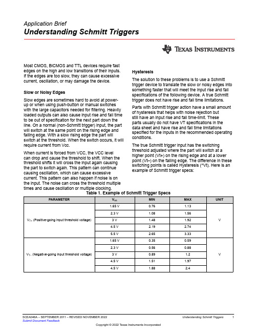
Application BriefUnderstanding Schmitt Triggers Most CMOS, BiCMOS and TTL devices require fastedges on the high and low transitions of their inputs. If the edges are too slow, they can cause excessive current, oscillation, or may damage the device.Slow or Noisy EdgesSlow edges are sometimes hard to avoid at power-up or when using push-button or manual switches with the large capacitors needed for filtering. Heavily loaded outputs can also cause input rise and fall time to be out of specification for the next part down the line. On a normal (non-Schmitt trigger) input, the part will switch at the same point on the rising edge and falling edge. With a slow rising edge the part will switch at the threshold. When the switch occurs, it will require current from Vcc.When current is forced from VCC, the VCC levelcan drop and cause the threshold to shift. When the threshold shifts it will cross the input again causing the part to switch again. This pattern can continue causing oscillation, which can cause excessive current. This pattern can also happen if noise is on the input. The noise can cross the threshold multiple times and cause oscillation or multiple clocking.HysteresisThe solution to these problems is to use a Schmitt trigger device to translate the slow or noisy edges into something faster that will meet the input rise and fall specifications of the following device. A true Schmitt trigger does not have rise and fall time limitations. Parts with Schmitt trigger action have a small amount of hysteresis that helps with noise rejection butstill have an input rise and fall time-limit. Theseparts usually do not have VT specifications in the data sheet and have rise and fall time limitations specified for the inputs in the recommended operating conditions.The true Schmitt trigger input has the switching threshold adjusted where the part will switch at a higher point (Vt+) on the rising edge and at a lower point (Vt–) on the falling edge. The difference in these switching points is called Hysteresis (^Vt). Here is an example of Schmitt trigger specs:SCEA046A – SEPTEMBER 2011 – REVISED NOVEMBER 2022Submit Document FeedbackUnderstanding Schmitt Triggers1It is important to remember (Vt+ max) = Vih and (VT–min) = Vil. In the specs, multiple limits are relatedto the Schmitt trigger inputs. All of the limits areimportant for different reasons. On the input risingedge, the part will switch between (Vt+ min) and (Vt+max). On the falling edge, the part will switch between(Vt– max) and (Vt– min). The part will not switchbetween (Vt– max) and (Vt+ min). This is importantfor noise rejection.The hysteresis is the delta between where the partswitches on the rising edge and where it switches onthe falling edge. The hysteresis will be at least the minand no more than the max (^Vt) spec.Figure 1.In the figure above, the input levels Vih and Vil mustbe greater than (VT+ max) and less than (VT– min)to ensure the part will switch. The switching points onthe above plot are separated to give a clearer visualpicture. In reality, the (VT+ min) and (VT– max) mayoverlap.Input VoltageOne common misconception is that the currentconsumption will be less when switching a slow signalinto a Schmitt trigger. This misconception is partly truebecause the Schmitt trigger prevents oscillation whichcan draw a lot of current; however, the Icc currentmay still be higher due to the amount of time the inputis not at the rail. This is Delta Icc. Delta Icc is wherethe inputs are not at the rails and upper or lower drivetransistors are partially on. The plot below shows Iccacross the input voltage sweep.Figure 2. Supply Current as a Function of InputVoltageSine WavesUse Schmitt triggers to translate a sine wave into asquare wave as shown in this oscillator application.Also, use Schmitt triggers to speed up a slow ornoisy input, or clean up an input, as in the switchde-bouncer circuit.2Understanding Schmitt Triggers SCEA046A – SEPTEMBER 2011 – REVISED NOVEMBER 2022Submit Document FeedbackFigure 3. Oscillator Application Using SchmittTrigger InverterFigure 4. Switch De-bouncer Using SchmittTrigger InverterConclusionSchmitt triggers can be used to change a sine wave into a square wave, clean up noisy signals, andconvert slow edges to fast edges.Figure 5. Sine Wave to Square WaveFigure 6. Clean Noisy SignalsFigure 7. Convert Slow EdgesWe specify the part will switch on the rising edge between (VT+ min) and (VT+ max). We specify the part will switch on the falling edge between (VT– max) and (VT– min).Between (VT+ min) and (VT– max), we specify the part will not switch. This specification can be used for noise rejection. These 2 limits can overlap.We specify a minimum amount of hysteresis as delta VT min.•Vih = (VT+ max)•Vil = (VT– min)Texas Instrument Schmitt trigger functions areavailable in most all technology families from the 30 year old 74XX family to the latest AUP1T family. These two Schmitt-trigger functions are available in most families:•14 for inverting Schmitt trigger•17 for non-inverting Schmitt triggerTexas Instrument also has a complete line of little logic products with Schmitt trigger inputs.ConfigurationsSN74LVC1G57, SN74LVC1G58, SN74LVC1G97, SN74LVC1G98, SN74LVC1G99 SN74AUP1G57, SN74AUP1G58, SN74AUP1G97, SN74AUP1G98, SN74AUP1G99Low to High TranslatorsSN74AUP1T02, SN74AUP1T04, SN74AUP1T08, SN74AUP1T14, SN74AUP1T157, SN74AUP1T158, SN74AUP1T17, SN74AUP1T32, SN74AUP1T86SCEA046A – SEPTEMBER 2011 – REVISED NOVEMBER 2022Submit Document FeedbackUnderstanding Schmitt Triggers 3IMPORTANT NOTICE AND DISCLAIMERTI PROVIDES TECHNICAL AND RELIABILITY DATA (INCLUDING DATA SHEETS), DESIGN RESOURCES (INCLUDING REFERENCE DESIGNS), APPLICATION OR OTHER DESIGN ADVICE, WEB TOOLS, SAFETY INFORMATION, AND OTHER RESOURCES “AS IS” AND WITH ALL FAULTS, AND DISCLAIMS ALL WARRANTIES, EXPRESS AND IMPLIED, INCLUDING WITHOUT LIMITATION ANY IMPLIED WARRANTIES OF MERCHANTABILITY, FITNESS FOR A PARTICULAR PURPOSE OR NON-INFRINGEMENT OF THIRD PARTY INTELLECTUAL PROPERTY RIGHTS.These resources are intended for skilled developers designing with TI products. You are solely responsible for (1) selecting the appropriate TI products for your application, (2) designing, validating and testing your application, and (3) ensuring your application meets applicable standards, and any other safety, security, regulatory or other requirements.These resources are subject to change without notice. TI grants you permission to use these resources only for development of an application that uses the TI products described in the resource. Other reproduction and display of these resources is prohibited. No license is granted to any other TI intellectual property right or to any third party intellectual property right. TI disclaims responsibility for, and you will fully indemnify TI and its representatives against, any claims, damages, costs, losses, and liabilities arising out of your use of these resources.TI’s products are provided subject to TI’s Terms of Sale or other applicable terms available either on or provided in conjunction with such TI products. TI’s provision of these resources does not expand or otherwise alter TI’s applicable warranties or warranty disclaimers for TI products.TI objects to and rejects any additional or different terms you may have proposed.Mailing Address: Texas Instruments, Post Office Box 655303, Dallas, Texas 75265Copyright © 2022, Texas Instruments Incorporated。
品质专业英语大全零件材料类的专有名词

品质专业英语大全零件材料类的专有名词CPU: central processing unit(中央处理器)IC: Integrated circuit(集成电路)Memory IC: Memory Integrated circuit(记忆集成电路)RAM: Random Access Memory(随机存取存储器)DRAM: Dynamic Random Access Memory(动态随机存取存储器)SRAM: Staic Random Access Memory(静态随机存储器)ROM: Read-only Memory(只读存储器)EPROM:Electrical Programmable Read-only Memory(电可抹只读存诸器)EEPROM: Electrical Erasbale Programmable Read-only Memory(电可抹可编程只读存储器)CMOS: Complementary Metal-Oxide-Semiconductor(互补金属氧化物半导体)BIOS: Basic Input Output System(基本输入输出系统)Transistor:电晶体LED:发光二极体Resistor:电阻Variator:可变电阻Capacitor:电容Capacitor array:排容Diode:二极体Transistor:三极体Transformer:变压器(ADP)Oscillator:频率振荡器(0sc)Crystal:石英振荡器XTAL/OSC:振荡产生器(X)Relay:延时器Sensor:感应器Bead core:磁珠Filter:滤波器Flat Cable:排线Inductor:电感Buzzer:蜂鸣器Socket:插座Slot:插槽Fuse:熔断器Current:电流表Solder iron:电烙铁Magnifying glass:放大镜Caliper:游标卡尺Driver:螺丝起子Oven:烤箱TFT:液晶显示器Oscilloscope:示波器Connector:连接器PCB:printed circuit board(印刷电路板)PCBA: printed circuit board assembly(电路板成品)PP:并行接口HDD:硬盘FDD:软盘PSU:power supply unit(电源供应器)SPEC:规格Attach:附件Case: 机箱,盖子Cover:上盖Base:下盖Bazel:面板(panel)Bracket:支架,铁片Lable:贴纸Guide:手册Manual:手册,指南Card:网卡Switch:交换机Hub:集线器Router:路由器Sample:样品Gap:间隙Sponge:海绵Pallet:栈板Foam:保利龙Fiber:光纤Disk:磁盘片PROG:程序Barcode:条码System:系统System Barcode:系统条码M/B:mother board:主板CD-ROM:光驱FAN:风扇Cable:线材Audio:音效K/B:Keyboard(键盘)Mouse:鼠标Riser card:转接卡Card reader:读卡器Screw:螺丝Thermal pad:散热垫Heat sink:散热片Rubber:橡胶垫Rubber foot:脚垫Bag:袋子Washer:垫圈Sleeve:袖套Config:机构Label hi-pot:高压标签Firmware label:烧录标签Metal cover:金属盖子Plastic cover:塑胶盖子Tape for packing:包装带Bar code:条码Tray:托盘Collecto:集线夹Holder:固定器,L铁Connecter:连接器IDE:集成电路设备,智能磁盘设备SCSI:小型计算机系统接口Gasket:导电泡棉AGP:加速图形接口PCI:周边组件扩展接口LAN:局域网USB:通用串形总线架构Slim:小型化COM:串型通讯端口LPT:打印口,并行口Power cord:电源线I/O:输入,输出Speaker:扬声器EPE:泡棉Carton:纸箱Button:按键,按钮Foot stand:脚架部门名称的专有名词QS:Quality system品质系统CS:Coutomer Sevice 客户服务QC:Quality control品质管理IQC:Incoming quality control 进料检验LQC:Line Quality Control 生产线品质控制IPQC:In process quality control 制程检验FQC:Final quality control 最终检验OQC:Outgoing quality control 出货检验QA:Quality assurance 品质保证SQA:Source(supplier) Quality Assurance 供应商品质保证(VQA)CQA:Customer Quality Assurance客户质量保证PQA rocess Quality Assurance 制程品质保证QE:Quality engineer 品质工程CE:component engineering零件工程EE:equipment engineering设备工程ME:manufacturing engineering制造工程TE:testing engineering测试工程PPE roduct Engineer 产品工程IE:Industrial engineer 工业工程ADM: Administration Department行政部RMA:客户退回维修CSDI:检修PC:producing control生管MC:mater control物管GAD: General Affairs Dept总务部A/D: Accountant /Finance Dept会计LAB: Laboratory实验室DOE:实验设计HR:人资PMC:企划RD:研发W/H:仓库SI:客验PD: Product Department生产部PA:采购(PUR: Purchaing Dept)SMT:Surface mount technology 表面粘着技术MFG:Manufacturing 制造MIS:Management information system 资迅管理系统DCC:document control center 文件管制中心厂内作业中的专有名词QT:Quality target品质目标QP:Quality policy目标方针QI:Quality improvement品质改善CRITICAL DEFECT:严重缺点(CR)MAJOR DEFECT:主要缺点(MA)MINOR DEFECT:次要缺点(MI)MAX:Maximum最大值MIN:Minimum最小值DIA iameter直径DIM imension尺寸LCL:Lower control limit管制下限UCL:Upper control limit管制上限EMI:电磁干扰ESD:静电防护EPA:静电保护区域ECN:工程变更ECO:Engineering change order工程改动要求(客户)ECR:工程变更需求单CPI:Continuous Process Improvement 连续工序改善Compatibility:兼容性Marking:标记DWG rawing图面Standardization:标准化Consensus:一致Code:代码ZD:Zero defect零缺点Tolerance:公差Subject matter:主要事项Auditor:审核员BOM:Bill of material物料清单Rework:重工ID:identification识别,鉴别,证明PILOT RUN: (试投产)FAI:首件检查FPIR:First Piece Inspection Report首件检查报告FAA:首件确认SPC:统计制程管制CP: capability index(准确度)CPK: capability index of process(制程能力)PMP:制程管理计划(生产管制计划)MPI:制程分析DAS efects Analysis System 缺陷分析系统PPB:十亿分之一Flux:助焊剂P/N:料号L/N:Lot Number批号Version:版本Quantity:数量Valid date:有效日期MIL-STD:Military-Standard军用标准ICT: In Circuit Test (线路测试)ATE:Automatic Test Equipment自动测试设备MO: Manafacture Order生产单T/U: Touch Up (锡面修补)I/N:手插件P/T:初测F/T: Function Test (功能测试-终测)AS 组立P/K:包装TQM:Total quality control全面品质管理MDA:manufacturing defect analysis制程不良分析(ICT) RUN-IN:老化实验HI-pot:高压测试FMI:Frequency Modulation Inspect高频测试DPPM: Defect Part Per Million(不良率的一种表达方式:百万分之一) 1000PPM即为0.1% Corrective Action: (CAR改善对策)ACC:允收REJ:拒收S/S:Sample size抽样检验样本大小SI-SIV:Special I-Special IV特殊抽样水平等级CON:Concession / Waive特采ISO:国际标准化组织ISA:Industry Standard Architecture工业标准体制结构OBA:开箱稽核FIFO:先进先出PDCA:管理循环Plan do check action计划,执行,检查,总结WIP:在制品(半成品)S/O: Sales Order (业务订单)P/O: Purchase Order (采购订单)P/R: Purchase Request (请购单)AQL:acceptable quality level允收品质水准LQL;Limiting quality level最低品质水准QVL:qualified vendor list合格供应商名册AVL :认可的供货商清单(Approved Vendor List)QCD: Quality cost delivery(品质,交期,成本)MPM:Manufacturing project management制造专案管理KPI:Key performance indicate重要绩效指标MVT:Manufacturing Verification Test制造验证试产Q/R/S:Quality/Reliability/Service质量/可靠度/服务STL:ship to line(料到上线)NTF:No trouble found误判CIP:capacity improvement plan(产能改善计划)MRB:material review board(物料审核小组)MRB:Material reject bill退货单JIT:just in time(即时管理)5S:seiri seiton seiso seiketsu shitsuke(整理,整顿,清扫,清洁,修养)SOP:standard operation process(标准作业程序)SIP:Specification inspection process制程检验规格TOP: Test Operation Process (测试作业流程)WI: working instruction(作业指导书)SMD:surface mounting device(表面粘着原件)FAR:failure aualysis report故障分析报告CAR:Corrective action report改善报告BPR:企业流程再造(Business Process Reengineering)ISAR :首批样品认可(Initial Sample Approval Request)-JIT:实时管理(Just In Time)QCC :品管圈(Quality Control Circle)Engineering Department (工程部)TQEM: Total Quality Environment Management(全面品质环境管理)PD: Production Department (制造)LOG: Logistics (后勤支持)Shipping: (进出口)AOQ:Average Output Quality平均出货质量AOQL:Average Output Quality Level平均出货质量水平FMEA:failure model effectiveness analysis失效模式分析CRB: Change Review Board (工程变更会议)CSA:Customer Simulate Analysis客户模拟分析SQMS:Supplier Quality Management System供应商品质管理系统QIT: Quality Improvement Team 品质改善小组QIP:Quality Improvement Plan品质改善计划CIP:Continual Improvement Plan持续改善计划M.Q.F.S: Material Quality Feedback Sheet (来料品质回馈单) SCAR: Supplier Corrective Action Report (供货商改善对策报告)8D Sheet: 8 Disciplines sheet ( 8D单)PDCA:PDCA (Plan-Do-Check-Action) (管理循环)MPQ: Material Packing Quantity (物料最小包装量)DSCN: Delivery Schedule Change Notice (交期变更通知) QAPS: Quality Assurance Process Sheet (品质工程表)DRP :运销资源计划(Distribution Resource Planning)DSS:决策支持系统(Decision Support System)EC :电子商务(Electronic Commerce)EDI :电子资料交换(Electronic Data Interchange)EIS :主管决策系统(Excutive Information System)ERP:企业资源规划(Enterprise Resource Planning)FMS :弹性制造系统(Flexible Manufacture System)KM :知识管理(Knowledge Management)4L :逐批订购法(Lot-for-Lot)LTC :最小总成本法(Least Total Cost)LUC :最小单位成本(Least Unit Cost)MES :制造执行系统(Manufacturing Execution System)MPS :主生产排程(Master Production Schedule)MRP :物料需求规划(Material Requirement Planning)MRPⅡ:制造资源计划(Manufacturing Resource Planning)OEM :委托代工(Original Equipment Manufacture)ODM :委托设计与制造(Original Design & Manufacture)OLAP:线上分析处理(On-Line Analytical Processing)OLTP:线上交易处理(On-Line Transaction Processing)OPT :最佳生产技术(Optimized Production Technology)PDCA:PDCA管理循环(Plan-Do-Check-Action)PDM:产品数据管理系统(Product Data Management))RCCP:粗略产能规划(Rough Cut Capacity Planning)SCM :供应链管理(Supply Chain Management)SFC :现场控制(Shop Floor Control)TOC:限制理论(Theory of Constraints)TQC :全面品质管制(Total Quality Control)FYI/R:for your information/reference仅供参考ASAP:尽快S/T:Standard time标准时间TPM:total production maintenance:全面生产保养ESD Wrist strap:静电环IT:information technology信息技术,资讯科学CEO:Chief Executive Officer执行总裁COO:Chief Operaring Officer首席业务总裁SWOT:Strength,Weakness,Opportunity,Threat优势﹐弱点﹐机会﹐威胁Competence:专业能力Communication:有效沟通Cooperation:统御融合Vibration Testing:振动测试IDP:Individual Development Plan个人发展计划MRP:Material Requirement Planning物料需求计划MAT'S:Material材料LRR:Lot Reject Rate批退率ATIN:Attention知会3C:Computer ,Communication , Consumer electronic消费性电子5W1H:When , Where , Who , What , Why , How5M: Man , Machine , Material , Method , Measurement人,机器,材料,方法,测量4MIE: Man,Material,Machine,Method,Environment人力,物力,财务,技术,时间(资源)7M1I: Manpower , Machine , Material , Method, Market , Management , Money , Information 人力,机器,材料,方法, 市场,管理,资金,资讯1 Accuracy 准确度2 Action 行动3 Activity 活动4 Analysis Covariance 协方差分析5 Analysis of Variance 方差分析6 Approved 承认7 Attribute 计数值8 Average 平均数9 Balance sheet 资产负债对照表10 Binomial 二项分配11 Brainstorming Techniques 脑力风暴法12 Cause and Effect Matrix 因果图(鱼骨图)13 CL:Center Line 中心线14 Check Sheets 检查表15 Complaint 投诉16 Conformity 合格(符合)17 Control 控制18 Control chart 控制(管制)图19 Correction 纠正20 Correlation Methods 相关分析法21 CPI: continuous Process Improvement 连续工序改善22 Cross Tabulation Tables 交叉表23 CS: Customer Service 客(户)服(务)中心24 DSA: Defects Analysis System 缺陷分析系统25 Data 数据Description:品名26 DCC: Document Control Center 文控中心27 Decision 决策、判定28 Defects per unit 单位缺点数29 Description 描述30 Device 装置31 Do 执行32 DOE: Design of Experiments 实验设计33 Element 元素34 Engineering Technology 工程技35 Environmental 环境36 Equipment 设备37 Estimated accumulative frequency 计算估计累计数38 E Equipment Variation 设备变异39 External Failure 外部失效,外部缺陷40 FA: Failure Analysis 失效分析41 Fact control 事实管理42 Fatigue 疲劳43 FMEA: Failure Mode and Effect Analysis失效模式与效果分析44 FP First-Pass Yield (第一次通过)合格率45 FQA: Final Quality Assurance 最终品质保证46 FQC: Final Quality control 最终品质控制47 Gauge system 测量系统48 Grade 等级49 Histogram 直方图50 Improvement 改善51 Initial review 先期审查52 Inspection 检验53 Internal Failure 内部失效、内部缺陷54 IPQC: In Process Quality Control 制程品质控制55 IQC: Incomming Quality Control 来料品质控制56 IS International Organization for Standardization 国际标准化组织57 LCL: Lower Control limit 管制下限58 LQC: Line Quality Control 生产线品质控制59 LSL: Lower Size Limit 规格下限60 Machine 机械61 Manage 管理62 Materials 物料63 Measurement 测量64 Median 中位数65 MSA: Measurement System Analysis 测量系统分析66 Occurrence 发生率67 Operation Instruction 作业指导书68 Organization 组织69 Parto 柏拉图70 PPM arts per Million (百万分之)不良率71 Plan 计划72 Policy 方针73 Population 群体74 PQA: Process Quality Assurance 制程品质保证75 Practice 实务(践)76 Prevention 预防77 Probability 机率78 Probability density function 机率密度函数79 Procedure 流程80 Process 过程81 Process capability analysis 制程能力分析(图)82 Process control and Process capability制程管制与制程能力83 Product 产品84 Production 生产85 Projects 项目86 QA: Quality Assurance 品质保证87 QC: Quality Control 品质控制88 QE: Quality Engineering 品质工程89 QFD: Quality Function Desgin 品质机能展开(法)90 Quality 质量91 Quality manual 品质手册92 Quality policy 品质政策(质量方针)93 Random experiment 随机试验94 Random numbers 随机数95 R:Range 全距(极差)96 Reject 拒收97 Repair 返修98 Repeatusility 再现性99 Reproducibility 再生性100 Requirement 要求101 Responsibilities 职责102 Review 评审103 Reword 返工104 Rolled yield 直通率105 RPN: Risk Priority Number 风险系数106 Sample 抽样,样本107 Sample space 样本空间108 Sampling with replacement 放回抽样109 Sampling without replacement 不放回抽样110 Scatter diagram 散布图分析111 Scrap 报废112 Simple random sampling 简单随机取样113 Size 规格114 SL: Size Line 规格中心线115 Stratified random sampling 分层随机抽样116 SOP: Standard Operation Procedure 标准作业书117 SPC: Statistical Process Control 统计制程管制118 Specification 规范119 SQA: Source(Supplier) Quality Assurance 供货商品质保证120 Stage sampling 分段随机抽样121 Standard Deviation 标准差122 Sum of squares 平方和123 Taguchi-method 田口(试验)方法124 Theory 原理125 TQC: Total Quality Control 全面品质控制126 TQM: Total Quality Management 全面品质管理127 Traceability 追溯128 Training 培训129 UCL: Upper Control Limit 管制(控制)上限130 USL: Upper Size Limit 规格上限131 Validation 确认132 Variable 计量值133 Verification 验证134 Version 版本135 VOC: Voice of Customer 客户需求136 VOE: Voice of Engineer 工程需求137 Inventory stock report:庫存清单报告138 Sales order report:出货报告质量人员名称类QC quality control 品质管理人员FQC final quality control 终点质量管理人员IPQC in process quality control 制程中的质量管理人员OQC output quality control 最终出货质量管理人员IQC incoming quality control 进料质量管理人员TQC total quality control 全面质量管理POC passage quality control 段检人员QA quality assurance 质量保证人员OQA output quality assurance 出货质量保证人员QE quality engineering 质量工程人员质量保证类FAI first article inspection 新品首件检查FAA first article assurance 首件确认CP capability index 能力指数CPK capability process index 模具制程能力参数SSQA standardized supplier quality audit 合格供货商质量评估FMEA failure model effectiveness analysis 失效模式分析FQC运作类AQL Acceptable Quality Level 运作类允收质量水平S/S Sample size 抽样检验样本大小ACC Accept 允收REE Reject 拒收CR Critical 极严重的MAJ Major 主要的MIN Minor 轻微的Q/R/S Quality/Reliability/Service 质量/可靠度/服务P/N Part Number 料号L/N Lot Number 批号AOD Accept On Deviation 特采UAI Use As It 特采FPIR First Piece Inspection Report 首件检查报告PPM Percent Per Million 百万分之一制程统计品管专类SPC Statistical Process Control 统计制程管制SQC Statistical Quality Control 统计质量管理GRR Gauge Reproductiveness & Repeatability 量具之再制性及重测性判断量可靠与否DIM Dimension 尺寸DIA Diameter 直径N Number 样品数其它质量术语类QIT Quality Improvement Team 质量改善小组ZD Zero Defect 零缺点QI Quality Improvement 质量改善QP Quality Policy 目标方针TQM Total Quality Management 全面质量管理RMA Return Material Audit 退料认可7QCTools 7 Quality Control Tools 品管七大手法通用之件类ECN Engineering Change Notice 工程变更通知(供货商) ECO Engineering Change Order 工程改动要求(客户) PCN Process Change Notice 工序改动通知PMP Product Management Plan 生产管制计划SIP Standard Inspection Procedure 制程检验标准程序SOP Standard Operation Procedure 制造作业规范IS Inspection Specification 成品检验规范BOM Bill Of Material 物料清单PS Package Specification 包装规范SPEC Specification 规格DWG Drawing 图面系统文件类ES Engineering Standard 工程标准CGOO China General PCE龙华厂文件IWS International Workman Standard 工艺标准ISO International Standard Organization 国际标准化组织GS General Specification 一般规格部类PMC Production & Material Control 生产和物料控制PCC Product control center 生产管制中心PPC Production Plan Control 生产计划控制MC Material Control 物料控制DC Document Center 资料中心QE Quality Engineering 质量工程(部)QA Quality Assurance 质量保证(处)QC Quality Control 质量管理(课)PD Product Department 生产部LAB Laboratory 实验室IE Industrial Engineering 工业工程R&D Research & Design 设计开发部生产类PCs Pieces 个(根,块等)PRS Pairs 双(对等)CTN Carton 卡通箱PAL Pallet/skid 栈板PO Purchasing Order 采购订单MO Manufacture Order 生产单D/C Date Code 生产日期码ID/C Identification Code (供货商)识别码SWR Special Work Request 特殊工作需求L/N Lot Number 批号P/N Part Number 料号OEM Original Equipment Manufacture 原设备制造PC Personal Computer 个人计算机CPU Central Processing Unit 中央处理器A.S.A.P As Soon As Possible 尽可能快的E-MAIL Electrical-Mail 电子邮件N/A Not Applicable 不适用QTY Quantity 数量I/O input/output 输入/输出NG Not Good 不行,不合格C=0 Critical=0 极严重不允许APP Approve 核准,认可,承认CHK Check 确认ASS'Y Assembly 装配,组装T/P True Position 真位度5WIH When, Where, Who, What, Why, How to6M Man, Machine, Material, Method, Measurement, Message4MTH Man, Material, Money, Method, Time, How 人力,物力,财务,技术,时间(资源) SQA Strategy Quality Assurance 策略质量保证DQA Design Quality Assurance 设计质量保证MQA Manufacture Quality Assurance 制造质量保证SSQA Sales and service Quality Assurance 销售及服务质量保证LRR Lot Reject Rate 批退率SPS Switching power supply 电源箱DT Desk Top 卧式(机箱)MT Mini-Tower 立式(机箱)DVD Digital Video DiskVCD Video Compact DiskLCD Liquid Crystal DisplayCAD Computer Aided DesignCAM Computer Aided ManufacturingCAE Computer Aided EngineeringPCB Printed Circuit Board 印刷电路板CAR Correction Action Report 改善报告NG Not Good 不良WDR Weekly Delivery Requirement 周出货要求PPM Percent Per Million 百万分之一TPM Total Production Maintenance 全面生产保养MRP Material Requirement Planning 物料需计划OS Operation System 操作系统TBA To Be Assured 待定,定缺D/C Drawing ChangeP/P Plans & ProcedureEMI Electrical-Music Industry 电子音乐工业Electrical Magnetic Interference 电子干扰RFI Read Frequency Input 读频输入MMC Maximum Material ConditionMMS Maximum Material SizeLMC Least Material ConditionLMS Least Material SizeLED lighting-emitting diode 发光二极管QBR Quarter Business RecordCIP Continuous improvement processFGI Forecasted Goal InventoryCNC Computerized numeral controllerB2C Business to customerB2B Business to businessAVL Approved vendor listPOP Procedure of packagingEOL End of lifeVDCS Vender defect correcting sheetPDCS Process defect correcting sheetGRN Goods receiving noteA/R Accounting receivableA/P Accounting payable专业词汇通用类president董事长operator作业员position职务general manager总经理special assistant 特助deputy manager |'depjuti| =vice manager副理deputy supervisor =vice supervisor副课长group leader组长line leader线长supervisor 课长responsible department负责单位Human Resources Department人力资源部Head count 人头数production department生产部门planning department企划部QC Section品管课stamping factory冲压厂painting factory烤漆厂molding factory成型厂administration/general affairs dept./总务部production unit生产单位meeting minutes会议记录distribution department分发单位subject主题conclusion结论decision items决议事项pre-fixed finishing date预定完成日Color management 颜色管理Visual management 目视管理production capacity生产力first count初盘first check初盘复棹second count 复盘second check复盘复核quantity of physical inventory second count 复盘点数量physical inventory盘点数量physical count quantity账面数量difference quantity差异量spare parts physical inventory list备品盘点清单cause analysis原因分析waste materials废料description品名specification 规格model机种work order工令revision版次remark备注registration登记registration card登记卡to control管制application form for purchase请购单consume, consumption消耗to notify通知to fill in填写to collect, to gather收集statistics统计cosmetic inspection standard 外观检验规范computer case 计算机外壳(组件)personal computer enclosure 计算机机箱产品front plate前板rear plate后板chassis |'∫æsi| 基座bezel panel面板Hood 上盖base pan 基座bezel 面板riser card 扩充卡flat cable 排线TOP driver cage 上磁架bottom driver cage 下磁架resin film 树脂膜raw materials原料materials物料steel plate钢板roll/coil material卷料spare parts =buffer备品plastic parts塑料件sheet metal parts/stamping parts 冲件material check list物料检查表finished product成品semi-finished product半成品good product/accepted goods/ accepted parts/good parts良品defective product/non-good parts不良品disposed goods处理品warehouse/hub仓库packing material包材basket蝴蝶竺plastic basket胶筐flow chart流程窗体production tempo生产进度现状lots of production生产批量manufacture procedure制程to revise, modify修订to switch over to, switch—to, switching over切换engineering bottleneck, project difficulty工程瓶颈glove(s)手套glove(s) with exposed fingers割手套Band-Aid创可贴Industrial alcohol工业酒精broom扫把mop拖把vacuum cleaner吸尘器rag 抹布garbage container灰箕garbage can垃圾箱garbage bag垃圾袋liaison联络单rags抹布lamp holder灯架to mop the floor拖地to clean a table擦桌子air pipe 气管delivery deadline交货期die worker模工production, to produce生产equipment设备resistance电阻beacon警示灯coolant冷却液crusher破碎机club car高尔夫球车plate电镀power button电源按键reset button重置键forklift叉车Workshop traveler 天车trailer =long vehicle拖板车Hydraulic trolley手压车hydraulic hand jack油压板车casing = containerization装箱velocity速度patent专利coordinate坐标supply and demand供求career card履历卡barricade隔板carton box纸箱to pull and stretch拉深work cell/work shop工作间sub-line支线bottleneck 瓶颈模具工程类plain die简易模pierce die冲孔模forming die成型模progressive die连续模stage die工程模compound die复合模shearing die剪边模riveting die铆合模feature die公母模male die公模female die母模cavity型控母模core模心公模die change 换模to fix a die装模to repair a die修模punch set上模座punch pad上垫板punch holder上夹板stripper pad脱料背板up stripper上脱料板upper plate上模板lower plate下模板die pad下垫板die holder下夹板die set下模座bottom block下垫脚bottom plate下托板(底板)upper supporting blank上承板upper padding plate blank上垫板top plate上托板(顶板)top block上垫脚stripping plate内外打(脱料板) outer stripper外脱料板inner stripper内脱料板lower stripper下脱料板punch冲头insert入块(嵌入件)deburring punch压毛边冲子groove punch压线冲子stamped punch字模冲子round punch圆冲子special shape punch异形冲子bending block折刀roller滚轴baffle plate挡块located block定位块supporting block for location定位支承块air cushion plate气垫板air-cushion eject-rod气垫顶杆trimming punch切边冲子stiffening rib punch = stinger 加强筋冲子ribbon punch压筋冲子reel-stretch punch卷圆压平冲子guide plate定位板sliding block滑块sliding dowel block滑块固定块die locker锁模器pressure plate =plate pinch压板thickness gauge厚薄规cutting die, blanking die冲裁模die block模块folded block折弯块sliding block滑块location pin定位销lifting pin顶料销die plate, front board模板padding block垫块stepping bar垫条panel board镶块to load a die装上模具to unload a die 御模具active plate活动板lower sliding plate下滑块板upper holder block上压块upper mid plate上中间板spring box弹簧箱spring-box eject-rod弹簧箱顶杆spring-box eject-plate弹簧箱顶板bushing block衬套cover plate盖板guide pad导料块pilot导正筒trim剪外边pierce剪内边pocket for the punch head挂钩槽slug hole废料孔radius半径shim/wedge/heel/pad/spacer/gasket楔子torch-flame cut火焰切割set screw止付螺丝form block折刀round pierce punch =die button圆冲子shape punch =die insert异形子stock located block定位块metal plate钣金miller铣床grinder磨床tolerance公差score =groove压线sliding block滑块lathe车active plate活动板baffle plate挡块cover plate盖板groove punch压线冲子air-cushion eject-rod气垫顶杆spring-box eject-plate弹簧箱顶板capability能力parameter参数factor系数driller钻床set up die架模height of die setting up架模高度analog-mode device类模器inner guiding post内导柱inner hexagon screw内六角螺钉dowel pin固定销coil spring弹簧lifter pin顶料销eq-height sleeves =spool等高套筒pin销lifter guide pin浮升导料销guide pin导正销wire spring圆线弹簧outer guiding post外导柱stop screw止付螺丝located pin定位销outer bush外导套press specification冲床规格die height闭模高度flow mark流痕welding mark溶合痕post screw insert螺纹套筒埋值self tapping screw自攻螺丝stripper plate脱料板piston活塞handle mold手持式模具flash mold溢流式模具positive mold挤压式模具split mold分割式模具die lifter举模器top stop上死点bottom stop下死点one stroke一行程to continue, cont.连动to grip(material)吸料location lump, locating piece, location block定位块reset复位to file burr 锉毛刺embedded lump |in'bed| mp|镶块 |lstamping-missing漏冲to tight a bolt拧紧螺栓to loosen a bolt拧松螺栓punched hole冲孔to cut edge =side cut =side scrap 切边to bending折弯to pull, to stretch拉伸engraving, to engrave刻印stamping 油印to stake铆合designing, to design设计design modification 设计修改成gauge(or jig)治具pedal踩踏板stopper阻挡器flow board流水板torque扭矩spline =the multiple keys花键quenching淬火tempering回火annealing退火carbonization碳化alloy合金tungsten high speed steel钨高速的moly high speed steel钼高速的forming成型(抽凸,冲凸)draw hole抽孔bending折弯emboss凸点dome凸圆semi-shearing半剪stamp mark冲记号deburr or coin压毛边punch riveting冲压铆合side stretch侧冲压平reel stretch卷圆压平groove压线stamp letter冲字(料号)tick-mark nearside正面压印tick-mark farside反面压印冲压类punch, press冲punching machine 冲床hydraulic machine油压机jack升降机decoiler整平机manufacture management制造管理stamping, press冲压feeder送料机rack, shelf, stack料架taker取料机to reverse material 翻料to load material上料to unload material卸料to return material/stock to退料scraped |'skræpid|报废scrape ..v.刮;削robot机械手production line流水线packaging tool打包机packaging打包成型类well type蓄料井insulated runner绝缘浇道方式hot runner热浇道runner plat浇道模块valve gate阀门浇口band heater环带状的电热器spindle阀针spear head刨尖头slag well冷料井cold slag冷料渣air vent排气道welding line熔合痕eject pin顶出针knock pin顶出销return pin回位销反顶针sleeve套筒stripper plate脱料板insert core放置入子runner stripper plate浇道脱料板guide pin导销eject rod (bar)(成型机)顶业捧subzero深冷处理three plate三极式模具runner system浇道系统stress crack应力电裂orientation定向sprue gate射料浇口,直浇口nozzle射嘴sprue lock pin料头钩销(拉料杆) slag well冷料井side gate侧浇口edge gate侧缘浇口tab gate搭接浇口film gate薄膜浇口flash gate闸门浇口slit gate缝隙浇口fan gate扇形浇口dish gate因盘形浇口diaphragm gate隔膜浇口ring gate环形浇口submarine gate潜入式浇口tunnel gate隧道式浇口pin gate针点浇口runner less无浇道sprue less 无射料管方式long nozzle延长喷嘴方式spur浇口;溶waste废料board广告牌sliding rack滑料架to impose lines压线to compress, compressing压缩character die字模to feed, feeding送料material change, stock change材料变更feature change 特性变更prepare for, make preparations for 准备rotating speed, revolution转速abnormal handling异常处理组装类Assembly line组装线Layout布置图Conveyer流水线运输带Rivet machine拉钉机Rivet gun拉钉枪Screw driver起子Electric screw driver电动起子Hydraulic machine 液压机Pneumatic screw driver气动起子automation自动化to stake, staking, riveting铆合add lubricant oil加润滑油argon welding氩焊cylinder油缸robot机械手conveying belt输送带transmission rack输送架to draw holes抽孔bolt螺栓nut 螺母screw 螺丝identification tag标示单screwdriver plug起子插座automatic screwdriver电动启子to move, to carry, to handle搬运be put in storage入库packing包装staker = riveting machine铆合机fit together组装在一起fasten锁紧(螺丝)fixture 夹具(治具)pallet/skid栈板barcode条形码barcode scanner条形码扫描仪fuse together熔合fuse machine/heat stake热熔机processing, to process加工delivery, to deliver 交货to return delivery to. to send delivery back to return of goods退货easily damaged parts易损件standard parts标准件to lubricate润滑spring 弹簧spare tools location/buffer手工备品仓spare molds location模具备品仓tox machine自铆机烤漆类phosphate皮膜化成viscosity涂料粘度alkalidipping脱脂main manifold主集流脉organic solvent有机溶剂demagnetization去磁;消磁high-speed transmission高速传递heat dissipation热传rack上料volatile挥发性degrease脱脂rinse水洗alkaline etch龄咬desmot剥黑膜D.I. rinse纯水次Chromate铬酸处理Anodize阳性处理seal封孔scraped products报放品disposed products处理品dismantle the die折模auxiliary function辅助功能heater band 加热片thermocouple热电偶derusting machine除锈机degate打浇口dryer烘干机induction感应induction light感应光response =reaction =interaction感应ram连杆edge finder巡边器concave凸convex凹cold slug冷块blush 导色gouge沟槽;凿槽satin texture段面咬花witness line证示线grit沙砾granule =pellet =grain细粒sand blasting喷沙grit maker抽粒机cushion缓冲fillet镶;嵌边roller pin formality滚针形式cam driver铡楔shank摸柄crank shaft曲柄轴品质类qualified products, up-to-grade products良品defective products, not up-to-grade products不良品defective product box不良品箱poor processing 制程不良poor incoming part来件不良exposed metal/bare metal金属裸露excessive defect过多的缺陷critical defect极严重缺陷major defect主要缺陷。
CE523NOTESONSCREENS
CE 523 NOTES ON SCREENSWastewaters may contain coarse suspended and floating matter that may damage or interfere with the operation of pumps and other equipment. This material is usually removed by simple screening devices, which represents the most eco nomical form of treatmentIn water supply systems, screens are usually located at intakes from rivers, lakes or open storage reservoirs, where they serve to prevent the entry of logs and sticks or even fish and animals (see introductory presentation). In sewerage systems, screens are sometimes provided at the inlet to sewage pumping stations where rags, paper and other coarse materials could cause damage by fouling pump impellers. Also, screens are placed on sewer overflow structures where it is desirable to prevent coarse materials from fouling the receiving environment. Screens are usually installed at the inlets to wastewater treatment plants to remove materials that may otherwise become entangled in pumps, scrapers and aeration devices, or may foul weirs and channels.Classification of screensScreens may be classified variously according to: their clear opening size (as coarse, medium or fine); their configuration (racks, bar screens or mesh screens); the method used to clean the entrapped material from the screen surface (manually-raked or mechanically-raked, or water-jet cleaned); and also according to whether the screen surface is fixed or moving. Combined screening and maceration devices are sometimes used at wastewater treatment works.Fixed screensRacks and bar screens These are the simplest forms, and are widely used at inlets to wastewater treatment plants, and on river intakes for water supplies.Bar screens consist of parallel metal bars with 20 to 60 mm clear openings in coarse screens, and 10 to 20 mm clear openings in fine to medium screens. Fine screens are usually preceded by coarse screens in order to prevent the risk of damage by large objects, or excessive head loss as screenings accumulate.Bar screens may be satisfactorily cleaned by manual raking in small installations (Figure1a-i). Large installations, however, are generally provided with mechanical devices for removing screenings at regular intervals (Figure 1a-ii). Such devices may be operated either by time clocks or by pressure-sensing probes, and are activated when the head loss across the screen becomes excessive. A large number of proprietary screens with mechanical rakes is currently available. In most cases, manufacturers provide design charts to facilitate selection of appropriate screen sizes.Mesh screens These are used mainly in water supply and water treatment installations. They have square openings ranging in size from 1 to 25 mm or greater, according to design requirements. Most fine mesh screens are used in locations where relatively small amounts of material are to be removed, and these usually are manually cleaned. Suchscreens, for example, may follow bar screens on water intakes in order to prevent small fish from being drawn into the intake.Moving screensDrum screen This is a continuous screening device consisting of a hollow drum, usually 2 to 5 m in diameter, which rotates about its horizontal axis (Figure 1b). One end of the drum is closed. Water enters the drum through the opposite end and passes out through perforations or mesh openings in the drum’s periphery. As the drum rotates, screenings caught on it are carried clear of the water surface and are deposited in a collecting trough. Water jets help to clean the entrapped material from the screen surface.Disc screen This consists of a large rotating partly immersed metal disc, often set at an angle of about 30 to the vertical. Solids caught on the face of the disc are carried to the top where they are removed by revolving brushes.Fine belt screens These are made of flexible woven wire mesh. Although only rarely used in the treatment of water and municipal sewage, they are commonly used in industrial wastes treatment. The rotation of the screen is an aid to cleaning. Some belt screens are vibrated to increase efficiency and prevent clogging when screening out fine material, such as spent grain from a distillery or fine organic wastes from a canning factory.Medium belt screens These are used for continuous operation to remove floating and suspended debris from water supply intakes. They consist of sections of mesh attached to frames which are hinged together and mounted on a chain belt (Figure 1a-ii). Microstrainers These are a development of the drum screen in which the screening fabric consists of woven stainless steel micromesh (Figure 1c). Micromeshes, with apertures ranging from 15 to 64 mm, are used to remove very fine suspended matter from feed water. They are usually 0.8 to 3 m in diameter and rotate at a maximum peripheral speed of 0.5 m/s. Effective cleaning of microstrainers requires high-pressure water jets using good quality water. To control the growth of slime bacteria, which would rapidly clog the micromesh, the drum surface can be bathed in ultraviolet light.The principal application of microstraining is the pre-treatment of some types of water supply, prior to using other treatment processes. In the case of some good-quality upland waters, it may be all the treatment necessary for removing some types of algae and other planktonic organisms. In wastewater treatment, microstrainers are also used at a tertiary stage to further improve a good-quality secondary effluent by removing suspended solids escaping from the final sedimentation tanks. In these applications, microstrainers fulfil a function more usually associated with filters than with conventional screens.Loading rates of 350 to 2 300 m3/m2.d have been claimed for microstrainers, but in any particular application the design should be based on tests carried out on the water to be treated. For design purposes, conventional water analyses, such as those used for suspended solids, provide inadequate information since the number, size and shape of particles all affect the rate of removal by microstrainers .Wedgewire screens See figure below and / See also figure at end.With sharp edges (almost no radius) and avery smooth surface, the ‘V’ shape profilewires ensure that the solid particles make only2 points contact with the screen surface..Particles do not get trapped in the slot opening and do not have any problem sliding on the surface. As a result,clogging of the slot opening is none, the blinding effect gets minimized and the open area available remains constantWedgewire screens are superior for retaining media, filtering, and sizing. In comparison with wire mesh and perforated metal, wedge wire continuous slot screens have more open area, have very precise openings, are stronger and more durable, are virtually non-clogging and reduce media abrasion. Wire mesh and perforated metal may be less expensive initially, but wedgewire screens offer easier installation and long -term operating and cost benefits. Wedge wire screens have maximum design flexibility, can be constructed in a wide variety of shapes and sizes from a variety of corrosion resistant alloys such as type 304, 316, 316L, 321, and 410S stainless steels, as well as nickel alloys such as C-276.Underdrains of filtersand packed columnsIn order to retain finermaterial within largeprocess units, there is aneed for distributors ornozzles or screens.Examples of these areshown in the figure atthe right.Disposal of screeningsScreenings removed at water supply intakes usually comprise leaves, sticks and other vegetable matter which are relatively inoffensive and may be returned to the river downstream of the intake. Wastewater screenings are often heavily contaminated with faecal matter and need to be carefully disposed of as quickly as possible – usually byburial, incineration, or maceration and returned to the flow.Design of screensThe main factors to be considered in screen design are: the strength and durability of the screening medium; the clear screen area; maximum flow velocity through the screen apertures so that screenings will not be dislodged; minimum velocity in the approach channel to prevent settlement of suspended matter on the channel floor, and the head loss through the screen. In most cases mild steel is satisfactory for making screens but other materials may need to be considered in abnormally corrosive environments. The strength of the screen media should be sufficient to withstand impact of large floating objects and the forces that may be generated by mechanical cleaning devices.Generally, the velocity through screen apertures should not exceed 0.6 to 1.0 m/s, depending upon the nature of the materials to be removed and their susceptibility to being forced through the screen at higher flow velocity. To prevent deposition of sand and other suspended matter in approach channels, a minimum flow velocity is required. This is related to both the size and density of the suspended impurities and to the flow velocity in the channel from which the water or wastewater was drawn. A minimum velocity of 0.3 to 0.4 m/s is usually sufficient to prevent excessive accumulation of settled materials in approach channels.Head loss through screensThe minimum head loss through clean screens can be estimated by considering the screen to approximate an orifice or a short conduit, or even by applying a minor loss expression. A widely quoted minor loss equation, useful for estimating minimum head loss through clean bar screens is: θβsin 2234gV b w h a ⎪⎭⎫ ⎝⎛= ere h is the head loss across the screen (m); β is the shape factor (= 2.4 for square-edged rectangular bars); w is the maximum bar width (mm); b is the minimum aperture width (mm); V a is the velocity in the approach channel (m/s); g is acceleration due to gravity, and θ is the angle of inclination of the bars to the horizontal (commonly 30︒).This expression is of use in determining the minimum hydraulic losses through screens at the various rates of flow that occur, but is of no value in determining head loss oncematerial begins to accumulate on the screen surface. Design should take into account the maximum increase in head loss likely to occur under the critical condition of maximum flow and minimum cleaning frequency. With mechanically-raked screens, this can be readily accommodated by providing an automatic cleaning system. Manually-raked screens, however, should have liberal freeboard in the upstream channel to avoid the danger of overtopping the channel at high flows.Example on use of screensDirty water flows through a channel at 900 m 3/h. A bar screen is to be used with 10 mm openings, 16 mm bar width at an angle within the channel, which is 1 m deep and 60 cm wide. The restriction to the design is that no more than a 15 cm increase in depth upstream can be allowed. Available apertures will be reduced to 30% due to fouling in the process. Suggest a suitable angle.Solution900 m 3/h = 0.25 m 3/sFor a minimum velocity of 0.5 m/s, maximum depth would be x in 0.25/0.6x = 0.5, i.e. x = 5/6 m or 0.833 m ∴ For a 15 cm increase in head, downstream depth will be 0.68 m. Assumption If ∆h = 0.15 m for a screen in which apertures have been reduced to 30%, then ∆h for a clean screen will be 0.15 x30100 = 0.045 m. Empirical formula: θsin 24.2234g V b w h a ⎪⎭⎫ ⎝⎛=, i.e. θsin 8.925.010164.2045.0234⨯⎪⎭⎫ ⎝⎛= ∴ sin θ = 0.78 ∴ θ = 51.8Another approach would be to increase w and decrease b , assuming a uniform deposit. Because of the exponent larger than 1, the effect of this is more dramatic. This is probably a less correct approach, as the dirt is more usually deposited as big blobs obstructing parts of the whole width of the apertures, leaving the rest of the aperture open. Applications Industries ServedDe-W atering Collectors Chemical Water TreatmentFlow Distribution Filter Elements Petro-Chemical Waste TreatmentUnderdrains Carbon Retention Mineral Processing SugarIntake Screens Catalyst Retention Cement Corn MillingResin Traps Distributors Food Processing PharmaceuticalsFilter Support Cores Reactor Screens Beverage Pulp & PaperOutlet Baskets Trap Filters Petroleum Water & IrrigationCenter Pipes "Y" StrainersBackwash directionNormal screening direction/scrnprod.htmScreen TypesPPROFILE BAR SCREENSThis construction is unique to Hendrick. The mechanically interlocked design is perfect for applications that require high strength and a very flat surface. We believe it's the strongest construction available on the market. And it is used heavily in cylindrical applications. It can be manufactured in slot openings as close as 0.005" and flatness to .060. Profile Bar screens are used in Petrochemical, Fish Diversion, Pulp & Paper, Waste Water, Food, and Architectural industries. LOOPED WIRE SCREENS Looped Wire screens provide the perfect solution to vibratory applications that require high strength both laterally and transversely. Wires are looped around a supporting cross rod and compressed to fit snugly. Slots can be manufactured to 0.005". Looped Wire is used in the Brewing, Waste Water, Mining and Aggregate, and Chemical industries. RESISTANCE WELDED SCREENS Are produced by wrapping a wire helically around support rods to create a cylinder with continuous slot openings. The wires are automatically resistance welded to each support rod producing a very strong wedgewire cylinder with excellent beam, burst and collapse strength. Resistance welded cylinders produce screens with slot openings to .004 and very large percentage of open area. The screens are widely used in food and beverage processing, water intakes, fish diversion, architectural, and petrochemical applications.。
斯帕克斯 Si567 超级系列晶体振荡器数据手册说明书
Ultra Series™ Crystal Oscillator (VCXO) Si567 Data SheetUltra Low Jitter Quad Any-Frequency VCXO (100 fs), 0.2 to3000 MHzThe Si567 Ultra Series™ voltage-controlled crystal oscillator utilizes Skyworks Solutions’ advanced 4th generation DSPLL® technology to provide an ultra-low jitter, low phase noise clock at four selectable frequencies. The device is factory-programmed to provide any four selectable frequencies from 0.2 to 3000 MHz with <1 ppb resolution and maintains exceptionally low jitter for both integer and fractional frequencies across its operating range. On-chip power supply filtering provides industry-leading power supply noise rejection, simplifying the task of generating low jitter clocks in noisy systems that use switched-mode power supplies. Offered in industry-standard footprints, the Si567 has a dramatically simplified supply chain that enables Skyworks to ship custom frequency samples 1-2 weeks after receipt of order. Unlike a traditional XO, where a different crystal is required for each output frequency, the Si567 uses one simple crystal anda DSPLL IC-based approach to provide the desired output frequencies. TheSi567 is factory-configurable for a wide variety of user specifications, including frequency, output format, and OE pin location/polarity. Specific configurations are factory-programmed at time of shipment, eliminating the long lead times associ-ated with custom oscillators.KEY FEATURES•Available with any four selectable frequencies from 200 kHz to 3000 MHz•Ultra low jitter: 100 fs RMS typical(12 kHz – 20 MHz)•Excellent PSNR and supply noise immunity:–80 dBc Typ•3.3 V, 2.5 V and 1.8 V V DD supply operationfrom the same part number•LVPECL, LVDS, CML, HCSL, CMOS, and DualCMOS output options•2.5x3.2, 3.2x5, 5x7 mm package options•Samples available with 1-2 week lead timesAPPLICATIONS•100G/200G/400G OTN, coherent optics•10G/25G/40G/100G Ethernet•56G/112G PAM4 clocking•3G-SDI/12G-SDI/24G-SDI broadcast video•Servers, switches, storage, NICs, searchacceleration•Test and measurement•FPGA/ASIC clocking5 x 7 mm and 3.2 x 5 mm 2.5 x 3.2 mmPin AssignmentsGNDOEVDDCLK+CLK–VCFS1FS0(Top View)Fixed FrequencyLowNoiseDriverNoise Rejection(Pin Control)VcSi567 Data Sheet • Ordering Guide1. Ordering GuideThe Si567 VCXO supports a variety of options including frequency, output format, and OE pin location/polarity, as shown in the chart below. Specific device configurations are programmed into the part at time of shipment, and samples are available in 1-2 weeks. Sky-works Solutions provides an online part number configuration utility to simplify this process. Refer to https:///en/ Products/Timing-Oscillators to access this tool and for further ordering instructions.Notes:1.Contact Skyworks for non-standard configurations.2.Create custom part numbers at https:///en/Products/Timing-Oscillators.3.Min Absolute Pull Range (APR) includes temp stability, initial accuracy, load pulling, VDD variation, and 20 year aging at 70 °C.a.For best jitter and phase noise performance, always choose the smallest Kv that meets the application’s minimum APR re-quirements. Unlike SAW-based solutions which require higher Kv values to account for their higher temperature dependence, the Si56x series provides lower Kv options to minimize noise coupling and jitter in real-world PLL designs.b.APR is the ability of a VCXO to track a signal over the product lifetime. A VCXO with an APR of ±20 ppm is able to lock to aclock with a ±20 ppm stability over 20 years over all operating conditions.c.APR (±) = (0.5 x VDD x tuning slope) - (initial accuracy + temp stability + load pulling + VDD variation + aging).d.Minimum APR values noted above include absolute worst case values for all parameters.e.See application note, "AN266: VCXO Tuning Slope (Kv), Stability, and Absolute Pull Range (APR)" for more information.1.1 Technical SupportOscillator Phase Noise Lookup Utility https:///tools/oscillator-phase-noiseQuality and Reliability https:///qualityDevelopment Kits https:///en/Products/Timing2. Electrical SpecificationsTable 2.1. Electrical Specifications V DD = 1.8 V, 2.5 or 3.3 V ± 5%, T A = –40 to 85 ºCFigure 2.1. Typical Clock Output Swing Amplitudes vs. FrequencyTable 2.2. V C Control Voltage InputV DD = 1.8, 2.5 or 3.3 V ± 5%, T A = –40 to 85 ºCTable 2.3. Clock Output Phase Jitter and PSNR V DD = 1.8 V, 2.5 or 3.3 V ± 5%, T A = –40 to 85 ºCTable 2.4. 3.2 x 5 mm Clock Output Phase Noise (Typical)Figure 2.2. Phase Jitter vs. Output FrequencyPhase jitter measured with Agilent E5052 using a differential-to-single ended converter (balun or buffer). Measurements collected for >700 commonly used frequencies. Phase noise plots for specific frequencies are available using our free, online Oscillator Phase NoiseLookup Tool at https:///en/Products/Timing-Oscillators.Table 2.5. Environmental Compliance and Package InformationTable 2.6. Thermal Conditions1Max Junction Temperature = 125° CTable 2.7. Absolute Maximum Ratings13. Dual CMOS BufferDual CMOS output format ordering options support either complementary or in-phase signals for two identical frequency outputs. This feature enables replacement of multiple VCXOs with a single Si567 device.ComplementaryOutputsIn-Phase OutputsFigure 3.1. Integrated 1:2 CMOS Buffer Supports Complementary or In-Phase OutputsSi567 Data Sheet • Dual CMOS Buffer4. Recommended Output TerminationsThe output drivers support both AC-coupled and DC-coupled terminations as shown in figures below.AC-Coupled LVPECL – Thevenin TerminationDC-Coupled LVPECL – Thevenin TerminationReceiverAC-Coupled LVPECL - 50 Ω w/VTT Bias DC-Coupled LVPECL - 50 Ω w/VTT BiasFigure 4.1. LVPECL Output TerminationsDC-Coupled LVDSSource Terminated HCSLAC-Coupled LVDS Destination Terminated HCSLReceiverReceiverFigure 4.2. LVDS and HCSL Output TerminationsCML Termination without VCMSingle CMOS TerminationCML Termination with VCMDual CMOS TerminationReceiverReceiverReceivers Si56xSi56x Figure 4.3. CML and CMOS Output Terminations5. Package Outline5.1 Package Outline (5x7 mm)The figure below illustrates the package details for the 5x7 mm Si567. The table below lists the values for the dimensions shown in the illustration.Figure 5.1. Si567 (5x7 mm) Outline DiagramTable 5.1. Package Diagram Dimensions (mm)Table 5.2. Package Diagram Dimensions (mm)Table 5.3. Package Diagram Dimensions (mm)6. PCB Land Pattern6.1 PCB Land Pattern (5x7 mm)The figure below illustrates the 5x7 mm PCB land pattern for the Si567. The table below lists the values for the dimensions shown in the illustration.Figure 6.1. Si567 (5x7 mm) PCB Land PatternTable 6.1. PCB Land Pattern Dimensions (mm)Table 6.2. PCB Land Pattern Dimensions (mm)Table 6.3. PCB Land Pattern Dimensions (mm)7. Top Markings7.1 Top Marking (5x7 and 3.2x5 Packages)The figure below illustrates the mark specification for the Si567 5x7 and 3.2x5 package sizes. The table below lists the line information.Figure 7.1. Mark SpecificationTable 7.1. Si567 Top Mark Description7.2 Top Marking (2.5x3.2 Package)The figure below illustrates the mark specification for the Si567 2.5x3.2 package sizes. The table below lists the line information.Figure 7.2. Mark SpecificationTable 7.2. Si567 Top Mark Description8. Revision HistoryRevision 206624AMay, 2023•Updated Min and Nom package diagram dimensions specs in 5.3 Package Outline (2.5x3.2 mm). Revision 1.3June, 2021•Updated Ordering Guide and Top Mark for Rev C silicon.•Added HCSL-Fast (faster t R/t F) ordering option.•Updated Table 2.1, Powerup VDD Ramp Rate.Revision 1.2September, 2020•Added 2.5 x 3.2 mm package option.•Updated Table 2.1, Powerup VDD Ramp Rate and LVDS Swing.Revision 1.0June, 2018•Initial draftCopyright © 2022 Skyworks Solutions, Inc. All Rights Reserved.Information in this document is provided in connection with Skyworks Solutions, Inc. (“Skyworks”) products or services. These materials, including the information contained herein, are provided by Skyworks as a service to its customers and may be used for informational purposes only by the customer. Skyworks assumes no responsibility for errors or omissions in these materials or the information contained herein. Skyworks may change its documentation, products, services, specifications or product descriptions at any time, without notice. Skyworks makes no commitment to update the materials or information and shall have no responsibility whatsoever for conflicts, incompatibilities, or other difficulties arising from any future changes.No license, whether express, implied, by estoppel or otherwise, is granted to any intellectual property rights by this document. Skyworks assumes no liability for any materials, products or information provided hereunder, including the sale, distribution, reproduction or use of Skyworks products, information or materials, except as may be provided in Skyworks’ Terms and Conditions of Sale.THE MATERIALS, PRODUCTS AND INFORMATION ARE PROVIDED “AS IS” WITHOUT WARRANTY OF ANY KIND, WHETHER EXPRESS, IMPLIED, STATUTORY, OR OTHERWISE, INCLUDING FITNESS FOR A PARTICULAR PURPOSE OR USE, MERCHANTABILITY, PERFORMANCE, QUALITY OR NON-INFRINGEMENT OF ANY INTELLECTUAL PROPERTY RIGHT; ALL SUCH WARRANTIES ARE HEREBY EXPRESSL Y DISCLAIMED. SKYWORKS DOES NOT WARRANT THE ACCURACY OR COMPLETENESS OF THE INFORMATION, TEXT, GRAPHICS OR OTHER ITEMS CONTAINED WITHIN THESE MATERIALS. SKYWORKS SHALL NOT BE LIABLE FOR ANY DAMAGES, INCLUDING BUT NOT LIMITED TO ANY SPECIAL, INDIRECT, INCIDENTAL, STATUTORY, OR CONSEQUENTIAL DAMAGES, INCLUDING WITHOUT LIMITATION, LOST REVENUES OR LOST PROFITS THAT MAY RESUL T FROM THE USE OF THE MATERIALS OR INFORMATION, WHETHER OR NOT THE RECIPIENT OF MATERIALS HAS BEEN ADVISED OF THE POSSIBILITY OF SUCH DAMAGE Skyworks products are not intended for use in medical, lifesaving or life-sustaining applications, or other equipment in which the failure of the Skyworks products could lead to personal injury, death, physical or environmental damage. Skyworks customers using or selling Skyworks products for use in such applications do so at their own risk and agree to fully indemnify Skyworks for any damages resulting from such improper use or sale.Customers are responsible for their products and applications using Skyworks products, which may deviate from published specifications as a result of design defects, errors, or operation of products outside of published parameters or design specifications. Customers should include design and operating safeguards to minimize these and other risks. Skyworks assumes no liability for applications assistance, customer product design, or damage to any equipment resulting from the use of Skyworks products outside of Skyworks’ published specifications or parameters.Skyworks, the Skyworks symbol, Sky5®, SkyOne®, SkyBlue™, Skyworks Green™, ClockBuilder®, DSPLL®, ISOmodem®, ProSLIC®, and SiPHY® are trademarks or registered trademarks of Skyworks Solutions, Inc. or its subsidiaries in the United States and other countries. Third-party brands and names are for identification purposes only and are the property of their respective owners. Additional information, including relevant terms and conditions, posted at , are incorporated by reference.SkyworksSolutions,Inc.|Nasdaq:SWKS|*********************| Portfolio Quality /quality SW/HW /CBPro Support & Resources/support。
001 (ISSCC tutorial)Noise Analysis in Switched-Capacitor Circuits
© 2011 IEEE
IEEE International Solid-State Circuits Conference
© 2011 IEEE
Thermal Noise Power
• Nyquist showed that
PSD ( f ) = 4kT
• The total average noise power of a resistor in a certain frequency band is therefore
– Examples: Audio systems, wireless transceivers, sensor interfaces
• Electronic noise directly trades with power dissipation and speed • Electronic noise is a major concern in modern technologies with reduced VDD
• The noise of a MOSFET operating in the triode region is approximately equal to that of a resistor • In the saturation region, the thermal noise can be modeled using a drain current source with power spectral density
• We can model the noise using an equivalent voltage or current generator
2 vn
= Pn ⋅ R = 4kT ⋅ R ⋅ Δf
PPT Optical Networking
• But this comes at the expense of long-distance reach
• Modal distortion significantly limits the maximum distance. • Typically limited to between “tens to hundreds of meters”.
• For example, a 1GE LX over MMF would go from 300M to 550M.
14
Different Optical Transmitter Types
15
What Happens When You…?
Transmit Optic Type LED Source (traditional 850nm/SX Gigabit optics, etc) Multimode Fiber Limited by modal distortion, achieves a few hundred meters depending on the exact signal and type of fiber. Limited by modal distortion, but should perform as well or better than an LED source. Not recommended, but it will “work” with a dB hit if you pass a long-reach signal through a short stretch of MMF (patch cable, etc). Single-mode Fiber Limited by attenuation, diffuse signal doesn’t fit into the narrow fiber core, you may achieve a few meters at best. Achieves maximum distance determined by signal attenuation and other criteria (10km, 40km, 80km, etc).
- 1、下载文档前请自行甄别文档内容的完整性,平台不提供额外的编辑、内容补充、找答案等附加服务。
- 2、"仅部分预览"的文档,不可在线预览部分如存在完整性等问题,可反馈申请退款(可完整预览的文档不适用该条件!)。
- 3、如文档侵犯您的权益,请联系客服反馈,我们会尽快为您处理(人工客服工作时间:9:00-18:30)。
SpiraClock:A Continuous and Non-IntrusiveDisplay for Upcoming EventsPierre Dragicevic Stéphane HuotÉcole des Mines de Nantes4, rue A. Kastler, La Chantrerie44307 Nantes Cedex 3, France{dragice, shuot}@emn.frABSTRACTIn this paper, we present SpiraClock, a new visualizationtechnique for nearby events. SpiraClock fills a gap be-tween static calendar displays and pop-up reminders bygiving the user a continuous and non-intrusive feedback onnearby events. Events are displayed inside an analog clockthat can be used as a regular computer clock. We usedSpiraClock for displaying bus schedules, and collected userfeedback.KeywordsInformation Visualization, Interaction Technique, Clock,Scheduling, Spiral.INTRODUCTIONSoftware organizers all have global and static calendar dis-plays that are useful for building, organizing and consulting schedules. However, they can't be continuously displayed on the screen, and accessing them has a cost. Users consult them at intervals, and have to rely on their prospective memory -- or external artifacts such as post-it notes -- for performing the right tasks as the events are becoming cur-rent [1].Most organizers additionally provide customizable remind-ers that pop-up a given amount of time before the event actually occurs. Those reminders are useful but intrusive and do not allow the user to anticipate events in a natural way. For example, as an event is approaching, the user will typically have to make decisions on which tasks to perform, including completing his current work or starting prepara-tory activities related to the event. Pop-up reminders are not suitable for such continuous time management tasks. The SpiraClock visualization technique we present in this paper allows the user to anticipate upcoming events in a natural way. It gives the user a feedback on nearby events by displaying them inside an analog clock that can be used as a regular computer clock. SpiraClock uses a continuous spiral display and takes advantage of people ability to monitor time without interrupting their tasks.Figure 1 is a real example showing two bus lines that one of the authors could use to come home from his work. The next “red” bus will leave at 9:45 and five minutes are re-quired to get to the stop whereas the next “green” bus will leave at 10:30 and requires leaving 20 minutes before. By looking at the clock, he can see no other buses will leave soon and choose the red or the green depending on his cur-rent assignments.SPIRACLOCK VISUALIZATION AND INTERACTION TECHNIQUESSpiraClock is an analog clock with a white spiral inside representing the near future. Events are depicted on the spiral as colored sectors (see figure 1).Events in decreasing imminence order are read clockwise, starting from the current extremity of the minute hand (i.e. present time). Sector edges coincide with minute marks according to the event starting and ending time. Events occurring in less than one hour can therefore be directly read on the outer branch of the spiral. Besides, each further revolution of the spiral shows events of the following hour. As time moves forward, the spiral unwinds and event sec-tors move in a radial way (see figure 1). Events are high-lighted as they come closer, eventually fading out when they cross the minute hand.Whereas transparency provides additional indication on events imminence, color can be used to differentiate event categories. Using ToolTips, the user can also display short textual information on events.SpiraClock additionally provides a small set of navigation techniques. More distant events or past events can be tem-porarily displayed by dragging minute or hour hands. The user can also adjust the number of spiral revolutions (i.e. visibility of future events) by dragging the spiral towards its center or towards its border. Future visibility can rangefrom one hour to several days.Figure1:A SpiraClock shown at different times.The middle pic-ture shows that the short event will occur in five minutes(9:40)and the other one in35minutes(10:10).APPLICATIONSSpiraClock is most profitable when also used as a regular computer clock. It is therefore mainly intended to people already using a computer clock as a primary time-monitoring device, or who could reasonably do so. This includes regular users of desktop computers, such as people working in an office.SpiraClock is not suitable for every types of events. For example, having an event like 'April 20-25, CHI Confer-ence’ displayed in a clock is not very useful. Good candi-dates include events with small granularity and occurring in a close spatial context, such as meetings, appointments or lectures occurring in the scope of a university. First, those events are more likely to be forgotten. Second, showing their real-time progression is more relevant to the user. Periodic but dense time-tables like class or bus schedules are also very appropriate.We have developed three applications that use SpiraClock to display events : BusClock, ShuttleClock and Calendar-Clock.BusClock displays schedules of buses going from the Ecole des Mines de Nantes to another main station. In the default mode, each event starts and ends around bus de-parture time, with predefined offsets accounting for the minimum and maximum time needed to walk to the bus. In another mode, events are displayed using bus departure and arrival times.ShuttleClock displays schedules of the University of Maryland shuttles. It allows users to choose among ten shuttle services, as well as leaving and arrival stops. Time offsets are customizable.CalendarClock is a synchronization tool with existing calendars. It currently allows the user to import events using the vCalendar exchange format.The two first applications have been distributed to testers from respectively the Computer Science lab of the École des Mines de Nantes and the HCIL lab at the University of Maryland.USER FEEDBACKAs we write this paper, 14 users have been using BusClock and ShuttleClock for a week to a month.Though minimum explanation was required, users quickly got familiarized with the spiral display. At first, most of the users were seduced by the idea of using a spiral inside a clock to display schedules, and found it both appropriate and fun. Most of them also liked and played with the ‘hand turning’ technique.After one week to one month of use, users still find the program worthwhile and use it regularly. SpiraClock has evolved to the current version thanks to user comments, especially those of early BusClock users.We are still in the process of collecting user feedback, yet we have had interesting observations. For example, it turned out that moving far forward or backward in time using clock hands (e.g. for finding a distant event) was confusing. Calendar displays are obviously more appropri-ate for finding remote events and viewing global schedules. Other users also pointed out the need for auditory or pop-up alarms. Those comments confirm our opinion that Spira-Clock is not to replace traditional event display techniques, but is rather a beneficial complementary tool.RELATED WORKCarlis and Konstan [2] thoroughly investigated the use of spirals to visualize continuous and periodic data. Their main concern was exhibiting periodic patterns in data. SpiraClock display is very close to the examples given by Carlis and Konstan, although it deserves different purposes. Other tools like [4] display temporal data using a spiral. [3] describes a 3D focus/context browsing technique that dis-plays calendar event windows using a spiral layout. Yet as far as we know, no tool uses a spiral display within an analog clock coordinate frame.CONCLUSION AND FUTURE WORKWe have described a new visualization technique for up-coming events that uses the analog clock metaphor. Unlike conventional event displays, SpiraClock gives the desktop computer user a continuous outlook on nearby events with-out interrupting him in his work.As our first applications, we have developed two bus time-table viewers, and a tool for importing calendar events. We are still in the process of collecting user feedback on bus applications. However, informal discussions suggest a wide user acceptance of SpiraClock display technique. Future work includes more extensive usage studies on SpiraClock, especially the way it may combine with other organizer tools. We also plan to investigate the use of this technique in PDAs.ACKNOWLEDGMENTSMany thanks to Jean-Daniel Fekete and Catherine Plaisant for their assistance in this work, including valuable discus-sion and helpful comments on this paper.WEB SITESShuttleClock applet and application are available at /hcil/spiraclock. BusClock applet and application, and CalendarClock early distribution are available at http://www.emn.fr/spiraclock. REFERENCES1.Blandford, A.E. and Green, T.R.G. Group andindividual time management tools: what you get is not what you need. To appear in Personal and Ubiquitous Computing.2.Carlis, J.V., and Konstan, J.A. Interactive Visualizationof Serial Periodic Data. Proceedings of UIST’98, 29-38 3.Mackinlay, J.D., Robertson, G. G., and DeLine, R.Developing Calendar Visualizers for the Information Visualizer. Proceedings of UIST'94. 109-1184.Wattenberg, M. ‘Spiral’. /spiral/。