P89V51电路板原理图
HOT51电路图分解放大版加原理
芯片类:● 单片机:我们标配的是STC89C52RC,也可以直接插AT89S52,通过AVR转换板,可以接ATMEGA16单片机● 模数转换器:8位AD芯片,TLC549CP● 数模转换器:10位DA芯片,TLC5615CP● 温度传感器:1-WIRE协议控制芯片DS18B20● 红外接头:SM0038(配合遥控器做解码试验)● 时钟芯片:SPI协议控制芯片DS1302● 储存芯片:I2C协议控制芯片AT24C02● 通讯芯片:MAX232CPE● 达林顿管:ULN2003(驱动步进电机,直流电机,继电器,蜂鸣器)● 三八译码器:74HC138● 锁存器:74HC573● 稳压芯片:7805显示类:● 八位LED 灯● 八位共阴数码管● 8*8点阵● 1602液晶● 12864液晶(带汉字字库)其他:● 独立按键● 4*4矩阵键盘● 点阵开关● 双复位电路● 步进电机● 直流电机● 继电器● 蜂鸣器● 遥控器● USB电源接口● 外接电源接口● 串口接口● 标准JTAG 接口● LED:接P0 口● 点阵:阳极通过拨码开关接P0 口,阴极接P2 口● 数码管:断码通过74HC573接P0口,位选码通过74HC138 接P2.0,P2.1,P2.2 ● 1602液晶:RS 接P2.5,R/W 接P2.6,E 接P2.7,数据口接P0● 12864液晶:RS接P2.5,R/2接P2.6,E接P2.7,数据口接P0,PSB 接2.4,RST 接2.2● 独立按键:分别接P3.2,P3.3,P3.4● 矩阵键盘: 接P1 口● 时钟芯片DS1302:SCLK 接P1.6,RST 接P1.7,I/O 接P3.5● 储存芯片AT24C02:SCLK 接P1.5,SDA 接P3.6● 通讯芯片MAX232:接P3.0,P3.1● 红外解码芯片:接P3.3● 模数转换芯片TLC549:IO 接P1.3,CS 接P1.4,OUT 接P3.4● 数模转换芯片TLC5615:DIN 接P1.0,SCLK 接P1.1,CS 接P1.2● 继电器,蜂鸣器,步进电机,直流电机:最好用P1 口控制J1:锁存器锁存控制跳线:当接下时并且P3.7 口为低电平时,锁存器使能。
51单片机开发板原理图

2
3
4
5
6
7
8
U1 h 3 5 10 1 2 4 7 11 P0.7 P0.6 P0.5 P0.4 P0.3 P0.2 P0.1 P0.0
+5
CON1 2 4 6 8 10 ISP 1 3 5 7 9 MOSI RESET SCK MISO
g f e d c b a 1 2 3 4
RXD_RF TXD_RF
+5
R22 510 R23 510 R21 510 R17 510 R18 510 R19 510 R20 510 R24 510
单片机小系统部分 包括: 包括:晶振, 晶振,复位, 复位,P0口接上接电阻 P1 口接LED 口接LED显示 LED 显示 用STC 用STC12 STC 12C 12C5A60S 60S2 可作为AD 可作为AD输入口 AD输入口
四位级连共阳数码
A
ISP 下载接口 功能: 功能:给AT89 AT89S 89S系列 单片机下载程序
1 2 3 4 5 6 7
无无无无无口
U4 U8 GND D+ DVCC USB 4 3 2 1 TXD_USB RXD_USB 1 2 3 4 5 6 7 8 C10 20P GND VCC TXD R232 RXD RTS V3 DTR UD+ DCD UDRI XI DSR XO CTS Ch340G 16 15 14 13 12 11 10 9
C3 H4 P0口口口 1 2 3 4 5 6 7 8 H8 +5 +5 P3.4 1 2 3 Header 3 1 2 3 Header 3 +5 P2.4 1 2 3 Header 3 1 2 3 Header 3 +5 P2.5 1 2 3 HeaderS6 3 1 2 3 Header 3 20P C5 0.1uF R11 10K 20P P0.0 P0.1 P0.2 P0.3 P0.4 P0.5 P0.6 P0.7 JP1 1 3 5 7 9 11 13 15 2 4 6 8 10 12 14 16 P1.0 P1.1 P1.2 P1.3 P1.4 MOSI MISO SCK P3.3 P3.2 P3.1 P3.0 1 2 3 4 5 6 7 8 13 12 11 10 RESET 9 U7 P1.0 P1.1 P1.2 P1.3 P1.4 P1.5(MOSI) P1.6(MISO) P1.7(SCK) P3.3(INT1) P3.2(INT0) (TXD)P3.1 (RXD)P3.0 RST VCC EA/VPP (AD0)P0.0 (AD1)P0.1 (AD2)P0.2 (AD3)P0.3 (AD4)P0.4 (AD5)P0.5 (AD6)P0.6 (AD7)P0.7 P3.4(T0) P3.5(T1) P3.6(WR) P3.7(RD) ALE/PROG PSEN (A8)P2.0 (A9)P2.1 (A10)P2.2 (A11)P2.3 (A12)P2.4 (A13)P2.5 (A14)P2.6 (A15)P2.7 40 31 39 38 37 36 35 34 33 32 14 15 16 17 30 29 21 22 23 24 25 26 27 28 0.1uF +5 4.7K排排 P0.0 P0.1 P0.2 P0.3 P0.4 P0.5 P0.6 P0.7 P3.4 P3.5 P3.6 P3.7 P2.0 P2.1 P2.2 P2.3 P2.4 P2.5 P2.6 P2.7 1 2 3 4 5 6 7 8 9 Header 9 C
基于P89V51RD2电器设备智能控制系统设计

基于P89V51RD2电器设备智能控制系统设计作者:朱荣森来源:《科学与财富》2010年第07期[摘要] 本文介绍了一种以P89V51RD2为主要控制器件,以PCF8583D为时钟芯片,以LM3033B作液晶显示,通过按键设置,以控制不同的电器设备启动和停止的设计方法,其硬件电路包括主控制器,时钟电路,显示电路,电源电路,电器设备控制电路等,软件部分包括中断处理,时钟调整及显示,键盘扫描等。
该控制器具有显示直观,设置使用方便,安装布线容易,可靠性高的特点。
[关键词] 时钟芯片液晶显示控制器1引言随着国民经济的迅速发展和人类生活水平的逐步提高,智能控制设备广泛使用,给人类的生产及生活带来了更多的便捷,在一定程上不仅节约电能,而且可以提高电器设备的使用寿命。
以P89V51RD2作为中央控制单元,PCF8583D通过I2C总线与单片机进行数据交换,通过按键设置不同的用电设备的用电时间,单片机根据设置状态发出相应的控制信号控制继电器的闭合或断开,通过LM3033B显示当前日期时间及电器设备的开关状态。
2系统硬件设计方案根据系统功能要求,总体框图如图1。
2.1单片机的选择及电路设计P89V51RD2是Philips 公司推出的一款80C51微控制器,包含64kB Flash和1024字节的数据RAM;其典型特性是它的X2方式选项,利用该特性,设计者可使应用程序以传统的80C51时钟频率(每个机器周期包含12个时钟)或X2方式(每个机器周期包含6个时钟)的时钟频率运行,选择X2方式可在相同时钟频率下获得2倍的吞吐量。
从该特性获益的另一种方法是将时钟频率减半来保持特性不变,这样可以极大地降低EMI。
Flash程序存储器支持并行和串行在系统编程(ISP),支持SPI及PGA,具有PWM和捕获/比较功能。
P89V51RD2作为智能电器设备控制系统设计的核心器件,外接24MHZ晶振。
P0口全部上拉10K电阻,作LCD显示的数据口;P1口用继电器的控制端口;P2.0,P2.1,P2.2,P2.3为键盘输入口,P2.4为用电设备启动及停止时声音控制口,P2.5.P2.6,P2.7为LCD控制引脚;P3.2为中断口,用以响应时钟及用电设备设置;P3.5为定时器口,用以LCD背景灯亮的时间,P3.6,P3.7作I/O口,用以传送PCF8583D时间信息。
多功能51单片机实验板-原理图
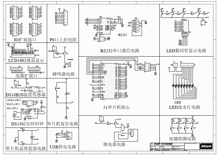
LCD1602液晶显示
J5 VCC J6 GND GND 1 2 3 4 5 6 7 8 1 2 3 4 5 6 7 8 VCC GND
Speaker
电源扩展口
VCC JP6 R1 4.7K TEMP P21 GND 2 1 DQ GND VCC 3 DS1820 VCC 1 2
蜂鸣器电路
VCC VCC RESET
VCCC7 C10 T1OUT R1IN GND 1 6 2 7 3 8 4 9 5
COM DISPLAY 11 GND 10 P10 P11 P12 P13 P14 P15 P16 P17 11 7 4 2 1 10 5 3 A B C D E F G DP 2 1
VCC A SEG JP1
I钟 单片机复位电路
33pF C2 X2 VCC C5 4.7uF 1 2 3 4 U3 VCC DD+ GND USB供电 GND C3 X1 D Y1 11.0592MHZ GND 33pF
K1
GND KEY1 P7 1 2 3 OUT KEY2 KEY3 KEY4
RELAY
D
按键检测电路
Title
GND
单片机晶体震荡电路 USB供电电路
1 2 3 4
继电器电路
5 6
多功能51单片机实验板
Number: Revision: V2.0
Designed By LiuJiahang
Size: A3
Date: 2009-6-5 Sheet 1 of 1 Time: 15:05:15 File: C:\Documents and Settings\heut\桌面\51实验板--刘佳杭\51.SchDoc 7 8
P37
基于P89LV51RD2单片机的温度控制处理系统的设计与实现

ElectronicComponent&DeviceApplicationsVol.10No.2Feb.2008第10卷第2期2008年2月0引言温度是一种最基本的环境参数。
人们日常生活与温度息息相关,工业生产中需要对温度进行监控,农业方面需要参考温度来进行生产,可见,温度在许多方面都起着重要的作用。
因此,对温度进行测量,并将数据进行存储,以备将来参考使用具有重要意义。
为此,本文将设计一个较为简易,成本较低,能实时监控并显示温度,使用方便的温度采集控制系统。
其中,温度的采集工作主要由温度传感器DS1820来完成,而采集到的温度数据则存于目前比较流行的SD卡中。
而控制与转换处理功能则采用新款单片机P89LV51RD2来实现,温度的显示由锁存器74LV377驱动三片数码管来实现。
本文首先介绍了控制处理系统设计的原理,接着给出了硬件的连接和系统的配置方法,最后介绍了软件程序的编写方法。
1温度控制处理系统设计图1给出了一个温度控制与处理系统的实现原理框图。
系统中的硬件主要包括温度传感器DS1820、单片机P89LV51RD2、SD卡、锁存器74LV77以及数码管。
系统工作时,先由温度传感器DS1820对温度进行测量,并将所测得的温度值转化成9位二进制数据后以串行方式传输到单片机P89LV51RD2,然后由单片机将收到的9位温度数据存到内部RAM中,并根据这个值来控制输出端口,同时将信息值送入对应的锁存器中,再由锁存器来驱动数码管,最后将温度值以摄氏温度的形式显示出来。
与此同时,系统在显示时不要将RAM中的数据以串行方式传入SD卡中进行存储,以便在需要时再将有用数据从卡读取出来。
下面就各芯片的工作模式与相关配置进行说明。
1.1数字温度传感器DS1820DS1820数字温度传感器的内部结构如图2所示。
由图可知,DS1820由三个主要数字器件组成:64bit闪速ROM、温度传感器、非易失性温度报警触发器TH和TL。
51学习板电路原理图

一体化红外接收头SM0038
D00 D01 D02 D03 D04 D05 D06 D07
IOUT1 11 IOUT2 12 GND 3 GND 10
D16
U15 D35 1 CS D37 2 RD D36 3 WR 5 INTR D17 11 DB7 D16 12 DB6 D15 13 DB5 D14 14 DB4 D13 15 DB3 D12 16 DB2 D11 17 DB1 D10 18 DB0 ADC0804
U12 1 D21 11 D00 D01 D02 D03 D04 D05 D06 D07 2 3 4 5 6 7 8 9 OC C 1D 2D 3D 4D 5D 6D 7D 8D 74HC573 1Q 2Q 3Q 4Q 5Q 6Q 7Q 8Q 19 18 17 16 15 14 13 12 X1 X2 X3 X4 X5 X6 X7 X8
20 19 18 17 16 15 14 13
1
2
3
4
5 Y7
1
2
3
4
5
6
Y5
Y4
Y8
Y3
X8
6
8 7 6 5 4 3 2 1
D07 D06 D05 D04 D03 D02
U8 1 D20 11 D00 D01 D02 D03 D04 D05 D06 D07 2 3 4 5 6 7 8 9 OC C 1D 2D 3D 4D 5D 6D 7D 8D 74HC573 1Q 2Q 3Q 4Q 5Q 6Q 7Q 8Q 19 18 17 16 15 14 13 12 Y1 Y2 Y3 Y4 Y5 Y6 Y7 Y8
J2 6 5 3 2
自锁按键
K5
K10
K15
p89v51rd2
P89V51RD28-bit 80C51 5V low power 64kB Flash microcontrollerwith 1kB RAMRev. 01 — 01 March 2004Product data 1.General descriptionThe P89V51RD2 is an 80C51 microcontroller with 64kB Flash and 1024 bytes ofdata RAM.A key feature of the P89V51RD2 is its X2 mode option. The design engineer canchoose to run the application with the conventional 80C51 clock rate (12clocks permachine cycle) or select the X2 mode (6clocks per machine cycle) to achieve twicethe throughput at the same clock frequency. Another way to benefit from this featureis to keep the same performance by reducing the clock frequency by half, thusdramatically reducing the EMI.The Flash program memory supports both parallel programming and in serialIn-System Programming(ISP).Parallel programming mode offers gang-programmingat high speed, reducing programming costs and time to market. ISP allows a deviceto be reprogrammed in the end product under software control. The capability tofield/update the application firmware makes a wide range of applications possible.The P89V51RD2 is also In-Application Programmable (IAP), allowing the Flashprogram memory to be reconfigured even while the application is running.2.Features80C51 Central Processing Unit5V Operating voltage from 0 to 40MHz64kB of on-chip Flash program memory with ISP (In-System Programming) andIAP (In-Application Programming)Supports 12-clock (default) or 6-clock mode selection via software or ISPSPI (Serial Peripheral Interface) and enhanced UARTPCA (Programmable Counter Array) with PWM and Capture/Compare functionsFour 8-bit I/O ports with three high-current Port 1 pins (16 mA each)Three 16-bit timers/countersProgrammable Watchdog timer (WDT)Eight interrupt sources with four priority levelsSecond DPTR registerLow EMI mode (ALE inhibit)TTL- and CMOS-compatible logic levelsBrown-out detectionLow power modesPower-down mode with external interrupt wake-upIdle modePDIP40, PLCC44 and TQFP44 packages3.Ordering informationTable 1:Ordering informationType number Package VersionName DescriptionP89V51RD2FA PLCC44plastic leaded chip carrier; 44 leads SOT187-2P89V51RD2FBC TQFP44plastic thin quad flat package; 44 leads SOT376-1P89V51RD2BN PDIP40plastic dual in-line package; 40 leads SOT129-13.1Ordering optionsTable 2:Ordering optionsType number Temperature range FrequencyP89V51RD2FA40°C to+85°C0 to 40MHzP89V51RD2FBC40°C to+85°CP89V51RD2BN0°C to+70°C4.Block diagramFig 1.P89V51RD2 block diagram.HIGH PERFORMANCE80C51 CPU64 kB CODE FLASH 1 kB DA T A RAMPORT 3OSCILLA TORINTERNAL BUSCRYSTAL ORRESONA TOR002aaa506UARTSPITIMER 2PCAPROGRAMMABLE COUNTER ARRAYTIMER 0TIMER 1WA TCHDOG TIMERPORT 2PORT 1PORT 05.Pinning information5.1PinningFig 2.PLCC44 pin configuration.P89V51RD2FA002aaa8107 8 9 10 11 12 13 14 15 16 173938373635343332313029 181922122232425262728654321444342414P1.4/SS/CEX1P1.3/CEXP1.2/ECIP1.1/T2EXP1./T2NCVCCP./ADP.1/AD1P.2/AD2P.3/AD3WR/P3.6RD/P3.7XTAL2XTAL1VSSNCA8/P2.A9/P2.1A1/P2.2A11/P2.3A12/P2.4CEX2/MOSI/P1.5 CEX3/MISO/P1.6 CEX4/SCK/P1.7RSTRXD/P3.0NCTXD/P3.1INT0/P3.2INT1/P3.3T0/P3.4T1/P3.5P0.4/AD4 P0.5/AD5 P0.6/AD6 P0.7/AD7 EANCALE/PROG PSENP2.7/A15 P2.6/A14 P2.5/A13Fig 3.PDIP40 pin configuration.handbook, halfpageP 89V 51R D 2B N002aaa8111234567891011121314151617181920T2/P1.0T2EX/P1.1ECI/P1.2CEX0/P1.3CEX1/SS/P1.4CEX2/MOSI/P1.5CEX3/MISO/P1.6CEX4/SCK/P1.7RST RXD/P3.0TXD/P3.1INT0/P3.2INT1/P3.3T0/P3.4T1/P3.5WR/P3.6RD/P3.7XTAL2XTAL1V SS V DD P0.0/AD0P0.1/AD1P0.2/AD2P0.3/AD3P0.4/AD4P0.5/AD5P0.6/AD6P0.7/AD7EA ALE/PROG PSEN P2.7/A15P2.6/A14P2.5/A13P2.4/A12P2.3/A11P2.2/A10P2.1/A9P2.0/A84039383736353433323130292827262524232221Fig 4.TQFP44 pin configuration.P89V51RD2FBC002aaa8121234567891011333231302928272625242312131415161718192021224443424140393837363534P 1.4/S S /C E X 1P 1.3/C E X 0P 1.2/E C IP 1.1/T 2E XP 1.0/T 2N CV D DP 0.0/A D 0P 0.1/A D 1P 0.2/A D 2P 0.3/A D 3W R /P 3.6R D /P 3.7X T A L 2X T A L 1V S S N C A 8/P 2.0A 9/P 2.1A 10/P 2.2A 11/P 2.3A 12/P 2.4CEX2/MOSI/P1.5CEX3/MISO/P1.6CEX4/SCK/P1.7RST RXD/P3.0NC TXD/P3.1INT0/P3.2INT1/P3.3T0/P3.4T1/P3.5P0.4/AD4P0.5/AD5P0.6/AD6P0.7/AD7EANC ALE/PROG PSEN P2.7/A15P2.6/A14P2.5/A135.2Pin descriptionTable 3:P89V51RD2 pin descriptionSymbol Pin Type Description DIP40TQFP44PLCC44P0.0 to P0.739-3237-3043-36I/O Port0:Port0 is an 8-bit open drain bi-directional I/Oport. Port0 pins that have ‘1’s written to them float, andin this state can be used as high-impedance inputs.Port0 is also the multiplexed low-order address anddata bus during accesses to external code and datamemory. In this application, it uses strong internalpull-ups when transitioning to ‘1’s. Port0 also receivesthe code bytes during the external host modeprogramming, and outputs the code bytes during theexternal host mode verification. External pull-ups arerequired during program verification or as a generalpurpose I/O port.P1.0 to P1.71-840-44, 1-32-9I/O withinternal pull-upPort1:Port 1 is an 8-bit bi-directional I/O port withinternal pull-ups. The Port 1 pins are pulled high by theinternal pull-ups when ‘1’s are written to them and canbe used as inputs in this state.As inputs,Port1pins thatare externally pulled LOW will source current (I IL)because of the internal pull-ups. P1.5, P1.6, P1.7 havehigh current drive of 16 mA. Port1 also receives thelow-order address bytes during the external host modeprogramming and verification.P1.01402I/O T2:External count input to Timer/Counter2or Clock-outfrom Timer/Counter 2P1.12413I T2EX: Timer/Counter 2 capture/reload trigger anddirection controlP1.23424I ECI: External clock input. This signal is the externalclock input for the PCA.P1.34435I/O CEX0:Capture/compare external I/O for PCA Module0.Each capture/compare module connects to a Port 1 pinfor external I/O.When not used by the PCA,this pin canhandle standard I/O.P1.45446I/O SS: Slave port select input for SPICEX1: Capture/compare external I/O for PCA Module1 P1.5617I/O MOSI: Master Output Slave Input for SPICEX2: Capture/compare external I/O for PCA Module2 P1.6728I/O MISO: Master Input Slave Output for SPICEX3: Capture/compare external I/O for PCA Module3 P1.7839I/O SCK: Master Output Slave Input for SPICEX4: Capture/compare external I/O for PCA Module4P2.0 to P2.721-2818-2524-31I/Owith internal pull-upPort 2: Port 2 is an 8-bit bi-directional I/O port with internal pull-ups. Port 2 pins are pulled HIGH by the internal pull-ups when ‘1’s are written to them and can be used as inputs in this state.As inputs,Port 2pins that are externally pulled LOW will source current (I IL )because of the internal pull-ups. Port 2 sends the high-order address byte during fetches from external program memory and during accesses to external Data Memory that use 16-bit address (MOVX@DPTR).In this application, it uses strong internal pull-ups whentransitioning to ‘1’s. Port 2 also receives some control signals and a partial of high-order address bits during the external host mode programming and verification.P3.0 to P3.710-175, 7-1311, 13-19I/Owith internal pull-upPort 3: Port 3 is an 8-bit bidirectional I/O port with internal pull-ups. Port 3 pins are pulled HIGH by the internal pull-ups when ‘1’s are written to them and can be used as inputs in this state.As inputs,Port 3pins that are externally pulled LOW will source current (I IL )because of the internal pull-ups. Port 3 also receives some control signals and a partial of high-order address bits during the external host mode programming and verification.P3.010511I RXD : serial input port P3.111713O TXD : serial output port P3.212814I INT0: external interrupt 0 input P3.313915I INT1: external interrupt 1 inputP3.4141016I T0: external count input to Timer/Counter 0P3.5151117I T1: external count input to Timer/Counter 1P3.6161218O WR : external data memory write strobe P3.7171319O RD : external data memory read strobePSEN292632I/OProgram Store Enable :PSEN is the read strobe for external program memory.When the device is executing from internal program memory,PSEN is inactive (HIGH). When the device is executing code fromexternal program memory,PSEN is activated twice each machine cycle, except that two PSEN activations are skipped during each access to external data memory.A forced HIGH-to-LOW input transition on the PSEN pin while the RST input is continually held HIGH for more than 10 machine cycles will cause the device to enter external host mode programming.RST 9410IReset :While the oscillator is running,a HIGH logic state on this pin for two machine cycles will reset the device.If the PSEN pin is driven by a HIGH-to-LOW input transition while the RST input pin is held HIGH, the device will enter the external host mode, otherwise the device will enter the normal operation mode.Table 3:P89V51RD2 pin description …continued Symbol Pin TypeDescriptionDIP40TQFP44PLCC44[1]ALE loading issue:When ALE pin experiences higher loading (>30pF)during the reset,the microcontroller may accidentally enter into modes other than normal working mode. The solution is to add a pull-up resistor of 3k to 50k to V DD , e.g., for ALE pin.[2]For 6-clock mode, ALE is emitted at 13 of crystal frequency.EA312935IExternal Access Enable :EA must be connected to V SS in order to enable the device to fetch code from the external program memory.EA must be strapped to V DD for internal program execution. However, Security lock level 4 will disable EA, and program execution is only possible from internal program memory.The EA pin can tolerate a high voltage of 12V .ALE/PROG302733I/OAddress Latch Enable: ALE is the output signal for latching the low byte of the address during an access to external memory. This pin is also the programmingpulse input (PROG)for flash programming.Normally the ALE [1] is emitted at a constant rate of 16 the crystal frequency [2] and can be used for external timing and clocking.One ALE pulse is skipped during each access to external data memory. However, if AO is set to ‘1’,ALE is disabled.NC -6, 17, 28,391, 12, 23,34I/O No ConnectXT AL1191521I Crystal 1: Input to the inverting oscillator amplifier and input to the internal clock generator circuits.XT AL2181420O Crystal 2: Output from the inverting oscillator amplifier.V DD 403844I Power supply V SS201622IGroundTable 3:P89V51RD2 pin description …continued Symbol Pin TypeDescriptionDIP40TQFP44PLCC446.Special function registersRemark:Special Function Registers (SFRs) accesses are restricted in the followingways:•User must not attempt to access any SFR locations not defined.•Accesses to any defined SFR locations must be strictly for the functions for theSFRs.•SFR bits labeled ‘-’, ‘0’ or ‘1’ can only be written and read as follows:–‘-’Unless otherwise specified,must be written with‘0’,but can return any valuewhen read(even if it was written with‘0’).It is a reserved bit and may be used infuture derivatives.–‘0’must be written with ‘0’, and will return a ‘0’ when read.–‘1’must be written with ‘1’, and will return a ‘1’ when read.Philips SemiconductorsP89V51RD28-bit microcontrollers with 80C51 core9397 750 12964© Koninklijke Philips Electronics N.V . 2004. All rights reserved.Product data Rev. 01 — 01 March 200411 of 75Table 4:Special function registers * indicates SFRs that are bit DescriptionSFR addr.Bit functions and addressesMSB LSB Bit addressE7E6E5E4E3E2E1E0ACC*AccumulatorE0H AUXR Auxiliary function register 8EH ------EXTRAMAO AUXR1Auxiliary function register 1A2H ---GF20-DPS Bit addressF7F6F5F4F3F2F1F0B* B registerF0H CCAP0H Module 0 Capture HIGH FAH CCAP1H Module 1 Capture HIGH FBH CCAP2H Module 2 Capture HIGH FCH CCAP3H Module 3 Capture HIGH FDH CCAP4H Module 4 Capture HIGH FEH CCAP0L Module 0 Capture LOW EAH CCAP1L Module 1 Capture LOW EBH CCAP2L Module 2 Capture LOW ECH CCAP3L Module 3 Capture LOW EDH CCAP4L Module 4 Capture LOW EEH CCAPM0Module 0 Mode DAH -ECOM_0CAPP_0CAPN_0MA T_0TOG_0PWM_0ECCF_0CCAPM1Module 1 Mode DBH -ECOM_1CAPP_1CAPN_1MA T_1TOG_1PWM_1ECCF_1CCAPM2Module 2 Mode DCH -ECOM_2CAPP_2CAPN_2MA T_2TOG_2PWM_2ECCF_2CCAPM3Module 3 Mode DDH -ECOM_3CAPP_3CAPN_3MA T_3TOG_3PWM_3ECCF_3CCAPM4Module 4 Mode DEH -ECOM_4CAPP_4CAPN_4MA T_4TOG_4PWM_4ECCF_4Bit addressDF DE DD DC DB DA D9D8CCON*PCA Counter Control D8H CFCR-CCF4CCF3CCF2CCF1CCF0CH PCA Counter HIGH F9H CL PCA Counter LOW E9H CMOD PCA Counter Mode D9HCIDLWDTE---CPS1CPS0ECFDPTR Data Pointer (2 bytes)DPH Data Pointer HIGH 83H DPLData Pointer LOW82HRev. 01 — 01 March 2004 12 of 75Bit address BF BE BD BC BB BA B9B8 IP0*Interrupt Priority B8H-PPC PT2PS PT1PX1PT0PX0IP0H Interrupt Priority 0 HIGH B7H-PPCH PT2H PSH PT1H PX1H PT0H PX0HBit address FF FE FD FC FB FA F9F8 IP1*Interrupt Priority 1F8H----PBOIP1H Interrupt Priority 1 HIGH F7H----PBOHFCF B1H-------BSELBit address8786858483828180 P0*Port080H AD7AD6AD5AD4AD3AD2AD1AD0Bit address9796959493929190 P1*Port 190H CEX4/SPICLKCEX3/MISOCEX2/MOSICEX1/SS CEX0ECI T2EX T2Bit address A7A6A5A4A3A2A1A0 P2*Port 2A0H A15A14A13A12A11A10A9A8Bit address B7B6B5B4B3B2B1B0 P3*Port 3B0H RD WR T1T0INT1INT0TxD RxDPCON Power Control Register87H SMOD1SMOD0BOF POF GF1GF0PD IDLBit address D7D6D5D4D3D2D1D0 PSW*Program Status Word D0H CY AC F0RS1RS0OV F1PRCAP2H Timer2 Capture HIGH CBHRCAP2L Timer2 Capture LOW CAHBit address9F9E9D9C9B9A9998 SCON*Serial Port Control98H SM0/FE_SM1SM2REN TB8RB8TI RISBUF Serial Port Data Buffer Register99HP89V51RD28-bit microcontrollers with 80C51 core © Koninklijke Philips Electronics N.V. 2004. All rights reserved.Rev. 01 — 01 March 200413 of 75[1]Unimplemented bits in SFRs (labeled’-’) are ‘X’s (unknown) at all times. Unless otherwise specified, ‘1’s should not be written to these bits since they may be used for otherpurposes in future derivatives. The reset values shown for these bits are‘0’s although they are unknown when read.SPDA T SPI Data86HSP Stack Pointer81HBit address8F8E8D8C8B8A8988 TCON*Timer Control Register88H TF1TR1TF0TR0IE1IT1IE0IT0Bit address CF CE CD CC CB CA C9C8 T2CON*Timer2 Control Register C8H TF2EXF2RCLK TCLK EXEN2TR2C/T2CP/RL2T2MOD Timer2 Mode Control C9H--ENT2T2OE DCENTH0Timer 0 HIGH8CHTH1Timer 1 HIGH8DHTH2Timer 2 HIGH CDHTL0Timer 0 LOW8AHTL1Timer 1 LOW8BHTL2Timer 2 LOW CCHTMOD Timer 0 and 1 Mode89H GATE C/T M1M0GA TE C/T M1M0WDTC Watchdog Timer Control C0H---WDOUT WDRE WDTS WDT SWDTWDTD Watchdog Timer Data/Reload85HP89V51RD28-bit microcontrollers with 80C51 core © Koninklijke Philips Electronics N.V. 2004. All rights reserved.8-bit microcontrollers with 80C51 core 7.Functional description7.1Memory organizationThe device has separate address spaces for program and data memory.7.1.1Flash program memoryThere are two internal flash memory blocks in the device. Block 0 has 64kbytes andcontains the user’s code. Block 1 contains the Philips-provided ISP/IAP routines andmay be enabled such that it overlays the first 8kbytes of the user code memory.The 64kB Block 0 is organized as 512 sectors, each sector consists of 128 bytes.Access to the IAP routines may be enabled by clearing the BSEL bit in the FCFregister. However, caution must be taken when dynamically changing the BSEL bit.Since this will cause different physical memory to be mapped to the logical programaddress space, the user must avoid clearing the BSEL bit when executing user codewithin the address range 0000H to 1FFFH.7.1.2Data RAM memoryThe data RAM has1024bytes of internal memory.The device can also address up to64kB for external data memory.7.1.3Expanded data RAM addressingThe P89V51RD2has1kB of RAM.See Figure5“Internal and external data memorystructure.” on page 17.The device has four sections of internal data memory:1.The lower128bytes of RAM(00H to7FH)are directly and indirectly addressable.2.The higher 128bytes of RAM (80H to FFH) are indirectly addressable.3.The special function registers (80H to FFH) are directly addressable only.4.The expanded RAM of 768bytes (00H to 2FFH) is indirectly addressable by themove external instruction (MOVX) and clearing the EXTRAM bit. (See ‘AuxiliaryRegister (AUXR) in Section 6 “Special function registers” on page 10)Since the upper 128bytes occupy the same addresses as the SFRs, the RAM mustbe accessed indirectly. The RAM and SFRs space are physically separate eventhough they have the same addresses.Table 5:AUXR - Auxiliary register (address 8EH) bit allocationNot bit addressable; Reset value 00HBit76543210Symbol------EXTRAM AO8-bit microcontrollers with 80C51 coreTable 6:AUXR - Auxiliary register (address 8EH) bit descriptionBit Symbol Description7 to 2-Reserved for future use. Should be set to ‘0’ by user programs.1EXTRAM Internal/External RAM access using MOVX @Ri/@DPTR.When ‘0’, core attempts to access internal XRAM with addressspecified in MOVX instruction. If address supplied with thisinstruction exceeds on-chip available XRAM, off-chip XRAM isgoing to be selected and accessed.When ‘1’, every MOVX @Ri/@DPTR instruction targets externaldata memory by default.0AO ALE off: disables/enables ALE. AO=0 results in ALE emitted at aconstant rate of12the oscillator frequency.In case of AO=1,ALEis active only during a MOVX or MOVC.When instructions access addresses in the upper 128 bytes (above 7FH), the MCU determines whether to access the SFRs or RAM by the type of instruction given. If it is indirect, then RAM is accessed. If it is direct, then an SFR is accessed. See the examples below.Indirect Access:MOV@R0, #data; R0 contains 90HRegister R0 points to 90H which is located in the upper address range. Data in‘#data’ is written to RAM location 90H rather than port 1.Direct Access:MOV90H, #data; write data to P1Data in ‘#data’ is written to port 1. Instructions that write directly to the address write to the SFRs.To access the expanded RAM, the EXTRAM bit must be cleared and MOVX instructions must be used.The extra768bytes of memory is physically located on the chip and logically occupies thefirst768bytes of external memory(addresses000H to 2FFH).When EXTRAM=0, the expanded RAM is indirectly addressed using the MOVX instruction in combination with any of the registers R0, R1 of the selected bank or DPTR. Accessing the expanded RAM does not affect ports P0, P3.6 (WR), P3.7 (RD), or P2. With EXTRAM=0, the expanded RAM can be accessed as in the following example.Expanded RAM Access (Indirect Addressing only):MOVX@DPTR, A DPTR contains 0A0HDPTR points to 0A0H and data in ‘A’ is written to address 0A0H of the expanded RAM rather than external memory. Access to external memory higher than 2FFH using the MOVX instruction will access external memory (0300H to FFFFH) and will perform in the same way as the standard8051,with P0and P2as data/address bus, and P3.6 and P3.7 as write and read timing signals.8-bit microcontrollers with 80C51 coreWhen EXTRAM =1, MOVX @Ri and MOVX @DPTR will be similar to the standard 8051. Using MOVX @Ri provides an 8-bit address with multiplexed data on Port 0.Other output port pins can be used to output higher order address bits.This provides external paging capabilities. Using MOVX @DPTR generates a 16-bit address. This allows external addressing up the 64kB.Port 2provides the high-order eight address bits (DPH), and Port 0 multiplexes the low order eight address bits (DPL) with data.Both MOVX @Ri and MOVX @DPTR generates the necessary read and writesignals (P3.6 -WR and P3.7 -RD) for external memory use.Table 7 shows external data memory RD,WR operation with EXTRAM bit.The stack pointer (SP)can be located anywhere within the 256bytes of internal RAM (lower 128 bytes and upper 128 bytes). The stack pointer may not be located in any part of the expanded RAM.[1]Access limited to ERAM address within 0 to 0FFH; cannot access 100H to 02FFH.Table 7:External data memory RD,WR with EXTRAM bitAUXRMOVX @DPTR, A or MOVX A,@DPTR MOVX @Ri, A or MOVX A, @Ri ADDR < 0300HADDR 0300HADDR =anyEXTRAM =0RD/WR not assertedRD/WR asserted RD/WR not assertedEXTRAM =1RD/WR asserted RD/WR asserted RD/WR asserted8-bit microcontrollers with 80C51 core7.1.4Dual data pointersThe device has two 16-bit data pointers. The DPTR Select (DPS) bit in AUXR1determines which of the two data pointers is accessed. When DPS =0, DPTR0 is selected;when DPS =1,DPTR1is selected.Quickly switching between the two data pointers can be accomplished by a single INC instruction on AUXR1 (see Figure 6).Fig 5.Internal and external data memory structure.000H2FFH00HFFHUPPER 128 BYTES INTERNAL RAM LOWER 128 BYTES INTERNAL RAM (INDIRECT & DIRECTADDRESSING)(INDIRECT ADDRESSING)(DIRECT ADDRESSING)SPECIAL FUNCTIONREGISTERS (SFRs)80HFFHFFFFH000HEXTERNAL DA T A MEMORYEXTERNAL DAT A MEMORY2FFH0000HEXTRAM = 0EXTRAM = 1EXP ANDED RAM0300H(INDIRECT ADDRESSING)(INDIRECT ADDRESSING)(INDIRECT ADDRESSING)FFFFH80H 7FH002aaa517EXP ANDEDRAM 768 BytesFig 6.Dual data pointer organization.DPL 82HDPS = 0 DPTR0DPS = 1 DPTR1external data memoryDPS002aaa518DPH 83HDPTR0DPTR1AUXR1 / bit08-bit microcontrollers with 80C51 core Table 8:AUXR1 - Auxiliary register 1 (address A2H) bit allocationNot bit addressable; Reset value 00HBit 76543210Symbol----GF20-DPSTable 9:AUXR1 - Auxiliary register 1 (address A2H) bit descriptionBit Symbol Description7 to 4-Reserved for future use. Should be set to ‘0’ by user programs.3GF2General purpose user-defined flag.20This bit contains a hard-wired‘0’.Allows toggling of the DPS bit byincrementing AUXR1, without interfering with other bits in theregister.1-Reserved for future use. Should be set to ‘0’ by user programs.0DPS Data pointer select. Chooses one of two Data Pointers for use bythe program. See text for details.7.2Flash memory In-Application Programming7.2.1Flash organizationThe P89V51RD2 program memory consists of a 64kB block. An In-SystemProgramming (ISP) capability, in a second 8kB block, is provided to allow the usercode to be programmed in-circuit through the serial port.There are three methods of erasing or programming of the Flash memory that may be used.First,the Flash may be programmed or erased in the end-user application by calling low-level routinesthrough a common entry point (IAP). Second, the on-chip ISP boot loader may beinvoked. This ISP boot loader will, in turn, call low-level routines through the samecommon entry point that can be used by the end-user application. Third, the Flashmay be programmed or erased using the parallel method by using a commerciallyavailable EPROM programmer which supports this device.7.2.2Boot blockWhen the microcontroller programs its own Flash memory, all of the low level details are handled by code that is contained in a Boot block that is separate from the user Flash memory. A user program calls the common entry point in the Boot block withappropriate parameters to accomplish the desired operation. Boot block operationsinclude erase user code, program user code, program security bits, etc.A Chip-Erase operation can be performed using a commercially available parallelprogramer. This operation will erase the contents of this Boot Block and it will benecessary for the user to reprogram this Boot Block (Block 1) with thePhilips-provided ISP/IAP code in order to use the ISP or IAP capabilities of thisdevice. Contact to obtain the hex file forthis device. Questions may be directed to micro.support@.8-bit microcontrollers with 80C51 core7.2.3Power-On reset code executionFollowing reset, the P89V51RD2 will either enter the SoftICE mode (if previouslyenabled via ISP command) or attempt to autobaud to the ISP boot loader. If thisautobaud is not successful within about400ms,the device will begin execution of the user code.7.2.4In-System Programming (ISP)In-System Programming is performed without removing the microcontroller from the system.The In-System Programming facility consists of a series of internal hardware resources coupled with internal firmware to facilitate remote programming of theP89V51RD2 through the serial port. This firmware is provided by Philips andembedded within each P89V51RD2 device. The Philips In-System Programmingfacility has made in-circuit programming in an embedded application possible with a minimum of additional expense in components and circuit board area. The ISPfunction usesfive pins(V DD,V SS,TxD,RxD,and RST).Only a small connector needs to be available to interface your application to an external circuit in order to use thisfeature.7.2.5Using the In-System ProgrammingThe ISP feature allows for a wide range of baud rates to be used in your application, independent of the oscillator frequency. It is also adaptable to a wide range ofoscillator frequencies. This is accomplished by measuring the bit-time of a single bit in a received character. This information is then used to program the baud rate interms of timer counts based on the oscillator frequency.The ISP feature requires that an initial character(an uppercase U)be sent to the P89V51RD2to establish the baud rate. The ISP firmware provides auto-echo of received characters. Once baud rateinitialization has been performed, the ISP firmware will only accept Intel Hex-typerecords.Intel Hex records consist of ASCII characters used to represent hexadecimal values and are summarized below::NNAAAARRDD..DDCC<crlf>In the Intel Hex record, the ‘NN’ represents the number of data bytes in the record.The P89V51RD2 will accept up to 32 data bytes. The ‘AAAA’ string represents theaddress of thefirst byte in the record.If there are zero bytes in the record,thisfield is often set to 0000. The ‘RR’ string indicates the record type. A record type of ‘00’ is a data record. A record type of ‘01’ indicates the end-of-file mark. In this application,additional record types will be added to indicate either commands or data for the ISP facility.The maximum number of data bytes in a record is limited to 32 (decimal). ISPcommands are summarized in T able10. As a record is received by the P89V51RD2, the information in the record is stored internally and a checksum calculation isperformed. The operation indicated by the record type is not performed until theentire record has been received. Should an error occur in the checksum, theP89V51RD2 will send an ‘X’ out the serial port indicating a checksum error. If thechecksum calculation is found to match the checksum in the record, then thecommand will be executed. In most cases, successful reception of the record will be indicated by transmitting a ‘.’ character out the serial port.。
跑马灯的设计与制作-林瑞柠
焊接电路
图 5 跑马灯部分(左),MAX 烧写器部分(中),两部分合成的电路板(右)
这是一个比较重要而且又难的部分,我们是分两个部分焊接的,单片机在一个板(如图 6),烧写器一个 板(如图 7),当然,我们还做了一个把两个都结合起来的电路板(如图 8)。 过程:
擦除完毕后,点击图 9 中的“Start”按钮,就可以将代码下载到芯片中,下载完毕后,如图 12 会变为
如图 13 所示,然后按复位键就可以动程程序。
在使用 Flash Magic 过程中,经常会弹出图 10 所示的对话框提示系统没有进 ISP 模式,这时只要按一下
硬件电路的复位键或重新上电即可。
程序原代码
总体性检测
这是最后的工作,电路焊好后不一定就正确了,这时用 万用表来检测电路是否有可能短路,或是正负极接错了等。 有错则就改正过来,最好多检测几次(其实在焊接过程也应 部分的检测)。
3 跑马灯的调试
图 6 Flash Magic 主界面 图 7 未进入 ISP 的错误提示
烧写软件——Flash Magic
/* 该实验是流水灯(8 个发光二极管循环点亮),功能是流水灯(8 个发光二极管循环以 1S 间隔点亮) */
#include<reg52.h>//包含 reg.52 文件 #include<intrins.h>//包含左右循环移位子函数库文件 #define uint unsigned int//宏定义
Flash Magic 是 Philips 提供的一个把原程序嵌入到单片 机里的软件,如何在 Device 中找不到 P89V52RD2 单片机, 说明 Flash Magic 的版本过旧,所以最好是下载一个新的版 本。
基于P89V51RD2的多功能蓄电池充电系统设计
基于P89V51RD2的多功能蓄电池充电系统设计免维护蓄电池(简称蓄电池)以易用、价廉和储能比高等优良性能在电动自行车、电动游览车及不间断电源系统中得到广泛的应用,成为普及率最高的电能储能设备。
目前的蓄电池充电器绝大多数以恒流恒压方式充电,没有考虑环境温度变化对蓄电池充电过程的影响,影响了蓄电池性能的充分发挥和使用寿命。
笔者结合蓄电池的充电特性,以P89V51RD2型微处理器为控制核心,开发了多功能数字式蓄电池充电机,实现了对36 V以下、100 Ah以内的蓄电池的初充、激活、快充和正常充电等功能,同时根据环境温度变化,自动调整充电终止电压,实现了充电过程的智能化。
2 蓄电池充电特性蓄电池的充电是一个复杂的电化学过程。
影响充电效果的因素很多,温度即是其中之一。
图1所示是以新的12 V/100 Ah蓄电池为对象,以0.1 CA(CA为蓄电池的标定容量,单位为A·h)的标准恒定电流在不同环境温度下的充电特性曲线。
由图1可以看出,在充电过程中,温度的改变会对充电电压产生重要影响。
温度在O℃~5℃时,其充电端电压会上升约2%,在10℃~25℃时充电端电压上升约1.5%,而在35℃~40℃时充电端电压下降约1%;当温度高于55℃时充电端电压下降5%。
由此可见,采用恒压充电模式,在冬季充电可能不足,而在夏季蓄电池可能过充电。
实践也证明,蓄电池在充电过程中电压随时间呈指数规律下降,即使是相同型号、相同容量的蓄电池,因放电状态、使用和保存期的不同,其充电性能也大不一样。
因此,不可能按恒流或恒压进行充电。
3 主要元器件TLC2543是11通道高速A/D转换器,采样速率达200 kHz,其输入命令格式如表1所示,工作时序如图2所示。
OCM2X8C是:128x32点阵液晶显示模块,可显示汉字及图形,内置8192个汉字(16x16点阵)、128个字符(8x16点阵)。
可与CPU直接接口,提供8位并行及串行连接方式,具有多种功能光标显示、画面移位、睡眠模式等功能。
如何使用P89V51RD2单片机
如何使用P89V51RD2单片机P89V51RD2器件含有2个内部Flash存储模块,可实现对器件在系统编程(ISP)和在应用中编程(IAP)。
模块0有64K字节,用来存放用户代码;模块1有8K字节,用来存放Philips提供的ISP/IAP程序,在出厂时,该程序已被固化到模块1中。
在使用P89V51RD2时,只需要将用户代码写入模块0中即可。
写入的方法有两种:1)用通用编程器将用户程序烧写到单片机中;2)使用芯片的ISP功能配合下载软件将程序下载到芯片中。
以下将重点讲述P89V51RD2这两种写入方法,并简单的介绍它的IAP功能。
1. 在系统编程(ISP)使用方法ISP功能是指用户在编程时不需要将微控制器从系统中移出。
在系统编程特性包含了一系列内部的硬件资源,与内部固件的结合可实现通过串口对P89V51RD2的远程编程。
固件由PHILIPS提供并嵌入到每一个芯片当中。
ISP功能使用芯片的5个管脚(Vdd、Vss、TxD、RxD、RST),只需要一个小的连接器就可实现通过外部电路使用该特性的应用接口。
用户在搭建硬件电路时,需要引出串口以便和PC机通信。
在搭建好硬件电路后,将串口和PC机相连,上电后就可使用ISP功能下载程序了。
使用P89V51RD2的ISP功能时,需要配合下载软件Flash Magic一起使用。
运行Flash Magic,选择正确的串口、设置波特率、选择芯片P89V51RD2,设置的界面如图1所示。
如果在“Device”中找不到“P89V51RD2”单片机,说明Flash Magic的版本过旧,需要下载一个新的版本,安装后即可使用。
下载网址为:/software/flashmagic/图1 Flash Magic界面设置以上操作完成后,关闭Flash Magic,重新启动。
这时会弹出如图2所示的界面,提示用户未进入ISP。
这时只需按一下硬件电路的复位键或重新上电即可。
图2 未进ISP模式的错误提示P89V51RD2进入ISP模式后,就可以下载用户程序到单片机的Flash区了。