飞思卡尔芯片简介
飞思卡尔高功率器件介绍
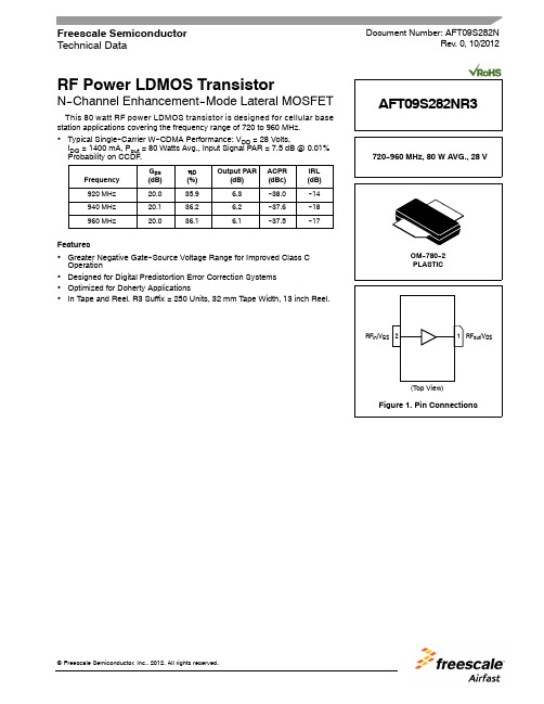
RF Power LDMOS TransistorN--Channel Enhancement--Mode Lateral MOSFETThis 80watt RF power LDMOS transistor is designed for cellular base station applications covering the frequency range of 720to 960MHz.•Typical Single--Carrier W--CDMA Performance:V DD =28Volts,I DQ =1400mA,P out =80Watts Avg.,Input Signal PAR =7.5dB @0.01%Probability on CCDF.Frequency G ps (dB)ηD (%)Output PAR(dB)ACPR (dBc)IRL (dB)920MHz 20.035.9 6.3--38.0--14940MHz 20.136.2 6.2--37.6--18960MHz20.036.16.1--37.5--17Features•Greater Negative Gate--Source Voltage Range for Improved Class C Operation•Designed for Digital Predistortion Error Correction Systems •Optimized for Doherty Applications•In Tape and Reel.R3Suffix =250Units,32mm Tape Width,13inch Reel.Document Number:AFT09S282NRev.0,10/2012Technical Data720--960MHz,80W AVG.,28VAFT09S282NR3AFT09S282NR3Table 1.Maximum RatingsRatingSymbol Value Unit Drain--Source Voltage V DSS --0.5,+70Vdc Gate--Source Voltage V GS --6.0,+10Vdc Operating VoltageV DD 32,+0Vdc Storage Temperature Range T stg --65to +150°C Case Operating Temperature Range T C --40to +150°C Operating Junction Temperature Range (1,2)T J--40to +225°CTable 2.Thermal CharacteristicsCharacteristicSymbol Value (2,3)Unit Thermal Resistance,Junction to CaseCase Temperature 80°C,80W CW,28Vdc,I DQ =1500mA,960MHz Case Temperature 91°C,282W CW,28Vdc,I DQ =1500mA,960MHzR θJC0.310.27°C/WTable 3.ESD Protection CharacteristicsTest MethodologyClass Human Body Model (per JESD22--A114)2Machine Model (per EIA/JESD22--A115)B Charge Device Model (per JESD22--C101)IVTable 4.Moisture Sensitivity LevelTest MethodologyRating Package Peak TemperatureUnit Per JESD22--A113,IPC/JEDEC J--STD--0203260°CTable 5.Electrical Characteristics (T A =25°C unless otherwise noted)CharacteristicSymbolMinTypMaxUnitOff CharacteristicsZero Gate Voltage Drain Leakage Current (V DS =70Vdc,V GS =0Vdc)I DSS ——10μAdc Zero Gate Voltage Drain Leakage Current (V DS =28Vdc,V GS =0Vdc)I DSS ——1μAdc Gate--Source Leakage Current (V GS =5Vdc,V DS =0Vdc)I GSS——1μAdcOn CharacteristicsGate Threshold Voltage(V DS =10Vdc,I D =370μAdc)V GS(th) 1.0 1.5 2.0Vdc Gate Quiescent Voltage(V DD =28Vdc,I D =1400mA,Measured in Functional Test)V GS(Q) 1.7 2.2 2.7Vdc Drain--Source On--Voltage(V GS =10Vdc,I D =3.6Adc)V DS(on)0.10.140.3Vdc1.Continuous use at maximum temperature will affect MTTF.2.MTTF calculator available at /rf.Select Software &Tools/Development Tools/Calculators to access MTTF calculators by product.3.Refer to AN1955,Thermal Measurement Methodology of RF Power Amplifiers.Go to /rf.Select Documentation/Application Notes --AN1955.(continued)AFT09S282NR3Table 5.Electrical Characteristics (T A =25°C unless otherwise noted)(continued)CharacteristicSymbolMinTypMaxUnitFunctional Tests (1)(In Freescale Test Fixture,50ohm system)V DD =28Vdc,I DQ =1400mA,P out =80W Avg.,f =960MHz,Single--Carrier W--CDMA,IQ Magnitude Clipping,Input Signal PAR =7.5dB @0.01%Probability on CCDF.ACPR measured in 3.84MHz Channel Bandwidth @±5MHz Offset.Power Gain G ps 19.020.022.0dB Drain EfficiencyηD 33.536.1—%Output Peak--to--Average Ratio @0.01%Probability on CCDF PAR 5.6 6.1—dB Adjacent Channel Power Ratio ACPR —--37.5--36.0dBc Input Return LossIRL—--17--10dBLoad Mismatch (In Freescale Test Fixture,50ohm system)I DQ =1400mA,f =940MHzVSWR 10:1at 32Vdc,416W CW Output Power(3dB Input Overdrive from 280W CW Rated Power)No Device DegradationTypical Performance (In Freescale Test Fixture,50ohm system)V DD =28Vdc,I DQ =1400mA,920--960MHz Bandwidth P out @1dB Compression Point,CWP1dB —280—W VBW Resonance Point(IMD Third Order Intermodulation Inflection Point)VBW res —60—MHz Gain Flatness in 40MHz Bandwidth @P out =80W Avg.G F —0.1—dB Gain Variation over Temperature (--30°C to +85°C)∆G —0.0156—dB/°C Output Power Variation over Temperature (--30°C to +85°C)∆P1dB—0.006—dB/°C1.Part internally matched both on input and output.AFT09S282NR3Figure2.AFT09S282NR3Test Circuit Component Layout*C26is mounted vertically.Table6.AFT09S282NR3Test Circuit Component Designations and ValuesPart Description Part Number Manufacturer C162pF Chip Capacitor ATC100B620JT500XT ATCC2,C5,C10,C13 4.7pF Chip Capacitors ATC600F4R7BT250XT ATCC3,C7,C14,C15,C22,C2310μF Chip Capacitors GRM32ER71H106KA12L MurataC4,C6,C16,C17,C18,C1947pF Chip Capacitors ATC600F470JT250XT ATCC8,C9,C11,C24 3.9pF Chip Capacitors ATC600F3R9BT250XT ATCC12,C20,C21 2.4pF Chip Capacitors ATC600F2R4BT250XT ATCC25470μF,63V Electrolytic Capacitor MCGPR63V477M13X26-RH MulticompC2636pF Chip Capacitor ATC100B360JT500XT ATCR1,R2 6.04Ω,1/4W Chip Resistor CRCW12066R04FKEA VishayPCB0.020″,εr=3.5RO4350RogersAFT09S282NR3TYPICAL CHARACTERISTICSI R L ,I N P U T R E T U R N L O S S (d B )820f,FREQUENCY (MHz)Figure 3.Single--Carrier Output Peak--to--Average Ratio Compression(PARC)Broadband Performance @P out =80Watts Avg.--20--0--5--10--1513232221--4238343026--37--38--39--40ηD ,D R A I N E F F I C I E N C Y (%)G p s ,P O W E R G A I N (d B )20191817161584086088090092094096098022--41--25A C P R (dB c )Figure 4.Intermodulation Distortion Productsversus Two--Tone SpacingTWO--TONE SPACING (MHz)10-----1100I M D ,I N T E R M O D U L A T I O N D I S T O R T I O N (d B c )-Figure 5.Output Peak--to--Average RatioCompression (PARC)versus Output PowerP out ,OUTPUT POWER (WATTS)--1--3700--2--4O U T P U T C O M P R E S S I O N A T 0.01%P R O B A B I L I T Y O N C C D F (d B )509011015020504540353025ηD ,D R A I N E F F I C I E N C Y (%)130A C P R (dB c )--50--20--25--30--40--35--4522G p s ,P O W E R G A I N (d B )212019181716P A R C (d B )--1.8--1--1.2--1.4--1.6--2--51AFT09S282NR3TYPICAL CHARACTERISTICS1P out,OUTPUT POWER(WATTS)AVG.Figure6.Single--Carrier W--CDMA Power Gain,DrainEfficiency and ACPR versus Output Power--10--20 16226050403020ηD,DRAINEFFICIENCY(%)Gps,POWERGAIN(dB)21201010030010--60ACPR(dBc) 191817--30--40--50 Figure7.Broadband Frequency Response1123f,FREQUENCY(MHz)191715GAIN(dB)2113700800900100011001200130014001500--402010--10--20IRL(dB)--30AFT09S282NR3V DD =28Vdc,I DQ =1400mA ,Pulsed CW,10μsec(on),10%Duty Cyclef (MHz)Z source (Ω)Z in (Ω)Z load (1)(Ω)Max Linear Gain (dB)Max Output PowerP1dBP3dB(dBm)(W)ηD(%)AM/PM (°)(dBm)(W)ηD (%)AM/PM (°)920 1.83-j3.18 1.66+j3.17 4.55-j3.2718.756.039653.5-8.056.949458.2-12940 2.01-j3.27 2.03+j3.31 4.97-j2.8618.755.939154.4-7.756.949057.6-119602.64-j3.342.55+j3.455.77-j1.7818.455.939153.9-7.956.948857.8-12(1)Load impedance for optimum P1dB power.Z source =Measured impedance presented to the input of the device at the package reference plane.Z in =Impedance as measured from gate contact to ground.Z load =Measured impedance presented to the output of the device at the package reference plane.source inloadFigure 8.Load Pull Performance —Maximum P1dB TuningV DD =28Vdc,I DQ =1400mA ,Pulsed CW,10μsec(on),10%Duty Cyclef (MHz)Z source (Ω)Z in (Ω)Z load (1)(Ω)Max Linear Gain (dB)Max Drain EfficiencyP1dBP3dB(dBm)(W)ηD(%)AM/PM (°)(dBm)(W)ηD (%)AM/PM (°)920 1.83-j3.18 1.70+j3.02 1.49-j1.6122.053.522566.2-1554.326769.6-22940 2.01-j3.27 2.12+j3.16 1.48-j1.8022.053.321566.6-1654.024870.1-249602.64-j3.342.66+j3.261.76-j1.7921.753.623067.4-1554.326970.6-22(1)Load impedance for optimum P1dB efficiency.Z source =Measured impedance presented to the input of the device at the package reference plane.Z in =Impedance as measured from gate contact to ground.Z load =Measured impedance presented to the output of the device at the package reference plane.source inloadFigure 9.Load Pull Performance —Maximum Drain Efficiency TuningAFT09S282NR3P1dB --TYPICAL LOAD PULL CONTOURS —940MHz34567213456721--4.50--0.5--1.5--1--2--2.5--3.5--4--3--4.50--0.5--1.5--1--2--2.5--3.5--4--3--4.50--0.5--1.5--1--2--2.5--3.5--4--3I M A G I N A R Y (Ω)I M A G I N A R Y (Ω)NOTE:=Maximum Output Power=Maximum DrainEfficiencyFigure 10.P1dB Load Pull Output Power Contours (dBm)--4.5REAL (Ω)0--0.5--1.5I M A G I N A R Y (Ω)345Figure 11.P1dB Load Pull Efficiency Contours (%)REAL (Ω)I M A G I N A R Y (Ω)Figure 12.P1dB Load Pull Gain Contours (dB)REAL (Ω)Figure 13.P1dB Load Pull AM/PM Contours (°)REAL (Ω)--1--2--2.5--3.5--467--3213456721Power Gain Drain Efficiency LinearityOutput PowerAFT09S282NR3P3dB --TYPICAL LOAD PULL CONTOURS —940MHzNOTE:=Maximum Output Power =Maximum DrainEfficiencyFigure 14.P3dB Load Pull Output Power Contours (dBm)--41REAL (Ω)--1--2Figure 15.P3dB Load Pull Efficiency Contours (%)REAL (Ω)Figure 16.P3dB Load Pull Gain Contours (dB)REAL (Ω)Figure 17.P3dB Load Pull AM/PM Contours (°)REAL (Ω)Power Gain Drain Efficiency LinearityOutput Power--41--1--2014567--332I M A G I N A R Y (Ω)014567--332--41--1--2I M A G I N A R Y (Ω)014567--332--41--1--2I M A G I N A R Y (Ω)014567--332I M A G I N A R Y (Ω)AFT09S282NR3PACKAGEDIMENSIONSAFT09S282NR311RF Device Data Freescale Semiconductor,Inc.12RF Device Data Freescale Semiconductor,Inc.AFT09S282NR3AFT09S282NR313RF Device Data Freescale Semiconductor,Inc.PRODUCT DOCUMENTATION,SOFTWARE AND TOOLSRefer to the following documents,software and tools to aid your design process.Application Notes•AN1955:Thermal Measurement Methodology of RF Power AmplifiersEngineering Bulletins•EB212:Using Data Sheet Impedances for RF LDMOS DevicesSoftware•Electromigration MTTF Calculator•RF High Power Model•.s2p FileDevelopment Tools•Printed Circuit BoardsFor Software and Tools,do a Part Number search at ,and select the “Part Number”link.Go to the Software &Tools tab on the part’s Product Summary page to download the respective tool.REVISION HISTORYThe following table summarizes revisions to this document.RevisionDate Description0Oct.2012•Initial Release of Data SheetRF Device Data Freescale Semiconductor,rmation in this document is provided solely to enable system and software implementers to use Freescale products.There are no express or implied copyright licenses granted hereunder to design or fabricate any integrated circuits based on the information in this document.Freescale reserves the right to make changes without further notice to any products herein.Freescale makes no warranty,representation,or guarantee regarding the suitability of its products for any particular purpose,nor does Freescale assume any liability arising out of the application or use of any product or circuit,and specifically disclaims any and all liability,including without limitation consequential or incidental damages.“Typical”parameters that may be provided in Freescale data sheets and/or specifications can and do vary in different applications,and actual performance may vary over time.All operating parameters,including “typicals,”must be validated for each customer application by customer’s technical experts.Freescale does not convey any license under its patent rights nor the rights of others.Freescale sells products pursuant to standard terms and conditions of sale,which can be found at the following address:/SalesTermsandConditions.Freescale,the Freescale logo,AltiVec,C--5,CodeTest,CodeWarrior,ColdFire,C--Ware,Energy Efficient Solutions logo,Kinetis,mobileGT,PowerQUICC,Processor Expert,QorIQ,Qorivva,StarCore,Symphony,and VortiQa are trademarks of Freescale Semiconductor,Inc.,Reg.U.S.Pat.&Tm.Off.Airfast,BeeKit,BeeStack,ColdFire+,CoreNet,Flexis,MagniV,MXC,Platform in a Package,QorIQ Qonverge,QUICC Engine,Ready Play,SafeAssure,SMARTMOS,TurboLink,Vybrid,and Xtrinsic are trademarks of Freescale Semiconductor,Inc.All other product or service names are the property of their respective owners.E 2012Freescale Semiconductor,Inc.How to Reach Us:Home Page: Web Support:/support。
著名芯片厂商标志和简介之1

著名芯片厂商标志和简介之1标 志 公 司 简 介美国仙童(飞兆),采用世界级 4、5、6-inch 硅片工艺生产逻辑、模拟、混 合信号 IC 和分立元件 美国国际整流器公司成立于 1947 年,是主要的全球功率半导体供应商。
我们的产品通过电能转换,为各种电源系统、电机传动系统及照明镇流器 提供能源。
美国安森美半导体主要拥有三类产品系列: 电源管理和标准模拟集成电路 (放大器、电压参考、接口和比较器);高性能逻辑电路(特殊应用产品、 通信集成电路、时钟、转换器和驱动器);以及包括了有源分立元件和 MOSFET 产品的标准半导体。
IXYS美国 IXYS(艾赛斯)公司是世界著名的半导体厂家,成立于 1983 年, 总 部设于美国加利福尼亚州(二极管、MOS 管等半导体工厂设于德国) ,其 产品包括 MOSFET、IGBT、 Thyristor、SCR、整流桥、二极管、DCB 块、功率模块等。
主要产品:功率模块、MOSFET、整流桥 法国意法半导体公司 SGS-THOMSON,国际著名半导体公司之一。
美国摩托罗拉半导体 Motorola Semiconductor Products Inc.,以数字逻辑器 件、 模拟和接口器件、 通信及功率器件、 各类微处理器、 存储器电路为主。
美国飞思卡尔半导体(原摩托罗拉半导体部)是全球领先的半导体公司。
这 家私营跨国公司总部位于德州奥斯汀,在全球 30 多个国家和地区拥有设 计、研发、制造和销售机构。
飞思卡尔是全球最大的半导体公司之一。
从 其前身———摩托罗拉半导体部算起, 飞思卡尔已有 50 多年的发展历史, 从摩托罗拉分拆出来后,飞思卡尔有了完全中立的市场地位, 美国 APT (先进功率技术)公司(现 Microsemi 公司)。
提供双极晶体管、 VDMOS 和 LDMOS 三大类产品。
APT 于 2005/10/1 被 Microsemi 公司并购, 因此,APT 公司已于 2006/05/01 正式纳入 Microsemi 公司体系运作。
进口网络安全芯片排名

进口网络安全芯片排名进口网络安全芯片是保护网络安全的重要组成部分,它可以用来防御网络攻击、保护用户数据的安全性以及保障网络通信的可靠性。
随着互联网的迅速发展,网络安全问题也日益凸显,进口网络安全芯片的需求量逐渐增加。
下面就来介绍一下目前市场上几款知名的进口网络安全芯片。
1. 飞思卡尔(Freescale)Kinetis K61飞思卡尔公司是一家专门从事半导体产品研发的公司,在网络安全芯片领域具有较高的知名度。
Kinetis K61是飞思卡尔公司开发的一款高性能网络安全芯片,它采用了ARM Cortex-M4内核,具有优秀的处理性能和低功耗特性。
该芯片还支持多种安全功能,例如数据加密和身份验证等,能够有效地保护网络通信的安全性。
2. 英特尔(Intel)SGX英特尔公司是全球领先的半导体芯片制造商,其安全芯片技术在网络安全领域也有着广泛的应用。
Intel SGX(Software Guard Extensions)是一种支持硬件加密的安全芯片技术,它可以将软件运行在受保护的内存区域中,防止恶意软件的攻击和数据泄露。
SGX是一种非常理想的网络安全解决方案,目前已经广泛应用在云计算、物联网等领域。
3. 英飞凌(Infineon)OPTIGA TPM英飞凌公司是一家专门从事半导体和系统解决方案研发的公司,其网络安全芯片产品在市场上具有较高的声誉。
OPTIGA TPM 是英飞凌公司开发的一款安全芯片,它采用了可信平台模块(Trusted Platform Module,TPM)标准,可以为计算机和物联网设备提供可靠的安全认证和数据保护。
OPTIGA TPM芯片具有高度的安全性和可靠性,被广泛应用在金融、电子政务等领域。
4. STMicroelectronics ST33STMicroelectronics是一家全球领先的半导体解决方案供应商,其网络安全芯片产品也在行业内享有良好的声誉。
ST33是STMicroelectronics公司开发的一款安全芯片,它采用了ARM® SecurCore® SC300内核,具有出色的运算性能和安全性能。
飞思卡尔芯片
飞思卡尔芯片飞思卡尔(Freescale)是一家拥有嵌入式半导体解决方案的全球领先制造商。
该公司的产品覆盖了自动驾驶汽车、智能手机、物联网以及工业自动化等领域。
飞思卡尔芯片是该公司的核心产品之一,下面将对其进行详细介绍。
飞思卡尔芯片是一种用于嵌入式系统的半导体芯片,具有高性能、低能耗的特点。
它可以运行复杂的应用程序,并提供丰富的外设接口,以满足各种设备的需求。
飞思卡尔芯片使用先进的制造工艺,具有较高的集成度和稳定性,同时还具有较低的功耗和散热性能。
飞思卡尔芯片提供了多种型号和系列,以满足不同应用场景的需求。
例如,i.MX系列是用于智能手机和平板电脑等移动设备的芯片,具有高性能、低功耗和丰富的多媒体功能。
QorIQ系列则是用于工业和网络设备的芯片,具有高性能、可靠性和安全性。
飞思卡尔芯片的应用范围非常广泛。
在汽车行业,它可以用于自动驾驶系统、车载娱乐系统和车身控制系统等。
在消费电子行业,它可以用于智能手机、平板电脑和智能家居设备等。
在工业自动化领域,它可以用于工业机器人、智能仓储系统和智能制造设备等。
与传统的微控制器相比,飞思卡尔芯片具有更强大的计算能力和更丰富的外设接口。
它可以支持更复杂的算法和应用程序,并且可以实现更高的系统集成度。
此外,飞思卡尔芯片还具有较低的功耗和散热性能,能够降低系统的能耗和散热压力。
飞思卡尔芯片还提供了丰富的软件和开发工具,以便开发人员快速开发和调试嵌入式系统。
它支持多种操作系统和开发环境,如Linux、Android和Microcontroller等。
同时,飞思卡尔芯片还提供了可靠的技术支持和培训,以帮助客户解决技术和应用问题。
总之,飞思卡尔芯片是一种用于嵌入式系统的半导体芯片,具有高性能、低能耗和丰富的外设接口。
它可以满足各种设备的需求,在多个行业具有广泛的应用前景。
随着物联网和智能制造技术的发展,飞思卡尔芯片将为各种智能设备的发展提供强大的支持。
hef40106bt芯片工作原理
hef40106bt芯片工作原理Hef40106bt芯片是一种六反相器化器,并且是由飞思卡尔公司(Freescale)制造的。
它由6个反相器组成,它们可以将输入信号从高电平转换为低电平,或从低电平转换为高电平。
hef40106bt芯片工作原理如下:1. 引脚功能:hef40106bt芯片一共有14个引脚,分别是VCC(正电源),GND(地),以及6个反相器输入引脚A1,A2,A3,A4,A5和A6;以及6个反相器输出引脚B1,B2,B3,B4,B5和B6。
2. 输入和输出特性:每个反相器都有一个输入和一个输出引脚。
当输入引脚接收到高电平时,输出引脚会变为低电平;当输入引脚接收到低电平时,输出引脚会变为高电平。
因此,hef40106bt芯片的主要功能是将输入信号进行反相处理。
3. 功能特点:每个反相器都具有相同的工作原理和特点。
当输入引脚接收到高电平时,输入端和反馈端之间的集电极结就会导通,输出引脚变为低电平,同时电容器开始充电。
当输入引脚接收到低电平时,反馈端和电源之间的集电极结导通,输出引脚变为高电平,电容器开始放电。
这种充电和放电的过程会导致输入信号的相反反馈。
4. 应用:hef40106bt芯片广泛应用于不同的电子电路中,尤其是在模拟信号处理和数字信号处理领域。
它可以用作振荡器、时钟发生器、信号放大器和滤波器等。
5. 注意事项:在使用hef40106bt芯片时需要注意以下几点:- 输入信号的幅值必须在芯片的供电范围之内,通常为0V到VCC之间。
- 要避免输入信号的幅值超过芯片的最大额定值,以防止芯片损坏。
- 输入和输出引脚之间应正确连接,以确保正确的信号传输。
- 在设计电路时,要合理选择适当的电容器和电阻器,以满足所需的工作条件和性能指标。
综上所述,hef40106bt芯片是一种用于信号反相处理的六反相器化器。
它通过充电和放电的过程将输入信号从高电平转换为低电平或从低电平转换为高电平。
在实际应用中,我们需要根据具体需求选择合适的输入信号幅值范围,正确连接引脚,并合理设计电路,以确保芯片的正常工作和性能。
飞思卡尔8位单片机—飞思卡尔8位单片机基础知识

7〉 管脚的复用
注意: 0、管脚功能复用时的优先 级见右表,高优先级接管管 脚时,对低优先级模块会产 生杂乱信号,因此切换前应 先停止不使用的功能。 1、PTA5作为只能输入管脚 而言,输入电压不能超过 VDD。 2、IIC使用的端口可以通过 设置SOPT2 寄存器中的 IICPS位重新定位到PTB6和 PTB7,复位时缺省使用 PTA2 and PTA3。 3、如果ACMP和ADC被同 时使能,管脚PTA0和PTA1 可同时使用。
管脚及其功能
6〉 管脚控制寄存器
位于高页面的管脚控制寄存器,可以独立设置每个管 脚的输出驱动强度、输出信号变化速度、输入脚的内部 上拉允许等。内部上拉的设置有些时候自动失效,比如 管脚设为输出、管脚被外设使用、管脚作为模拟电路使 用等。如果管脚被用于键盘中断KBI模块,,并设置上升 沿触发,则允许上拉时实际是配置了下拉电阻。 对输出管脚设置了输出变化速度控制后,可以减少 EMC辐射,变化速度控制对输入脚无效。 输出管脚的输出驱动强度控制,可以选择更大的驱 动电流,虽然每个输出管脚都可以设置成大电流驱动, 但总电流不能超出芯片的工作范围。同时大驱动电流对 EMC辐射也会有一定影响。
• EPROM
EPROM(Erasable Programmable ROM,可擦除可编 程ROM)芯片可重复擦除和写入,。EPROM芯片在其正 面的陶瓷封装上,开有一个玻璃窗口,透过该窗口,可以 看到其内部的集成电路, 紫外线透过该孔照射内部芯片 就可以擦除其内的数据,完成芯片擦除的操作要用到 EPROM擦除器。EPROM内资料的写入要用专用的编程 器,并且往芯片中写 内容时必须要加一定的编程电压( VPP=12—24V,随不同的芯片型号而定)。EPROM的型 号是以27开头的,如27C020(8*256K)是一片 2M Bits容 量的EPROM芯片。EPROM芯片在写入资料后,还要以 不透光的贴纸或胶布把窗口封住,以免受到周围的紫外线 照射而使资料受损
飞思卡尔KE02系列简介
1Kinetis E seriesKinetis E series provide the highly scalable portfolio ofARM ® Cortex ®-M0+ MCUs in the industry. With 2.7–5.5 V supply and focus on exceptional EMC/ESD robustness,Kinetis E series devices are well suited to a wide range of applications in electrical harsh environments, and is optimized for cost-sensitive applications offering low pin-count option.The Kinetis E series offers a broad range of memory,peripherals, and package options. They share common peripherals and pin counts allowing developers to migrate easily within an MCU family or among the MCU families to take advantage of more memory or feature integration. This scalability allows developers to standardize on the Kinetis E series for their end product platforms, maximising hardware and software reuse and reducing time-to-market.Following are the general features of the Kinetis E series MCUs.•32-bit ARM Cortex-M0+ core•Scalable memory footprints from 8 KB flash / 1 KB SRAM to 128 KB flash / 16 KB SRAM•Precision mixed-signal capability with on chip analog comparator and 12-bit ADC•Powerful timers for a broad range of applications including motor control•Serial communication interfaces such as UART, SPI,I 2C, and others.•High security and safety with internal watchdog andprogrammable CRC moduleProduct BriefRev 3, 07/2013KE02 Product BriefSupports all KE02 devices© 2013 Freescale Semiconductor, Inc.Contents1Kinetis E series..........................................................12KE02 sub-family introduction..................................23Block diagram...........................................................34Features.....................................................................45Power modes.. (136)Revision history (14)•Single power supply (2.7–5.5 V) with full functional flash program/erase/read operations•Ambient operation temperature range: –40 °C ~ 105 °CKinetis E series MCU families are supported by a market-leading enablement bundle from Freescale and numerous ARM third-party ecosystem partners. The KE02 sub-family is the entry-point to the Kinetis E series and is pin-compatible within E series and with the Freescale's 8-bit S08P family.2KE02 sub-family introductionThis sub-family includes a powerful array of analog, communication, and timing and control peripherals with specific flash memory size and the pin count.•Core and architecture:•ARM Cortex-M0+ core running up to 20 MHz with zero wait state execution from memories•Single-cycle access to I/O: Up to 50 percent faster than standard I/O, improves reaction time to externalevents allowing bit manipulation and software protocol emulation•Two-stage pipeline: Reduced number of cycles per instruction (CPI), enabling faster branch instruction andISR entry, and reducing power consumption•Excellent code density in comparison to 8-bit and 16-bit MCUs: Reduced flash size, system cost, andpower consumption•Optimized access to program memory: Accesses on alternate cycles reduces power consumption•100 percent compatible with ARM Cortex-M0 and a subset ARM Cortex-M3/M4: Reuse existingcompilers and debug tools•Simplified architecture: 56 instructions and 17 registers enable easy programming and efficient packagingof 8/16/32-bit data in memory•Linear 4 GB address space removes the need for paging/banking, reducing software complexity•ARM third-party ecosystem support: Software and tools to help minimize development time/cost •Bus clock running up to 20 MHz•BME: Bit manipulation engine reduces code size and cycles for bit-oriented operations to peripheral registerseliminating traditional methods where the core would need to perform read-modify-write operations.•Power-saving:•Low-power ARM Cortex-M0+ core with excellent energy efficiency•Supports three power modes: Run, Wait and Stop•Supports clock gating for unused modules, and specific peripherals remain working in Stop mode •Memory:•Up to 64 KB program flash, 256 B EEPROM, 4 KB SRAM•Embedded 32 B flash cache for optimizing bus bandwidth and flash execution performance •Mixed-signal analog:•Up to 16 channels of 12-bit analog-to-digital conversion (ADC) with 2.5 µs conversion time, 1.7 mV/°Ctemperature sensor, internal bandgap reference channel, supporting automatic compare, optional hardwaretrigger, and operating in Stop mode•Up to two analog comparators (ACMP) with both positive and negative inputs, separately selectable interrupt onrising and falling comparator output•Human-machine interface (HMI):•Up to two keyboard interrupt modules (KBI)•Connectivity and communications:•Up to three serial communications interface (UART) modules with optional 13-bit break, full duplex non-returnto zero (NRZ) and LIN extension support•Up to two serial peripheral interface (SPI) modules with full-duplex or single-wire bidirectional and master orslave mode•One Inter-integrated circuit ( I2C) module with bit rate up to 100 kbit/s, support system management bus •Reliability, safety and security:•Internal watchdog with independent clock source•Cyclic redundancy check (CRC) with programmable 16- or 32-bit polynomial generator•FlexTimer module (FTM) including one 6-channel FTM with deadtime insertion and fault detection, and up totwo 2-channel FTMs backward compatible with TPM modules. Each channel can be configured for inputcapture, output compare, edge- or center-aligned PWM mode.•Periodic interrupt timer (PIT) for RTOS task scheduler time base or trigger source for ADC conversion and timer modules•16-bit real timer counter (RTC)•I/O and package:•Up to 57 GPIO pins with interrupt functionality•Up to 2 true open-drain output pins•Up to 8 ultra high current sink pins supporting 20 mA source/sink current•Multiple package options from 32-pin to 64-pinThe family acts as a low-power, high-robustness, and cost-effective microcontroller to provide developers an appropriate entry-level 32-bit solution. The family is next generation MCU solution with enhanced ESD/EMC performance for cost-sensitive, high-reliability devices applications used in high electrical noise environments.3Block diagramThe following figure shows a superset block diagram of the device. Other devices within the family have a subset of the features.Kinetis KE02 FamilyFigure 1. KE02 family block diagramFeatures4.1Feature summaryAll devices within the KE02 sub-family have a minimum of the following features.44.2Memory and package optionsThe following table summarizes the memory and package options for the KE02 family. All devices which share a common package are pin-for-pin compatible.4.3Part numbers and packagingQ KE## A FFF T PP CC (N)Qualification statusFamily Flash sizeTemperature range (°C)Speed (MHz)Package identifierTape and Reel (T&R)Key attributeFigure 2. Part numbers diagrams4.4KE02 family featuresThe following sections list the differences among the various devices available within the KE02 family.The features listed below each part number specify the maximum configuration available on that device. The signal multiplexing configuration determines which modules can be used simultaneously.4.4.1KE02 family features (20 MHz performance)4.5Module-by-module feature listThe following sections describe the high-level module features for the family's superset device. See KE02 family features (20 MHz performance) for differences among the subset devices.Core modules4.5.1.1ARM Cortex-M0+ core•Up to 20 MHz core frequency from 2.7 V to 5.5 V across temperature range of –40 °C to 105 °C •Supports up to 32 interrupt request sources•2-stage pipeline microarchitecture for reduced power consumption and improved architectural performance (cycles per instruction)•Binary compatible instruction set architecture with the Cortex-M0 core •Thumb instruction set combines high code density with 32-bit performance •Serial wire debug (SWD) reduces the number of pins required for debugging •Single cycle 32 bits by 32 bits multiply4.5.1.2Nested Vectored Interrupt Controller (NVIC)Following are the features of the NVIC module.•Up to 32 interrupt sources•Includes a single non-maskable interrupt4.5.1.3Asynchronous Wake-up Interrupt Controller (AWIC)The features of the AWIC module are given below.•Supports interrupt handling when system clocking is disabled in low-power modes•Takes over and emulates the NVIC behavior when correctly primed by the NVIC on entry to very deep sleep mode.• A rudimentary interrupt masking system with no prioritization logic signals for wake-up as soon as a non-masked interrupt is detected•Contains no programmer’s model visible state and is therefore invisible to end users of the device other than through the benefits of reduced power consumption while sleeping4.5.1.4Debug controller•2-pin serial wire debug (SWD) provides external debugger interfaceSystem modules4.5.2.1Power Management Control (PMC) unitThe features of the PMC module are listed below.•Separate digital (regulated) and analog (referenced to digital) supply outputs •Programmable power saving modes•No output supply decoupling capacitors required•Available wake-up from power saving modes via RTC and external inputs •Integrated power-on-reset (POR)•Integrated low voltage detect (LVD) with reset (brownout) capability •Selectable LVD trip points•Programmable low-voltage warning (LVW) interrupt capability •Buffered bandgap reference voltage output4.5.14.5.2•Factory programmed trim for bandgap and LVD • 1 kHz low-power oscillator (LPO)4.5.2.2Watchdog (WDOG) moduleThe features of the Watchdog module are described as follows.•Independent clock source input (independent from CPU/bus clock)•Choice between clock sources• 1 kHz internal low-power oscillator (LPOCLK)•Internal 32 kHz reference clock (ICSIRCLK)•External clock (OSCERCLK)•Bus clock4.5.2.3System clocksThe following clock sources can be used as system clocks.•System oscillator (OSC)—Loop-control pierce oscillator; crystal or ceramic resonator range of 31.25 to 39.0625 kHz (low-range mode) or 4-20 MHz (high-range mode)•Internal clock source (ICS)•Frequency-locked loop (FLL) controlled by internal or external reference•16 MHz~20 MHz FLL output•Internal reference clocks—Can be used as a clock source for the other on-chip peripherals•On-chip RC oscillator range of 31.25 to 39.0625 kHz oscillator with ±1% deviation across temperature range of 0 °C to 70 °C and ±1.5% deviation across across full temperature rangeMemories and memory interfaces4.5.3.1On-chip memory•20 MHz performance devices•Up to 64 KB flash memory •Up to 256 B EEPROM memory •Up to 4 KB SRAM•Security circuitry to prevent unauthorized access to RAM and flash contentsAnalog4.5.4.1Analog-to-Digital Converter (ADC)The features of the ADC module are given below.•Linear successive approximation algorithm with 8-, 10-, or 12-bit resolution•Up to 16 external analog inputs, external pin inputs, and 5 internal analog inputs including internal bandgap,temperature sensor, and references•Output formatted in 8-, 10-, or 12-bit right-justified unsigned format•Single or continuous conversion (automatic return to idle after single conversion)•Supports up to eight result FIFO with selectable FIFO depth 4.5.34.5.4•Conversion complete flag and interrupt•Input clock selectable from up to four sources•Operation in Wait or Stop modes for lower noise operation •Asynchronous clock source for lower noise operation •Selectable asynchronous hardware conversion trigger•Automatic compare with interrupt for less-than, or greater-than or equal-to, programmable value4.5.4.2Analog Comparator (ACMP)The ACMP module has the following features.•Operational over the whole supply range of 2.7–5.5 V•On-chip 6-bit resolution DAC with selectable reference voltage from V DD or internal bandgap •Configurable hysteresis•Selectable interrupt on rising-edge, falling-edge, or both rising or falling edges of the comparator output •Selectable inversion on comparator output•Up to four selectable comparator inputs; one of these is fixed and connected to built-in DAC output while the others are externally mapped on pinouts.•Operational in Stop modeTimer4.5.5.1FlexTimers (FTM)The FlexTimer module exhibits the following features.•Selectable FTM source clock •Programmable prescaler•16-bit counter supporting free-running or initial/final value, and counting is up or up-down •Input capture, output compare, and edge-aligned and center-aligned PWM modes •Input capture and output compare modes•Operation of FTM channels as pairs with equal outputs, pairs with complimentary outputs, or independent channels with independent outputs•Deadtime insertion is available for each complementary pair •Generation of hardware triggers •Software control of PWM outputs•Up to four fault inputs for global fault control •Configurable channel polarity•Programmable interrupt on input capture, reference compare, overflowed counter, or detected fault condition4.5.5.2Periodic Interrupt Timer (PIT)The features of the PIT module are given below.•Two general-purpose interrupt timers•One interrupt timer for triggering ADC conversions •32-bit counter resolution•Clocked by bus clock frequency4.5.5.3Real-Time Clock (RTC)Following are the features of the real-time clock.4.5.5•16-bit up-counter•16-bit modulo match limit•Software controllable periodic interrupt on match•Software selectable clock sources for input to prescaler with programmable 16 bit prescaler•OSC 32.678 kHz nominal •LPO (~1 kHz)•Bus clock•Internal reference clock (32 kHz)Communication interfaces4.5.6.1Inter-Integrated Circuit (I 2C)The features of the I 2C module are as follows.•Compatible with I 2C bus standard•Up to 100 kbit/s with maximum bus loading •Multimaster operation•Software programmable for one of 64 different serial clock frequencies •Programmable slave address and glitch input filter •Interrupt-driven byte-by-byte data transfer•Arbitration lost interrupt with automatic mode switching from master to slave •Calling address identification interrupt•Bus busy detection broadcast and 10-bit address extension•Address matching causes wake-up when processor is in low-power mode.4.5.6.2Universal Asynchronous Receiver/Transmitter (UART)The UART module has the following features.•Full-duplex, standard non-return-to-zero (NRZ) format•Double-buffered transmitter and receiver with separate enables •Programmable baud rates (13-bit modulo divider)•Interrupt-driven or polled operation:•Transmit data register empty and transmission complete •Receive data register full•Receive overrun, parity error, framing error, and noise error •Idle receiver detect•Active edge on receive pin •Break detect supporting LIN•Hardware parity generation and checking •Programmable 8-bit or 9-bit character length •Programmable 1-bit or 2-bit stop bits•Receiver wake-up by idle-line or address-mark•Optional 13-bit break character generation / 11-bit break character detection •Selectable transmitter output polarity4.5.6.3Serial Peripheral Interface (SPI)The features of the SPI module are listed below.•Master and slave mode•Full-duplex, three-wire synchronous transfers4.5.6•Programmable transmit bit rate•Double-buffered transmit and receive data registers •Serial clock phase and polarity options •Slave select output•Mode fault error flag with CPU interrupt capability •Control of SPI operation during Wait mode •Selectable MSB-first or LSB-first shifting •Receive data buffer hardware match featureHuman machine interface4.5.7.1General-Purpose Input/Output (GPIO)The features of the GPIO module are listed below.•Hysteresis and configurable pull up device on all input pins •Configurable drive strength on some output pins•Independent pin value register to read logic level on digital pin4.5.7.2Keyboard Interrupts (KBI)The KBI features include:•Up to eight keyboard interrupt pins with individual pin enable bits •Each keyboard interrupt pin is programmable as:•falling-edge sensitivity only •rising-edge sensitivity only•both falling-edge and low-level sensitivity •both rising-edge and high-level sensitivity •One software-enabled keyboard interrupt •Exit from low-power modes5Power modesThe power management controller (PMC) provides the user with multiple power options. The different modes of operation are supported to allow the user to optimize power consumption for the level of functionality needed.The device supports Run, Wait, and Stop modes which are easy to use for customers both from different power consumption level and functional requirement. I/O states are held in all the modes.•Run mode—CPU clocks can be run at full speed and the internal supply is fully regulated.•Wait mode—CPU shuts down to conserve power; system clocks and bus clock are running and full regulation is maintained.•Stop mode—LVD optional enabled, and voltage regulator is in standby.The three modes of operation are Run, Wait, and Stop. The WFI instruction invokes both Wait and Stop modes for the chip.4.5.76Revision historyThe following table provides a revision history for this document.How to Reach Us: Home Page: Web Support: /support Information in this document is provided solely to enable system and software implementers to use Freescale products. There are no express or implied copyright licenses granted hereunder to design or fabricate any integrated circuits based on the information in this document. Freescale reserves the right to make changes without further notice to any products herein.Freescale makes no warranty, representation, or guarantee regarding the suitability of its products for any particular purpose, nor does Freescale assume any liability arising out of the application or use of any product or circuit, and specifically disclaims any and all liability, including without limitation consequential or incidental damages.“Typical” parameters that may be provided in Freescale data sheets and/or specifications can and do vary in different applications, and actual performance may vary over time. All operating parameters, including “typicals,” must be validated for each customer application by customer's technical experts. Freescale does not convey any license under its patent rights nor the rights of others. Freescale sells products pursuant to standard terms and conditions of sale, which can be found at the following address: /SalesTermsandConditions. Freescale, the Freescale logo, and Kinetis are trademarks of Freescale Semiconductor, Inc., Reg. U.S. Pat. & Tm. Off. All other product or service names are the property of their respective owners. ARM and Cortex-M0+ are the registered trademarks of ARM Limited.©2013 Freescale Semiconductor, Inc.Document Number KE02PBRevision 3, 07/2013。
飞思卡尔K60入门资料课件
将JTAG调试器连接到计算 机,并下载和安装相应的 驱动程序。
打开Keil MDK-ARM软件 ,创建一个新项目,选择 正确的芯片型号(K60), 并配置项目属性,如工作 空间、工具链等。
使用串口通信线将开发板 与计算机连接起来,以便 在开发过程中进行调试和 数据传输。
使用Keil MDK-ARM软件 编写代码,并进行编译和 调试。
K60在图像处理中的应用
K60芯片具有高速的图像处理能力,可以用于实现各种图像处理算 法,如图像增强、目标检测、人脸识别等。
图像处理实例代码
提供一些基于K60芯片的图像处理实例代码,包括图像增强、目标 检测等。
通信系统实例
通信系统概述
通信系统是实现信息传输和交换的技术体系,包括无线通信、有 线通信、卫星通信等。
软件问题及解决方案
总结词
软件问题通常涉及到编程环境、编译错误、烧录程序等,需要检查软 件配置和代码错误。
编程环境配置
确保你使用的编程环境(如IAR Embedded Workbench、Keil uVision等)已正确配置,包括驱动程序安装、工具链设置等。
编译错误
检查代码是否有语法错误或逻辑错误,仔细阅读编译器给出的错误提 示,定位并修复问题。
K60在通信系统中的应用
K60芯片具有高速的通信接口和强大的数据处理能力,可以用于实 现各种通信系统,如无线通信网络、卫星通信系统等。
通信系统实例代码
提供一些基于K60芯片的通信系统实例代码,包括无线通信网络协 议栈的实现、卫星通信系统的数据处理等。
05
K60芯片常见问题及解决方案
硬件问题及解决方案
开发环境常见问题及解决方案
1. Keil MDK-ARM软件安装问题:确保从官方网 站下载正确的版本,并按照安装向导进行操作。 如果遇到问题,可以查阅Keil官方文档或寻求技 术支持。
MC9S08QG8简介
出两个断点) z DBG 模块:片上实时在线仿真模块,包
括两个比较器,9 种触发模式。8 字节深 度的 FIFO 用于存储地址和数据信息。 调试模块支持紧随断点和强制断点。 z 可支持多达 32 个中断/复位源 存储器 z 8KB FLASH,在芯片工作电压 (1.8V~3.6V)范围内可擦除编程 z 512 字节片上 RAM 节电模式 z 等待模式和 3 种停止模式 时钟源 z ICS-内部时钟源模块,包含一个由内部 参考或外部参考时钟控制的锁频环 (FLL)。内部参考时钟精度可调,分辨率 0.2%;超温超压下工作时钟频率仅 2% 误差。总线频率 1MHz~10MHz。 z XOSC-低功耗晶体振荡模块,软件选 择晶体或陶瓷振荡器范围:
北京飞锐泰克科技有限公司 电话:010-58732518 传真:010-58732528
MC9S08QG8: 微控制器
MC9S08QG8 是采用高性能、低功耗的 HCS08 内 核的飞思卡尔 8 位微控制器系列中具有很高的集成 度的器件。MC9S08QG8 MCU 集成了那些通常较 昂贵的 8 位单片机才具有的性能,包括单线后台调 试模块以及可进行实时总线捕捉的内置在线仿真 (ICE)功能。该产品的特色还包括一个可编程的 16 位定时器/脉冲宽度调制(PWM)模块(TPM), 是同类产品中最灵活、最经济的单片机之一。 结构紧凑、高集成度的 MC9S08QG8 提供了飞思 卡尔丰富的外设,更长的电池寿命(即使工作电压 低至 1.8V,也能发挥最大效能),业界领先的 FLASH 技术以及创新的开发调试方式。 对于诸如无线通讯、手持式设备、小家电、玩具、 基于简化型媒体访问控制器(SMAC)的应用等对 功耗和尺寸要求较高的应用,MC9S08QG8 是出色 的解决方案。 芯片工作温度范围:-40 至 85 摄氏度。 MC9S08QG8 性能 8 位 HCS08 中央处理器(CPU)
飞思卡尔 IMX 27 芯片介绍
飞思卡尔i.MX27芯片介绍飞思卡尔是MP4方案中率先支持RMVB格式的视频解码方案,为产品的拓展,开辟了新的思路。
将视频编解码功能嵌入到多媒体应用处理器中已经成为一个趋 势。
飞思卡尔半导体DragonBall家族的最新成员i.MX27多媒体应用处理器,片内集成H.264/MPEG4全双工硬件编解码视频处理单元,是 嵌入式多媒体应用处理器的一颗新星,可广泛应用于视频监控、网络摄像机、数字录像机、网络广告机、V2IP可视电话、IPTV机顶盒、智能手机、便携式多 媒体播放器、移动电视等产品。
MX27处理器以MX21为基础进行设计,基于ARM926EJ-S。
处理器内部的硬件编解码模块性能强劲,可以达到H.264/MPEG4编解码D1分 辨率:720X576、25fps和720x480、30fps;全双工编解码同时进行可以达到VGA分辨率:640x480、30fps,在目前的嵌入 式ARM处理器中鲜有敌手。
而且,MX27可以同时进行H.264VGA、30fps的编码和MPEG4 VGA、30fps的解码;也能MPEG4VGA、30fps编码和H.264 VGA、30fps解码同时进行。
MX27支持多方网络视频会议和多种视频格式编解码:H.264/A VC baseline profile encoding/decoding;MPEG-4 part-II simple profile encoding/decoding;H.263 P3 encoding/decoding;多方会议:最多可同时处理4路图像/位流的编解码;全双工多格式支持:在做MPEG4编码的同时可以做H.264的解码;支持码率控制,支持CBR和VBR。
和某些含视频编解码功能的嵌入式处理器相比,MX27的硬件编解码是通过CPU内部ASIC实现的,而不是通过集成ARM和DSP的双核SOC实现。
因此,MX27的功耗更低,系统整体性能更强。
MX27处理器还带有eMMA多媒体加速器模块,包括prp预处理和pp后处理两部分,用来进行图像的缩放、旋转、镜像、YUV/RGB数据转换等。
- 1、下载文档前请自行甄别文档内容的完整性,平台不提供额外的编辑、内容补充、找答案等附加服务。
- 2、"仅部分预览"的文档,不可在线预览部分如存在完整性等问题,可反馈申请退款(可完整预览的文档不适用该条件!)。
- 3、如文档侵犯您的权益,请联系客服反馈,我们会尽快为您处理(人工客服工作时间:9:00-18:30)。
• RS08微控制器—S08內核的簡化版, 在某些應用領域更有效,更便宜。 例如簡單的電子機械設備遷移到固態 控制。 • S08微控制器—從通用HC08微控制器 轉化而來。總線速度更快,操作電壓 更低,S08更適用于電池供電的應用。 • ColdFire嵌入式控制器—可兼容,
微處理器
歡迎來到飛思卡爾獨家 推出的微控制器集
/contiuum
/continuum
飛思卡爾公司 的優勢
飛思卡爾公司是嵌入式控制領域的全球 帶頭人,是MCU技術的先驅,並是主要 技術創新者。我們開發了首個基于flash 存儲的MCU。微控制器集提供了接觸我 們市場主導產品的簡單方法。全套的工 具、培訓和支持,包括常規開發工具、 參考設計、應用筆記和網上直播。使得 你的設計更快捷。
關于微控制器集
飛思卡爾公司的微控制器集是業界首個也是唯一一個8位到32位兼容產品的路線圖。從入門 級的RS08和S08控制器到全特征的ColdFire產品,微控制器集使用相同的外圍模塊和開發工 具,簡化了設計過程並縮短推向市場的時間。逐步兼容即可將微控制器集內的設備從低端 到高端遷移到下一個兼容的設備上。例如:將MC9S08JM60 (JM60)遷移到MCF51JM128 (JM128)上,然後只要花少量時間和精力就可遷移到MCF5221x MCUs。 在優化產品性能,價格和功能時,您可能會產生從8位轉到32位的需求,反之亦然。您只要簡 單地更換板上的控制器,重新編譯代碼。微控制器集的8位和32位的連接點是我們的FlexisTM 系列微控制器。
8 KB SRAM
MCF51JM128:
• 50.33MHz V1 ColdFire 內核 • 25.17MHz總線頻率 • 2.7-5.5V的操作電壓 • 80引腳LQFP,64引腳LQFP, 64引腳QFP,44 引腳LQFP封裝
64 KB Flash
Memory Options
與JM60 HCS08嵌入式微處理器共同的特征 • 12個通道,12位模/數轉換器(ADC) • 模擬比較器 • 2 x SCI, 2 x SPI, IIC • 16位定時器:1 x 2-ch., 1 x 6-ch. • 實時計數器(RTC) • 多用途時鐘產生 • 64引腳和44引腳LQFP封裝引腳兼容 • 常用開發工具,包括CodeWarrior V6.1
4
/continuum
Flexis 32位JM128
MCF51JM128 Block Diagram 16 KB SRAM 128 KB Flash Memory RGPIO CAN USB Host, Device and OTG Controller V1 ColdFire® Core ICE + BDM 2 x SCI 2 x SPI KBI Independent Clocked COP 2 x I2C RTC CMT CAU MCG Comparator 6-ch., 16-bit Timer 2-ch., 16-bit Timer 12-ch., 12-bit ADC
Flexis系列微控制器-JM家族
用的Flexis JM家族加入到此系列中。
Flexis系列微控制器引發了飛思卡爾公司從8位向32位兼容的革命。飛思卡爾正將提供USB應
帶有USB的8位JM60和32位JM128是微控制器集上8位和32位的切入點,S08與V1 ColdFire 的微控制器共用一套外設和開發工具以簡化最終的移植。只要點擊幾下就可以快速將設計從8 位移植到32位,非常適合于開發一系列不同性能的產品。下面幾頁將展示如何使用此特征是 來擴大設計範圍。
Flexis™ Series Roadmap
ColdFire®
ColdFire General Purpose Ultra-Low Power ColdFire USB Enabled ColdFire Industrial Application Device S08 General Purpose Ultra-Low Power S08 Industrial Application Device
2x SCI
2x SPI
I2C 12-ch., 12-bit ADC
RTC
KBI 2-ch., 16-bit Timer
ACMP 6-ch., 16-bre® S08
Core Selection
Peripherals
(ColdFire only)
CAN
V1 ColdFire: USB OTG S08: USB Device
兼容路線圖
The Freescale Controller Continuum
V4 ColdFir e ® V3 ColdFir e ®
Integration
V2 ColdFir e ® V1 ColdFi re r ®
S08 core
RS08 core
Flexis™ Series Controller Continuum °ßConnection Point °®
V1 ColdFire JM MCU的特征 • 集成全速USB2.0 主機/設備/OTG • 來自CMX的免費USB主機/設備/OTG協 議棧 • 集成CAN模塊 • 高達128KB flash存儲器 • 高達16KB隨機訪問存儲器(RAM) • 多達66個通用輸入/輸出端口(GPIO) • 16位快速通用輸入/輸出(RGPIO) • 背景調試模塊 • 溫度範圍在-40℃至+105℃ • 集成加密加速單元(CAU) 應用案例 根據你所設計的產品可使用一種或兩種JM MCU。下面情況建議使用JM128: • 即時或短期的USB主機/設備/OTG • 需要CAN功能 • 對32位設計感興趣 • 該應用將來需要更高密的flash(>128 KB)
應用範圍
同樣的產品打入高性能的市場。
飛思卡爾公司帶有JM MCU的微控制器集在不需要大量投資新產品開發的情況下,給了您空前 的機遇來擴大市場占有額。如果您采用低端產品打向市場的,使用你已經擁有的工具就能將
/continuum
5
常規應用
微控制器集的產品提供了靈活性用于簡 化新產品開發,無論是升級到高性能 的S08解決方案或是移植到32位性能的 ColdFire家族的嵌入式控制器。微控制 器集讓你能快速開拓消費電子和工業應 用領域的無限商機並縮短推向市場的時 間,包括: • HVAC建設和控制系統 • 燈光控制系統 • 測試和測量設備 • 環境和建築自動化 • 安全和進出控制面板 • 固定條碼掃描器和條碼打印機 • PC外圍設備和I/O模塊 • 病人監控系統 • 實驗室設備 • 工業網絡產品 • 醫院病床及電動輪椅
S08
Colors indicate pin/peripheral compatibility
Integration
8-
bi
t
Performance
S08 USB Enabled
Time
JM是Flexis系列MCU中首個支持USB的產品。我們將繼續擴大S08和ColdFire MCU的應用範 圍,包括工業應用和LCD控制器。
V1 ColdFire—128K S08—60K
Flash Memory
SRAM
V1 ColdFire—16K S08—4K
ICE+ BDM
MultiPurpose Clock Generator
CAU (ColdFire only)
I/O
完整的USB解決方案
JM家族提供了完整的硬件和軟件解決方案來幫助你更快更簡單地開發。 • 擁有USB OTG的32位JM128微處理器提供了靈活的控制和連接選項允許USB主機,設備或 On-The-Go (OTG)功能。8位JM60微處理器USB設備,可將應用升級到USB串行接口。 • 飛思卡爾提供了一個標準,免費並易于使用的USB棧,幫助開發人員提高開發效率。微控 制器集的其它USB MCU也可使用該棧。 • 所有的JM產品都集成了收發器,這就減少了元件,從而節省了成本,時間和板子的空間。 • 全面技術支持和培訓系統,包括參考設計,應用筆記,軟件樣例,在線培訓和網上直播, 幫助您快速啟動。
/continuum
3
Flexis 8位JM60
Full-Speed USB 2.0 device 2 x SCI 2 x SPI
Independent Clocked COP
MC9S08JM60:
• 48MHz HCS08內核 • 24MHz總線頻率 • 2.7-5.5V的操作電壓 • 64引腳LQFP,64引腳QFP,48引腳 QFN,44引腳LQFP封裝 與JM128 ColdFire嵌入式微處理器共同的 特征 • 12個通道,12位模/數轉換器(ADC) • 模擬比較器 • 2 x SCI, 2 x SPI, IIC • 16位定時器:1 x 2-ch., 1 x 6-ch. • 實時計數器(RTC) • 多用途時鐘產生 • 64引腳和44引腳LQFP封裝引腳兼容 • 常用開發工具,包括CodeWarrior V6.1 應用案例 根據你所設計的產品可使用一種或兩種JM MCU。在下面的情況中建議使用JM60: • 需要少量的引腳數 • 不需要高性能的計算或外設 • 價格是主要考慮因素 S08 JM MCU的特征 • 集成全速USB2.0設備 • 來自CMX的免費USB協議棧 • 高達60KB flash存儲器 • 高達4KB隨機訪問存儲器(RAM) • 256字節的USB RAM • 多達51個通用輸入/輸出端口(GPIO) • 單線背景調試接口 • 溫度範圍在-40℃至+85℃
易于移植
我們顯著降低了在8位和32位微控制器間移植的難度。通過使用新版本的CodeWarrior,可供 廣泛選擇的軟件和硬件開發工具,您就可以快速開發並簡化開發周期。我們同時提供了各種 培訓和文檔使得開發更簡單。關于工具和培訓的信息請訪問/flexis或本文 的第8頁。