飞思卡尔单片机 MC9S12XS256PB
飞思卡尔16位MCUMC9S12P-系列参考手册

飞思卡尔16位MCUMC9S12P-系列参考手册飞思卡尔16位MCU MC9S12P-系列参考手册详情请下载: 16位MC9S12P-Family.pdfThe MC9S12P family is an optimized, automotive, 16-bit microcontroller product line focused on lowcost,high-performance, and low pin-count. This family is intended to bridge between high-end 8-bit microcontrollers and high-performance 16-bit microcontrollers, such as the MC9S12XS family. The MC9S12P family is targeted at generic automotive applications requiring CAN or LIN/J2602 communication. Typical examples of these applications include body controllers, occupant detection, door modules, seat controllers, RKE receivers, smart actuators, lighting modules, and smart junction boxes.The MC9S12P family uses many of the same features found on the MC9S12XS family, including errorcorrection code (ECC) on flash memory, a separate data-flash module for diagnostic or data storage, a fastanalog-to-digital converter (ATD) and a frequency modulated phase locked loop (IPLL) that improves theEMC performance.The MC9S12P family deliver all the advantages and efficiencies of a 16-bit MCU while retaining the lowcost, power consumption, EMC, and code-size efficiency advantages currently enjoyed by users of Freescale’s existing 8-bit and 16-bit MCU families. Like the MC9S12XS family, the MC9S12P family run 16-bit wide accesses without wait states for all peripherals and memories. The MC9S12P family is available in 80-pin QFP, 64-pin LQFP, and 48-pin QFN package options and aims to maximize pin compatibility with the MC9S12XS family. Inaddition to the I/O ports available in each module, further I/O ports are available with interrupt capability allowing wake-up from stop or wait modes.。
MC9S12XS单片机最小系统课程设计

(一)、实验要求
实验8.2 输入捕捉
①使用PT4引脚;数码管轮流显示2~8;
②要求:数码管显示使用A口(段码),B口(位码)
(二)、所涉及的内容
输入捕捉是通过捕获自由运行计数器来监视外部事件,主要用于信号检测、频率测量、脉冲宽度和输入计数。定时器的输入捕捉功能的基本形式:
BELL区:蜂鸣器模块。该区域提供了一个蜂鸣器,用以完成GPIO控制外设实验。
AD区:A/D实验扩展模块。该区域通过两个电位器,提供可变模拟电压输出,用于完成A/D模块实验。
TEMPER区:18B20温度检测模块,用于完成测温实验。
LED区:8位LED灯模块。该区域提供8位LED灯,实现LED灯的控制。
const unsigned char g_LED_Seg_Table[17] = {0x3F, 0x06, 0x5B, 0x4F, 0x66, 0x6D, 0x7D, 0x07,
0x7F, 0x6F, 0x77, 0x7C, 0x39, 0x5E, 0x79, 0x71, 0x00};
//共阴数码管字形表定义
C4I
C3I
C2I
C1I
C0I
C7I~C0I:输入捕捉或输出比较相应通道的中断使能
0输入捕捉或输出比较相应通道的中断屏蔽。
1输入捕捉或输出比较相应通道的中断使能。
(三)、实验电路图
(四)、程序编译
#include <hidef.h> /* common defines and macros */
#include "derivative.h" /* derivative-specific definitions */
mc9s12xs 浮点运算
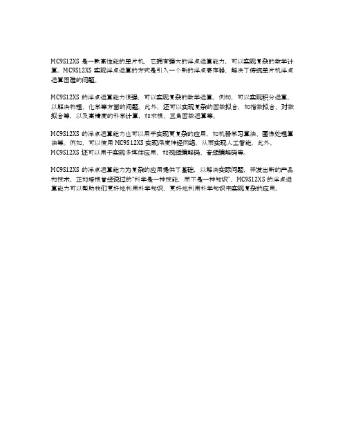
MC9S12XS是一款高性能的单片机,它拥有强大的浮点运算能力,可以实现复杂的数学计算。
MC9S12XS实现浮点运算的方式是引入一个新的浮点寄存器,解决了传统单片机浮点运算困难的问题。
MC9S12XS的浮点运算能力很强,可以实现复杂的数学运算。
例如,可以实现积分运算,以解决物理、化学等方面的问题。
此外,还可以实现复杂的函数拟合,如指数拟合、对数拟合等,以及高精度的科学计算,如求根、三角函数运算等。
MC9S12XS的浮点运算能力也可以用于实现更复杂的应用,如机器学习算法、图像处理算法等。
例如,可以使用MC9S12XS实现深度神经网络,从而实现人工智能。
此外,
MC9S12XS还可以用于实现多媒体应用,如视频编解码、音频编解码等。
MC9S12XS的浮点运算能力为复杂的应用提供了基础,以解决实际问题,开发出新的产品和技术。
正如培根曾经说过的“科学是一种技能,而不是一种知识”,MC9S12XS的浮点运算能力可以帮助我们更好地利用科学知识,更好地利用科学知识来实现复杂的应用。
飞思卡尔MC9S12XS128技术手册翻译AD
飞思卡尔MC9S12XS128技术手册(AD转换部分)英文资料:飞思卡尔MC9S12XS256RMV1官方技术手册1.1 XS12系列单片机的特点XS12系列单片机特点如下:·16位S12CPU—向上支持S12模糊指令集并去除了其中的MEM, WAV, WAVR, REV, REVW 五条指令;—模块映射地址机制(MMC);—背景调试模块(BDM);·CRG时钟和复位发生器—COP看门狗;—实时中断;·标准定时器模块—8个16位输入捕捉或输出比较通道;;—16位计数器,8位精密与分频功能;—1个16位脉冲累加器;·周期中断定时器PIT—4具有独立溢出定时的定时器;—溢出定时可选范围在1到2^24总线时钟;—溢出中断和外部触发器;·多达8个的8位或4个16位PWM通道—每个通道的周期和占空比有程序决定;—输出方式可以选择左对齐或中心对其;—可编程时钟选择逻辑,且可选频率范围很宽;·SPI通信模块—可选择8位或16位数据宽度;—全双工或半双工通信方式;—收发双向缓冲;—主机或从机模式;—可选择最高有效为先输出或者最低有效位先输出;·两个SCI串行通信接口—全双工或半双工模式·输入输出端口—多达91个通用I/O引脚,根据封装方式,有些引脚未被引出;—两个单输入引脚;·封装形式—112引脚薄型四边引线扁平封装(LQFP);—80引脚扁平封装(QFP);—64引脚LQFP封装;·工作条件—全功率模式下单电源供电范围3.15V到5V;—CPU总线频率最大为40MHz—工作温度范围–40 C到125 C第十章模拟—数字转换10.1 介绍ADC12B16C是一个16通道,12位,复用方式输入逐次逼近模拟—数字转换器。
ATD的精度由电器规格决定。
10.1.1 特点·可设置8位、10位、12位精度·在停止模式下,ATD转换使用内部时钟·转换序列结束后自动进入低耗电模式·可编程采样时间·转化结果可选择左对齐或右对齐·外部触发控制·转换序列结束后产生中断·模拟输入的16个通道为复用方式·可以选择VRH、VRL、 (VRL+VRH)/2特殊转换方式·转换序列长度1到16·可选择连续转换方式·多通道扫描·任何AD通道均可配置外部触发功能,并且可选择4种额外的触发输入。
飞思卡尔MC9S12XET256 SCI串口寄存器说明
串口寄存器说明该模块指南提供了串行通信接口(SCI)模块概述。
SCI的允许与外围设备和其他CPU异步串行通信。
1.1 SCI包括这些特征:•全双工或单线运行•标准标记/空间不归零(NRZ)格式•可选的IrDA1.4返回到零倒置(RZI)与可编程脉冲宽度格式•13位的波特率选择•可编程8位或9位数据格式•分别使能发射机和接收机•可编程极性对发射机和接收机•可编程发送器输出校验•两个接收器唤醒的方法:-唤醒空闲线- 地址标志唤醒•中断驱动的操作有八个标志:-发送器空- 传输完成- 接收器满- 空闲接收器输入- 接收器溢出-噪声误差-帧错误- 奇偶错误- 接收有效边缘唤醒- 发送冲突检测支持LIN-间隔检测支持LIN•接收帧错误检测•硬件奇偶校验•1 / 16位时间噪声检测1.2 操作模式SCI的功能相同在正常、特殊和仿真模式。
它有两种低功耗模式,等待和停止模式。
•运行模式•等待模式•停止模式1.3 寄存器说明1、波特率控制寄存器(SCIBDH、SCIBDL)SCIBDH和SCIBDL一起构成了一个16位的波特率控制寄存器。
SBR12~~SBR0为波特率常数。
IREN:红外调制模式使能位1 使能0 禁止TNP[0..1]:窄脉冲发射位,这些位使能SCI是否能发送一个1 / 16,3 /16,1/ 32或1 / 4的窄脉冲。
见表20-3。
SBR[0..12]:波特率设置位When IREN = 0 then,SCI baud rate = SCI bus clock / (16 x SBR[12:0])When IREN = 1 then,SCI baud rate = SCI bus clock / (32 x SBR[12:1])【说明】波特率发生器在复位后是禁止的,在设置TE、RE(在SCICR2寄存器中)后才会工作。
当(SBR[12:0] = 0 and IREN = 0) 或者(SBR[12:1] = 0 andIREN = 1),波特率发生器不工作。
MC9S12XS(DG)单片机--110108

CodeWarrior开发平台上可用汇编,也可用C语言编程。
CodeWarrior的使用
六、9S12XS/DG 的开发样例
1. 9S12XS/DG 的工程组织与通用I/O口的控制 2. PWM 输出编程 3.模拟信号采集 4定时器的功能与使用 5. 9S12XS/DG 的存储器控制 6. SCI/SPI串行数据通信 8.
;定义五个字的存储区,首址为X2
若要对X2的第三字赋值,可用如下语句:
STX X2+2
②数字常数/字符串常数定义伪指令:
格式: [<label>:] DC [.<size>] <expression> [ ,<expression>]…
功能:在Flash区定义一个size×n 个字节的存储区。
例: C1: DC .B $25
Freescale
车模用单片机原理与使用
讲座
车模电路组成
显示电路
路径检测 速度检测 电源电路
MCU
数据输入 电路
舵机控制
电机 速度控制
内容
一、飞思卡尔车模用单片机性能 二、9S12XS/DG 的硬件资源 三、9S12XS/DG 的硬件系统 四、9S12XS/DG的指令系统 五、 9S12XS/DG 的开发平台 六、9S12XS/DG 的开发样例
;定义一字节常数,即C1= $25
C2: DC .W $2538 ;定义一字常数,即C2= $2538
③常数赋值伪指令: 格式: <label>: EQU <expression> <label>: SET <expression> 功能:定义<label> 等于的值<expression>的值。 注意: <expression> 要有确定的值。 例: PI: EQU 3
飞思卡尔单片机 MC9S12 单片机应用系统开发平台下实时操作
计算机方向嵌入式计算机应用正在计算机领域迅速崛起,虽然该技术还不很成熟,但是它 的应用已经深入到社会各个领域,像办公自动化、民用消费品、计算机外设、机器人和武 器系统等等。
嵌入式系统,属于电子系统,包括微处理器或微控制器,嵌入式系统不是一般的计算 机,是隐藏或嵌入在各种系统中的计算机。主要用于控制领域,兼顾数据处理。而微控制 器即 MCU,MCU 的基本含义,在一片芯片上集成了中央处理单元(cpu)、存储器(RAM/ROM 等)、 定时器/计数器及多种输入\输出(I/O)接口的比较完整的数字处理系统。
MC9S12单片机原理及嵌入式应用开发技术第2章 单片机内部结构
4个要素 Two input data -- operands(操作数) instruction -- operation(运算) Status -- flag(标志位) one output data -- result(运算结果)
Quiz: 下面几个操作中,4要素分别为? A+B=C A>B? A >>= 1
ms CAN 1
ms CAN 0 or BDLC
PIM
AD0
AD1
PWM 8 CHAN
College of Communication Engineering, Jilin University
4
2.1 MC9S12XS单片机的性能
2.1.2 S12XS系列单片机主要功能模块
1.16位CPU 2.内部RAM或ROM: 3.A/D模块:16路8位、10位或12位; 4.CAN模块:支持CAN2.0A、B两种协议,1Mbps; 5.TIM模块:标准定时器,输入捕捉、输出比较 6.PIT模块:4通道24位递减计数器 7.PWM模块:8通道8位,或4通道16位,占空比可编程; 8.串口模块:两个SCI,支持LIN协议;一个SPI; 9.中断模块:最多20个带位中断的外部中断引脚,中断源 细分 为7级; 10.时钟模块:可通过内部锁相环使片内总线速度提升到最高 40MHz。
Memory peripheral
College of Communication Engineering, Jilin University
11
A complete CPU
College of Communication Engineering, Jilin University
12
CPU – the core of microcontroller
mc9s12xs128内存详解
Freescale Semiconductor Application Note Document Number: AN3497Rev. 0, 07/2007 Contents1IntroductionThe S12XS family is a next generation, cost competitive MCU solution targeting existing S12 customers and emerging markets. The S12XS family features a power- and code-efficient 16-bit core, on-board data flash(D-flash), an on-board frequency-modulated PLL, and offers flexibility and compatibility with the fully featured S12XE family.Target applications include smart junction boxes, seat controllers, HV AC, low-end engine control, body ECU, RKE receiver, door modules, and steering modules. The S12XS is pin compatible and emulatable with the XE family. Key features of the XE-family that are not included on XS family are: XGATE coprocessor, memory protection unit, and advanced emulated EEPROM functionality. The S12XE and S12XS families give customers flexibility from 64K up to 1M flash and packages from 64LQFP to 208MapBGA.1Introduction . . . . . . . . . . . . . . . . . . . . . . . . . . . . . . . . . . . 1 2Overview of S12XS Family . . . . . . . . . . . . . . . . . . . . . . . 2 3Memory . . . . . . . . . . . . . . . . . . . . . . . . . . . . . . . . . . . . . . 33.1P-Flash (Program Flash). . . . . . . . . . . . . . . . . . . . . 33.2D-Flash (Data Flash). . . . . . . . . . . . . . . . . . . . . . . . 43.3RAM . . . . . . . . . . . . . . . . . . . . . . . . . . . . . . . . . . . . 5 4Peripherals . . . . . . . . . . . . . . . . . . . . . . . . . . . . . . . . . . . 5 5Port Integration Module (PIM). . . . . . . . . . . . . . . . . . . . . 6 6Part IDs . . . . . . . . . . . . . . . . . . . . . . . . . . . . . . . . . . . . . . 6 7Summary. . . . . . . . . . . . . . . . . . . . . . . . . . . . . . . . . . . . . 7S12XS Family Compatibility Considerationsby:Lela GarofaloTSPGOverview of S12XS FamilyFor additional information on compatibility between S12XE and S12XS families, please refer to the Freescale application note, “Using the S12XE Family as a Development Platform for the S12XS Family,” (document AN3327).This document describes the differences and key similarities between the S12XS family members that must be considered when moving from a larger umbrella device with more memory and a larger package, to a smaller device with less memory and a smaller package.The topics discussed are:•Memory mapping and paging•Peripherals•Port integration module•Part IDs2Overview of S12XS FamilyThis document is meant to be used in conjunction with the S12XS family data sheet located at. Table1 gives an overview of the parts, available peripherals, and package options for each of the family members.Table1. Family FeaturesDevice Package XGATE CAN SPI SCI TIM PIT A/D PWM I/0S12XS256112 LQFPNotAvailable 1128ch4ch1/168ch9180 QFP1128ch4ch1/88ch59 64 LQFP1128ch4ch1/88ch44S12XS128112 LQFP1128ch4ch1/168ch91 80 QFP1128ch4ch1/88ch59 64 LQFP1128ch4ch1/88ch44S12XS64112 LQFP1128ch4ch1/168ch91 80 QFP1128ch4ch1/88ch59 64 LQFP1128ch4ch1/88ch44Memory3MemoryTable 2 gives an overview of the memory sizes available for the S12XS family. Local and global memory maps are compatible across the family. Out of reset, the family has equivalent maps and default values in the memory map control (MMC) registers. For devices with smaller amounts of memory, those areas unimplemented in the map will cause a reset if accessed.3.1P-Flash (Program Flash)The P-flash memory constitutes the main nonvolatile memory for applications. The P-Flash memory iscompatible for all flash devices in the S12XS family for all memory sizes in terms of functionality for program, erase, security, and protection setup. All family members have a single physical flash block that is equivalent to the defined flash size. Table 3 shows the physical flash block sizes in correlation to the global address.Table 2. Memory Sizes by DeviceDevice Flash R OM RAMData Flash9S12XS256256K — 12K 8K 9S12XS128128K — 8K 8K 9S12XS6464K —4K 4K 3S12XS256 —256K 12K — 3S12XS128—128K 8K — 3S12XS64—64K4K—Table 3. Physical P-Flash BlocksGlobal Address S12XS256S12XS128S12XS640x7C_0000256KB Flash BlockUnimplemented Unimplemented0x7D_FFFF 0x7E_0000128KB Flash BlockReserved0x7E_FFFF 0x7F_000064KB Flash Block 1The 9S12XS64 uses the 9S12XS128 die tested only for 9S12XS64 functionality. Accessing flash between address0x7E_0000 through 0x7E_FFFF does not cause an access error reset of device on a S12XS64 device with part ID $C1C0. The PartID register should be verified for the actual device.0x7F_FFFFMemoryFor all flash devices, programming and erase operations will be equivalent. Programming is done in phrases, or four word increments. Erase operations can be done in sectors or blocks. Simultaneous read while write and read while erase from P-flash is not available because there is only one physical block implemented on the 9S12XS family devices.Protection is compatible for all memory sizes of the S12XS family where implemented areas are equivalent.Security is equivalent for all S12XS family devices. The options/security byte is located at global address 0x7F_FF0F.PPAGEs for local memory maps are compatible across all family members where implemented areas are equivalent. Global memory map maps from higher order address down to a lower order address. Accessing unimplemented P-Flash space will cause an access error. An access error will cause the part to reset.3.2D-Flash (Data Flash)D-Flash will be compatible for all 9S12XS family flash devices where implemented areas are equivalent. 9S12XS256 and 9S12XS128 have an equivalent implemented amount of 8K. ROM devices do notimplement data flash. The global memory map maps from a lower order address to a higher order address.The D-flash can be accessed on the local memory map through the 1K DFLASH window through control of the EPAGE register. The EPAGE register has a default value of 0xFE out of reset. EPAGE 0xFE is unimplemented space on the S12XS family. Therefore, when accessing the D-Flash through the 1KD-Flash window, the EPAGE register must be written to with a valid EPAGE. Accessing unimplemented D-Flash space causes an access error. An access error causes the part to reset. Table 4 shows the valid EPAGEs and corresponding global addresses.Table 4. Data FlashEPAGE Global address 9S12XS2569S12X1289S12XS640x000x10_0000 8KB4KB0x10_3FFF 0x010x10_04000x10_7FF 0x020x10_08000x10_0BFF 0x030x10_0C000x10_0FFF 0x040x10_10000x10_13FF 0x050x10_14000x10_17FF 0x060x10_18000X10_1BFF 0x070x10_1C000x10_1FFFPeripherals3.3RAMRAM is compatible for all S12XS family devices where implemented areas are equivalent. Memory maps map from a higher-order address to lower-order address.The RPAGE register allows the user to page 4KB blocks into the RAM page window on the local memory map from address 0x1000 to 0x1FFF. The RPAGE default register value is 0xFD out of reset for all S12XS devices. Also, for all S12XS devices, addresses 0x2000 to 0x3FFF on the local memory map are fixed RAM pages for RPAGEs 0xFE and 0xFF. For the S12XS256, the default value of 0xFD allows for a linear address map to be accessible on the local map between addresses 0x1000 to 0x3FFF. For the S12XS128 and S12XS64 devices, RPAGE 0xFD is unimplemented space, and fixed page 0xFE (0x2000–3FFF) on the S12XS64 is unimplemented space. Accessing unimplemented space will cause an access error and the device to reset. For the S12XS128 and S12XS64, RPAGEs can be accessed through either the fixed RAM space or a valid RPAGE. Table 5 shows the location of RAM out of reset for the XS family.4PeripheralsAll peripherals are functionally compatible across the S12XS family. To maintain compatibility when developing on a larger memory and/or package option to move to a smaller device, pay careful attention to the pin-out and port routing options. A conclusive summary of the pin-outs for all three package options is available in the S12XS family can be found in the product preview, MC9S12XS256PB located at . Refer to table 6 for a complete summary of port routing options.The timer (TIM) module has eight channels available for all three package options. Channels IOC0, IOC1, and ICO2 have port-routing options (see Table 6). For the 80 QFP and 64 LQFP, if all eight PWM channels are used, then TIM channels IOC5 and IOC7 are not available simultaneously.The 112 LQFP has 16 ATD channels available, and all other package options have eight channels. To maintain compatibility when moving to smaller package options, use ATD channels 0–7 only.The pulse-width modulator (PWM) has eight channels available for all three package options. Channels PWM 4–7 have port routing options (see Table 6). PWM4 and PWM6 channels are available only on the 80 QFP and 64 LQFP if the port routing option is used to route to PT4 and PT6. Therefore, if all eight PWM channels are used, then TIM channels IOC5 and IOC7 are not available simultaneously for the 80 QFP and 64 LQFP.Table 5. RAM Global and Local AddressesGlobal Address Local Address RPAGE S12XS256S12XS128S12XS640x0F_D0000x10000xFD 12Kunimplementedunimplemented0x0F_DFFF 0x1FFF 0x0F_E0000x20000xFE 11Accessible through RP AGE window (0x1000 to 0x1FFF) by writing a valid RP AGE value to the RP AGE register.8K0x0F_EFFF 0x2FFF 0x0F_F0000x30000xFF14K0x0F_FFFF0x3FFFPort Integration Module (PIM)The S12XS family has two Serial Communication Interface (SCI) modules, SCI0 and SCI1 for all three package options. SCI1 has additional port routing options available. Refer to table 6 for port routing options.The Serial Peripheral Interface (SPI) has an additional port routing option (see Table 6).5Port Integration Module (PIM)The pin functions and priorities for all S12XS devices are the same after reset or a power-on reset (POR). Port routing options for PWM channels 4–7 and TIM channels 2–0 are controlled by the Port T Routing register (PTTRR). Likewise, port routing options for SCI1 and SPI0 are controlled by the Module Routingregister (MODRR). Table 6 shows the port routing options.6Part IDsFor the 9S12XS family, the part ID is located in two 8-bit registers: PARTIDH and PARTIDL (addresses 0x001A and 0x001B). The read-only value is a unique part ID for each device revision. Table 7 shows the assigned part ID number and mask-set number for each device.Table 6. Peripheral Port Routing Options 11x denotes reset condition, o denotespossible rerouting under software control.S C I 1S P I 0P W MT I M PM[1:0]o PM[5:2] o PP[2,0]o PP[2:0] o PP[7:4] x PS[3:2]x PS[7:4] x PT[2,0] x PT[7:4]oTable 7. Part IDsDevice Mask Set NumberPart ID MC9S12XS2560M05M $C0C0MC9S12XS1280M04M $C1C0MC9S12XS640M04M 1The 9S12XS64 uses the 9S12XS128 die tested for 9S12XS64 functionality only. An actual 9S12XS64 device may be done at a later time. A productchange notification will be posted in such an event. The PartlD register should be verified for actual device.$C1C0TBD$C2C0Summary 7SummaryThe key differences between the devices in the S12XS family are memory mapping. Although many of the peripherals are compatible, you should focus on the default pin/port-routing aspects of the specific peripherals to enable maximum scalability with anticipated future system needs. Part IDs are specific to each device. The S12XS64 device is a special case; any errata differences should be verified and associated to the corresponding part ID.This document is meant to be used with:•MC9S12XS Family Reference Manual•MC9S12XS Family Product Brief (document MC9S12XS256PB)•S12XCPUV2 Reference Manual (document S12XCPUV2)Document Number: AN3497Rev. 007/2007How to Reach Us:Home Page:Web Support:/support USA/Europe or Locations Not Listed:Freescale Semiconductor, Inc.Technical Information Center, EL5162100 East Elliot Road Tempe, Arizona 85284+1-800-521-6274 or +/supportEurope, Middle East, and Africa:Freescale Halbleiter Deutschland GmbH T echnical Information Center Schatzbogen 781829 Muenchen, Germany +44 1296 380 456 (English)+46 8 52200080 (English)+49 89 92103 559 (German)+33 1 69 35 48 48 (French)/supportJapan:Freescale Semiconductor Japan Ltd.Headquarters ARCO T ower 15F1-8-1, Shimo-Meguro, Meguro-ku,T okyo 153-0064Japan0120 191014 or +81 3 5437 9125support.japan@Asia/Pacific:Freescale Semiconductor Hong Kong Ltd.T echnical Information Center 2 Dai King StreetT ai Po Industrial Estate T ai Po, N.T., Hong Kong +800 2666 8080@For Literature Requests Only:Freescale Semiconductor Literature Distribution Center P .O. Box 5405Denver, Colorado 802171-800-441-2447 or 303-675-2140Fax: 303-675-2150LDCForFreescaleSemiconductor@Information in this document is provided solely to enable system and software implementers to use Freescale Semiconductor products. There are no express or implied copyright licenses granted hereunder to design or fabricate any integrated circuits or integrated circuits based on the information in this document.Freescale Semiconductor reserves the right to make changes without further notice to any products herein. Freescale Semiconductor makes no warranty, representation or guarantee regarding the suitability of its products for any particular purpose, nor does Freescale Semiconductor assume any liability arising out of the application or use of any product or circuit, and specifically disclaims any and all liability, including without limitation consequential or incidental damages. “Typical” parameters that may beprovided in Freescale Semiconductor data sheets and/or specifications can and do vary in different applications and actual performance may vary over time. All operating parameters, including “Typicals”, must be validated for each customer application by customer’s technical experts. Freescale Semiconductor does not convey any license under its patent rights nor the rights of others. Freescale Semiconductor products are not designed, intended, or authorized for use as components in systems intended for surgical implant into the body, or other applications intended to support or sustain life, or for any other application in which the failure of the Freescale Semiconductor product could create a situation where personal injury or death may occur. Should Buyer purchase or use Freescale Semiconductor products for any such unintended orunauthorized application, Buyer shall indemnify and hold Freescale Semiconductor and its officers, employees, subsidiaries, affiliates, and distributors harmless against all claims, costs, damages, and expenses, and reasonable attorney fees arising out of, directly or indirectly, any claim of personal injury or death associated with such unintended or unauthorized use, even if such claim alleges that FreescaleSemiconductor was negligent regarding the design or manufacture of the part. RoHS-compliant and/or Pb-free versions of Freescale products have the functionality and electrical characteristics as their non-RoHS-compliant and/or non-Pb-freecounterparts. For further information, see or contact your Freescale sales representative.For information on Freescale’s Environmental Products program, go to /epp .Freescale™ and the Freescale logo are trademarks of Freescale Semiconductor, Inc. All other product or service names are the property of their respective owners.© Freescale Semiconductor, Inc. 2007. All rights reserved.。
MC9S12系列及MC9S12X系列单片机解密
MC9S12系列及MC9S12X系列单片机解密致芯科技解密中心面向国内外客户提供MC9RS08系列单片机解密、MC9S12及MC9S12X系列单片机解密、MC68HC12系列单片机解密,对飞思卡尔芯片程序提取服务,我们依靠坚硬的技术为后盾,以最低的价格竭诚为您服务,以下是我们目前已经成功完成的单片机解密部分型号列表,更多可解密单片机型号不断更新中,如果您有MC9S12 系列芯片解密需求,欢迎来电来访咨询。
MC9S12系列芯片解密:MC9S12A系列单片机解密:MC9S12A32, MC9S12A64, MC9S12A128, MC9S12A256, MC9S12A512;MC9S12B系列单片机解密:MC9S12B32, MC9S12B64, MC9S12B96, MC9S12B128, MC9S12B256;MC9S12C系列单片机解密:MC9S12C32, MC9S12C64, MC9S12C96, MC9S12C128;MC9S12D系列单片机解密:MC9S12D32, MC9S12D64, MC9S12D96, MC9S12DB64, MC9S12DB128, MC9S12DG128, MC9S12DG256, MC9S12DJ64, MC9S12DJ128, MC9S12DJ256,MC9S12DP512, MC9S12DT128, MC9S12DT256, MC9S12DT512, MC9S12DE32, MC9S12DE64, MC9S12DE128;MC9S12E系列单片机解密:MC9S12GC系列单片机解密:MC9S12GC16, MC9S12GC32, MC9S12GC64, MC9S12GC96, MC9S12GC128;MC9S12H系列单片机解密:MC9S12H128, MC9S12H256;MC9S12HZ系列单片机解密:MC9S12HZ256, MC9S12HZ128, MC9S12HZ64;MC9S12K系列单片机解密:MC9S12KC128, MC9S12KG128, MC9S12KG256, MC9S12KT256, MC9S12KT256;MC9S12XB系列单片机解密:MC9S12XB128;MC9S12XD系列单片机解密:MC9S12XD64, MC9S12XD128, MC9S12XD256, MC9S12XD256, MC9S12XD384;MC9S12XE系列单片机解密:MC9S12XEG128, MC9S12XEP100, MC9S12XEP768, MC9S12XEQ384, MC9S12XEQ512, MC9S12XET256, MC9S12XDG128, MC9S12XDG256, MC9S12XDP512, MC9S12XDT256, MC9S12XDT512;MC9S12XF系列单片机解密:MC9S12XF512;MC9S12XHZ系列单片机解密:MC9S12XHZ256, MC9S12XHZ512;MC9S12XS系列单片机解密:MC9S12XS64, MC9S12XS128, MC9S12XS25;MC9S12NE系列单片机解密:MC9S12NE64;MC9S12P系列单片机解密:MC9S12P32, MC9S12P64, MC9S12P96, MC9S12P128;MC9S12Q系列单片机解密:MC9S12Q64, MC9S12Q96, MC9S12Q128;MC9S12UF系列单片机解密:MC9S12UF32;MC9S12XA系列单片机解密:MC9S12XA256, MC9S12XA512;。
- 1、下载文档前请自行甄别文档内容的完整性,平台不提供额外的编辑、内容补充、找答案等附加服务。
- 2、"仅部分预览"的文档,不可在线预览部分如存在完整性等问题,可反馈申请退款(可完整预览的文档不适用该条件!)。
- 3、如文档侵犯您的权益,请联系客服反馈,我们会尽快为您处理(人工客服工作时间:9:00-18:30)。
Freescale Semiconductor Product BriefMC9S12XS256PB Rev. 4, 11-Nov-2008MC9S12XS-FamilyLow Cost 16-Bit Microcontroller FamilyCovers MC9S12XS256, MC9S12XS128 and MC9S12XS64IntroductionThe new MC9S12XS-Family of 16-Bit micro controllers is a compatible, reduced version of theMC9S12XE-Family. These families provide an easy approach to develop common platforms from low-end to high-end applications, minimizing the redesign of software and hardware.Targeted at generic automotive applications and slave CAN nodes, some typical examples of these applications are:Body Controllers,Occupant Detection,Door Modules,RKE Receivers,Smart Actuators, Lighting Modules and Smart Junction Boxes amongst many others.For space-constrained applications, these products are also available in die format.The MC9S12XS-Family retains many of the features of the S12XE-Family including Error Correction Code (ECC) on Flash memory, a separate Data-Flash Module for code or data storage, a Frequency Modulated Locked Loop (IPLL) that improves the EMC performance and a fast ATD converter.MC9S12XS-Family will deliver 32-Bit performance with all the advantages and efficiencies of a 16-Bit MCU.It will retain the low cost,power consumption,EMC and code-size efficiency advantages currently enjoyed by users of Freescale’s existing16-Bit MC9S12and S12X MCU families.Like members of other S12X families,the MC9S12XS-Family will run16-Bit wide accesses without wait states for all peripherals and memories.FeaturesThe MC9S12XS-Family will be available in 112-Pin LQFP, 80-Pin QFP and 64-Pin LQFP package options and maintains a high level of pin compatibility with the S12XE-Family.In addition to the I/O ports available in each module,up to18further I/O ports are available with interrupt capability allowing Wake-Up from STOP or WAIT modes.The peripheral set includes MSCAN, SPI, two SCIs, 8-channel Timer, 8-channel PWM and up to 16-channel 12-bit ATD converter.Software controlled peripheral-to-port routing enables access to a flexible mix of the peripheral modules in the lower pin count package options.FeaturesFeatures of the MC9S12XS-Family are listed here.Please see Table1for memory options and Table2 for the peripheral features that are available on the different family members.16-Bit CPU12X •Upward compatible with MC9S12 instruction set•Enhanced indexed addressing•Access to large data segments independent of PPAGE•Note:five Fuzzy instructions are removed(MEM,WAV,WAVR,REV, REVW)Enhanced InterruptModule •Seven levels of nested interrupts•Flexible assignment of interrupt sources to each interrupt level.•External non-maskable high priority interrupt (XIRQ)•The following inputs can act as Wake-up Interrupts–IRQ and non-maskable XIRQ–CAN receive pins–SCI receive pins–Depending on the package option up to20pins on ports J,H and P configurable as rising or falling edge sensitiveSystem IntegritySupport •Power-on reset (POR)•Illegal address detection with reset•Low-voltage detection with interrupt or reset•Computer Operating Properly (COP) watchdog–Configurable as window COP for enhanced failure detection –Can be initialized out of reset using option bits located in Flash •Clock monitor supervising the correct function of the oscillatorFeaturesMemory Options •64K, 128K and 256K byte Flash•Flash General Features–64 data bits plus 8 syndrome ECC (Error Correction Code) bits allow single bit failure correction and double fault detection –Erase sector size 1024 bytes–Automated program and erase algorithm–Protection scheme to prevent accidental program or erase–Security option to prevent unauthorized access–Sense-amp margin level setting for reads•4K and 8K byte Data Flash space–16 data bits plus 6 syndrome ECC (Error Correction Code) bits allow single bit failure correction and double fault detection –Erase sector size 256 bytes–Automated program and erase algorithm•4K, 8K and 12K byte RAMOscillator (OSC_LCP)•Loop Control Pierce oscillator utilizing a 4MHz to 16MHz crystal –Current gain control on amplitude output–Signal with low harmonic distortion–Low power–Good noise immunity–Eliminates need for external current limiting resistor•Option for full-swing Pierce without internal feedback resistor utilizinga 2MHz to 40MHz crystal.•Transconductance sized for optimum start-up margin for typical crystalsInternally-Filtered Phase-Locked-Loop(IPLL)•Phase-locked-loop clock frequency multiplier–No external components required–Reference divider and multiplier allow large variety of clock rates –Automatic bandwidth control mode for low-jitter operation–Automatic frequency lock detector–Configurable option to spread spectrum for reduced EMC radiation (frequency modulation)Clock and Reset Generator (CRG)•COP watchdog•Real Time Interrupt•Clock Monitor•Fast wake up from STOP in self clock mode for power saving and immediate program execution•System reset generationFeaturesAnalog-to-Digital Converter (ATD)•16-channel, 12-bit Analog-to-Digital converter–8/10/12 Bit resolution–3µs, 10-bit single conversion time–Left or right justified result data–External and internal conversion trigger capability–Internal oscillator for conversion in Stop modes–Wake from low power modes on analogue comparison > or <= match–Continuous conversion mode–Multiplexer for 16 analog input channels–Multiple channel scans–Pins can also be used as digital I/OTimer (TIM)•8 x 16-bit channels for input capture or output compare •16-bit free-running counter with 8-bit precision prescaler • 1 x 16-bit pulse accumulatorPeriodic InterruptTimer (PIT)• 4 channel x 24-bit modulus down-count timers –Time-out interrupt–Time-out peripheral trigger•Start of timers can be alignedReal Time Interrupt(RTI)•Real Time Interrupt for task scheduling purposes or cyclic wake-up •Can be active in Pseudo Stop mode for low power precision timing tasksAsynchronous Periodic Interrupt(API)•Low Power wake-up timer–Internal oscillator driving a down counter–Trimmable to +/-10% accuracy across full operating range –Time-out periods range from 0.2ms to ~13s with a 0.2ms resolutionPulse Width Modulator (PWM)•Up to 8 channel x 8-bit or 4 channel x 16-bit Pulse Width Modulator –Programmable period and duty cycle per channel–Center- or left-aligned outputs–Programmable clock select logic with a wide range of frequenciesFeaturesMulti-ScalableController Area Networks(MSCAN)• 1 Mbit per second, CAN 2.0 A, B software compatible module –Standard and extended data frames–0 - 8 bytes data length–Programmable bit rate up to 1 Mbps•Five receive buffers with FIFO storage scheme•Three transmit buffers with internal prioritization•Flexible identifier acceptance filter programmable as:– 2 x 32-bit– 4 x 16-bit–8 x 8-bit•Wake-up with integrated low pass filter option•Loop back for self test•Listen-only mode to monitor CAN bus•Bus-off recovery by software intervention or automatically •16-bit time stamp of transmitted/received messagesSerial Peripheral Interface (SPI)•Configurable 8 or 16-bit data size •Full-duplex or single-wire bidirectional •Double-buffered transmit and receive •Master or Slave mode•MSB-first or LSB-first shifting•Serial clock phase and polarity optionsSerial CommunicationInterface (SCI)•Full-duplex or single wire operation•Standard mark/space non-return-to-zero (NRZ) format •Selectable IrDA 1.4 return-to-zero-inverted (RZI) format with programmable pulse widths•13-bit baud rate selection•Programmable character length•Programmable polarity for transmitter and receiver •Receive wakeup on active edge•Break detect and transmit collision detect supporting LINBackground Debug(BDM)•Background Debug Module (BDM) with single-wire interface –Non-intrusive memory access commands–Supports in-circuit programming of on-chip non-volatile memory –Supports securityFeaturesDebugger (xDBG)•Four comparators A, B, C and D to monitor CPU busses – A and C compares 23-bit address bus and 16-bit data bus with mask register– B and D compares 23-bit address bus only–Three modes: simple address/data match, inside address range or outside address range•64x64-bit circular trace buffer to capture change-of-flow addresses or address and data of every access•Tag-type or force-type hardware breakpoint requestsOn-Chip Voltage Regulator (VREG)•Two parallel, linear voltage regulators with bandgap reference •Low-voltage detect (LVD) with low-voltage interrupt (LVI)•Power-on reset (POR) circuit•Low-voltage reset (LVR)Input/Output •Up to 91 general-purpose input/output (I/O) pins depending on the package option and 2 input-only pins•Hysteresis and configurable pull up/pull down device on all input pins •Configurable drive strength on all output pinsPackage Options •112-pin low-profile quad flat-pack (LQFP), 20x20mm, 0.65mm pitch •80-pin quad flat-pack (QFP), 14x14mm, 0.65mm pitch•64-pin low-profile quad flat-pack (LQFP), 10x10mm, 0.5mm pitch •Known good die (KGD)Operating Conditions •Wide single Supply Voltage range3.135V to5.5V at full performance –Separate supply for internal voltage regulator and I/O allow optimized EMC filtering•40MHz maximum CPU bus frequency•Ambient temperature range –40°C to 125°C•Temperature Options:––40°C to 85°C––40°C to 105°C––40°C to 125°CBlock DiagramBlock DiagramFigure 1. MC9S12XS-Family Block Diagram4K … 12K bytes RAM RESET EXTAL XTAL4K … 8K bytes Data FlashBKGD VDDR Periodic Interrupt Clock Monitor Single-wire Background TESTVoltage RegulatorDebug Module VDD ATDMultilevel Interrupt ModuleP T A D SCI0SS SCKPS3PS0PS1PS2MOSI MISO SPI0P T S AN[15:0]PAD[15:0]VDDPLL8/10/12-bit 16-channel Analog-Digital Converter16-bit 8 channel TimerTIMAsynchronous Serial IF 8-bit 8 channelPulse Width ModulatorPWMPITPB[7:0]P T BPA[7:0]P T APK[7,5:0]P T K XIRQ IRQECLKPE4PE3PE2PE1PE0PE7PE6PE5P T EVDDF 64K … 256K bytes Flash CPU12XAmplitude Controlled Low Power Pierce or Full drive Pierce OscillatorCOP Watchdog PLL with Frequency Modulation optionDebug Module4 address breakpoints2 data breakpoints512 Byte Trace BufferReset Generation and Test Entry RXD TXD SCI1Asynchronous Serial IF RXD TXD PS7PS4PS5PS6PH3PH0PH1PH2P T H (W a k e -u p I n t )PH7PH4PH5PH6CAN0PM3PM0PM1PM2P T M msCAN 2.0BRXCAN TXCANPM7PM4PM5PM6Synchronous Serial IFAsync. Periodic Int.4ch 24-bit Timer P T J (W a k e -u p I n t )PJ7PJ6PT3PT0PT1PT2P T T PT7PT4PT5PT6PP3PP0PP1PP2P T P (W a k e -U p I n t )PP7PP4PP5PP6PWM3PWM0PWM1PWM2PWM7PWM4PWM5PWM6IOC3IOC0IOC1IOC2IOC7IOC4IOC5IOC6VDDA VSSA VRH VRLPJ1PJ0XCLKS/ECLKX2Block DiagramNOTEFor the 80QFP and 64LQFP package options,several peripheral functions can be routed under software control to different pins.Not all functions are available simultaneously. For details see Table 4.Table 1 Package and Memory Options of MC9S12XS-FamilyDevicePackage Flash RAMData Flash9S12XS256112 LQFP 256K 12K 8K80 QFP 64 LQFP KGD (Die)9S12XS128112 LQFP 128K 8K 8K80 QFP 64 LQFP KGD (Die)9S12XS64112 LQFP 64K 4K 4K80 QFP 64 LQFP KGD (Die)Table 2 Peripheral Options of MC9S12XS-Family MembersDevicePackageCANSCISPITIMPITA/DPWM9S12XS256112 LQFP 1218ch 4ch 16ch 8ch 80 QFP 1218ch 4ch 8ch 8ch 64 LQFP 1218ch 4ch 8ch 8ch KGD (Die)1218ch 4ch 16ch 8ch 9S12XS128112 LQFP 1218ch 4ch 16ch 8ch 80 QFP 1218ch 4ch 8ch 8ch 64 LQFP 1218ch 4ch 8ch 8ch KGD (Die)1218ch 4ch 16ch 8ch 9S12XS64112 LQFP 1218ch 4ch 16ch 8ch 80 QFP 1218ch 4ch 8ch 8ch 64 LQFP 1218ch 4ch 8ch 8ch KGD (Die)1218ch 4ch 16ch 8chPin Assignments Pin AssignmentsTable3 Port Availability by Package OptionPort112 LQFP80 QFP64 LQFP KGD (Die) Port AD/ADC Channels16/168/88/816/16Port A pins8848Port B pins8848 Port E pins inc. IRQ/XIRQ input only8848Port H8008Port J4204Port K7007Port M8668Port P8758Port S8448Port T8888Sum of Ports91594491 I/O Power Pairs VDDX/VSSX2/22/22/22/2Pin AssignmentsTable 4 Peripheral - Port Routing Options (1)NOTES:1.“X”denotes reset condition,“O”denotes a possible rerouting under software controlS C I 1S P I 0P W MT I M PM[1:0]OPM[5:2]OPP[2,0]OPP[2:0]OPP[7:4]XPS[3:2]XPS[7:4]XPT[2,0]XPT[7:4]O Table 5 Pin-Out Summary (1)LQFP 112QFP 80LQFP 64KGD (Die)Pin2nd Func.3rd Func.4th Func.5th Func.1111PP3KWP3PWM32222PP2KWP2PWM2IOC2TXD13333PP1KWP1PWM1IOC14444PP0KWP0PWM0IOC0RXD15--5PK36--6PK27--7PK18--8PK09559PT0IOC0106610PT1IOC1Pin Assignments117711PT2IOC2128812PT3IOC3139913VDDF 14101014VSS115111115PT4IOC4PWM416121216PT5IOC5PWM517131317PT6IOC6PWM618141418PT7IOC7PWM719--19PK520--20PK421--21PJ1KWJ122--22PJ0KWJ023151523BKGD MODC 24161624PB02517-25PB12618-26PB22719-27PB32820-28PB429211729PB530221830PB631231931PB732--32PH7KWH733--33PH6KWH634--34PH5KWH535--35PH4KWH436242036PE7XCLKS ECLKX23725-37PE6MODB 3826-38PE5MODA 39272139PE4ECLKTable 5 Pin-Out Summary (1)LQFP 112QFP 80LQFP 64KGD (Die)Pin2nd Func.3rd Func.4th Func.5th Func.Pin Assignments40282240VSSX241292341VDDX242302442RESET 43312543VDDR 44322644VSS345332745VSSPLL 46342846EXTAL 47352947XT AL 48363048VDDPLL 49--49PH3KWH350--50PH2KWH251--51PH1KWH152--52PH0KWH05337-53PE35438-54PE255393155PE1IRQ 56403256PE0XIRQ 57413357P A058423458P A159433559P A260443660P A36145-61P A46246-62P A56347-63P A66448-64P A765493765VDD 66503866VSS267513967P AD00AN0068--68P AD08AN08Table 5 Pin-Out Summary (1)LQFP 112QFP 80LQFP 64KGD (Die)Pin 2nd Func.3rd Func.4th Func.5th Func.Pin Assignments69524069P AD01AN0170--70P AD09AN0971534171P AD02AN0272--72P AD10AN1073544273P AD03AN0374--74P AD11AN1175554375P AD04AN0476--76P AD12AN1277564477P AD05AN0578--78P AD13AN1379574579P AD06AN0680--80P AD14AN1481584681P AD07AN0782--82P AD15AN1583594783VDDA 84604884VRH 85614985VRL (2)86624986VSSA 87--87PM788--88PM689635089PS0RXD090645190PS1TXD091655291PS2RXD192665392PS3TXD193--93PS4MISO094--94PS5MOSI095--95PS6SCK096--96PS7SS097675497TESTTable 5 Pin-Out Summary (1)LQFP 112QFP 80LQFP 64KGD (Die)Pin 2nd Func.3rd Func.4th Func.5th Func.Pin Assignments9868-98PJ7KWJ79969-99PJ6KWJ61007055100PM5SCK010********PM4MOSI010********PM3SS010********PM2MISO010********PM1TXCAN0TXD11057560105PM0RXCAN0RXD11067661106VSSX11077762107VDDX1108--108PK71097863109PP7KWP7PWM7110--110PP6KWP6PWM61117964111PP5KWP5PWM511280-112PP4KWP4PWM4NOTES:1. Table shows a superset of pin functions. Not all functions are available on all derivatives2. VRL and VSSA share single pin on 64-pin package optionTable 5 Pin-Out Summary (1)LQFP 112QFP 80LQFP 64KGD (Die)Pin2nd Func.3rd Func.4th Func.5th Func.Pin AssignmentsFigure 2.MC9S12XS-Family Pin Assignments 112-pin LQFP PackageVRH VDDAPAD15/AN15PAD07/AN07PAD14/AN14PAD06/AN06PAD13/AN13PAD05/AN05PAD12/AN12PAD04/AN04PAD11/AN11PAD03/AN03PAD10/AN10PAD02/AN02PAD09/AN09PAD01/AN01PAD08/AN08PAD00/AN00VSS2VDD PA7PA6PA5PA4PA3PA2PA1PA0P P 4/K W P 4/P W M 4P P 5/K P W 5/P W M 5P P 6/K W P 6/P W M 6P P 7/K W P 7/P W M 7P K 7V D D X 1V S S X 1P M 0/R X C A N 0/R X D 1P M 1/T X C A N 0/T X D 1P M 2/M I S O 0P M 3/S S 0P M 4/M O S I 0P M 5/S C K 0P J 6/K W J 6P J 7/K W J 7T E S T P S 7/S S 0P S 6/S C K 0P S 5/M O S I 0P S 4/M I S O 0P S 3/T X D 1P S 2/R X D 1P S 1/T X D 0P S 0/R X D 0P M 6P M 7V S S A V R LPWM3/KWP3/PP3TXD1/IOC2/PWM2/KWP2/PP2IOC1/PWM1/KWP1/PP1RXD1/IOC0/PWM0/KWP0/PP0PK3PK2PK1PK0IOC0/PT0IOC1/PT1IOC2/PT2IOC3/PT3VDDF VSS1PWM4/IOC4/PT4VREG_API/PWM5/IOC5/PT5PWM6/IOC6/PT6PWM7/IOC7/PT7PK5PK4KWJ1/PJ1KWJ0/PJ0MODC/BKGDPB0PB1PB2PB3PB4P B 5P B 6P B 7K W H 7/P H 7K W H 6/P H 6K W H 5/P H 5K W H 4/P H 4X C L K S /E C L K X 2/P E 7P E 6P E 5E C L K /P E 4V S S X 2V D D X 2R E S E T V D D R V S S 3V S S P L L E X T A L X T A L V D D P L L K W H 3/P H 3K W H 2/P H 2K W H 1/P H 1K W H 0/P H 0P E 3P E 2I R Q /P E 1X I R Q /P E 0Pins shown in BOLD are not available on the 80 QFPpackageMC9S12XS-Family112LQFP123456789101112131415161718192021222324252627281121111101091081071061051041031021011009998979695949392919089888786852930313233343536373839404142434445464748495051525354555684838281807978777675747372717069686766656463626160595857Pin AssignmentsFigure 3.MC9S12XS-Family Pin Assignments 80-pin QFP Package12345678910111213141516171819202122232425262728293031323334353637383940VRH VDDAP AD07/AN07P AD06/AN06P AD05/AN05P AD04/AN04P AD03/AN03P AD02/AN02P AD01/AN01P AD00/AN00VSS2VDD PA7PA6PA5PA4P A3P A2P A1P A0P B 5P B 6P B 7X C L K S /E C L K X 2/P E 7P E 6P E 5E C L K /P E 4V S S X 2V D D X 2R E S E T V D D R V S S 3V S S P L L E X T A L X T A L V D D P L L P E 3P E 2I R Q /P E 1X I R Q /P E 060595857565554535251504948474645444342418079787776757473727170696867666564636261MC9S12XS-Family80QFPPWM3/KWP3/PP3TXD1/IOC2/PWM2/KWP2/PP2IOC1/PWM1/KWP1/PP1RXD1/IOC0/PWM0/KWP0/PP0IOC0/PT0IOC1/PT1IOC2/PT2IOC3/PT3VDDF VSS1PWM4/IOC4/PT4VREG_API/PWM5/IOC5/PT5PWM6/IOC6/PT6PWM7/IOC7/PT7MODC/BKGDPB0PB1PB2PB3PB4P P 4/K W P 4/P W M 4P P 5/K P W 5/P W M 5P P 7/K P W 7/P W M 7V D D X 1V S S X 1P M 0/R X C A N 0/R X D 1P M 1/T X C A N 0/T X D 1P M 2/M I S O 0P M 3/S S 0P M 4/M O S I 0P M 5/S C K 0P J 6/K W J 6P J 7/K W J 7T E S T P S 3/T X D 1P S 2/R X D 1P S 1/T X D 0P S 0/R X D 0V S S A V R LPins shown in BOLD are not available on the 64QFP packagePin AssignmentsFigure 4.MC9S12XS-Family Pin Assignments 64-pin LQFP Package12345678910111213141516171819202122232425262728293031324847464544434241403938373635343364636261605958575655545352515049MC9S12XS-Family64LQFPVRH VDDAP AD07/AN07P AD06/AN06P AD05/AN05P AD04/AN04P AD03/AN03P AD02/AN02P AD01/AN01P AD00/AN00VSS2VDD P A3P A2P A1P A0P B 5P B 6P B 7X C L K S /E C L K X 2/P E 7E C L K /P E 4V S S X 2V D D X 2R E S E T V D D R V S S 3V S S P L L E X T A L X T A L V D D P L L I R Q /P E 1X I R Q /P E 0PWM3/KWP3/PP3TXD1/IOC2/PWM2/KWP2/PP2IOC1/PWM1/KWP1/PP1RXD1/IOC0/PWM0/KWP0/PP0IOC0/PT0IOC1/PT1IOC2/PT2IOC3/PT3VDDF VSS1PWM4/IOC4/PT4VREG_API/PWM5/IOC5/PT5PWM6/IOC6/PT6PWM7/IOC7/PT7MODC/BKGDPB0P P 5/K P W 5/P W M 5P P 7/K W P 7/P W M 7V D D X 1V S S X 1P M 0/R X C A N 0/R X D 1P M 1/T X C A N 0/T X D 1P M 2/M I S O 0P M 3/S S 0P M 4/M O S I 0P M 5/S C K 0T E S T P S 3/T X D 1P S 2/R X D 1P S 1/T X D 0P S 0/R X D 0V S S A /V R LMemory MapMemory MapFigure 5.MC9S12XS 16-bit Memory MapNORMAL SINGLE CHIPSPECIAL SINGLE CHIPVECTORS 16K Fixed Flash2K, 4K, 8K or 16K16K Page WindowPPAGE * 16K Flash Pages16K Fixed Flash (Remappable range)1K, 2K, 4K or 8K Protected Sector2K Register SpaceRAMUp to 8K Fixed RAM depending on derivativeBDM 0x00000xFFFF0xC0000x80000x40000x08000x10000xFF000x2000Protected Boot SectorRAMRPAGE * 4K pages accessible through 0x1000 - 0x1FFFReserved 0x0C00DFLASHEPAGE * 1K pages accessible through 0x0800 - 0x0BFFMemory MapFigure 6MC9S12XS Global Memory Map0x7F_FFFF0x00_00000x13_FFFF0x0F_FFFFDFLASHRAM0x00_07FFRP AGEPP AGE0x3F_FFFFCPU and BDMLocal Memory MapGlobal Memory MapFLASHF L A S H S I Z EUnimplementedFLASH0xFFFFVectors0xC0000x8000Unpaged 0x40000x10000x000016K FLASH window0x20000x08008K RAM4K RAM window2K REGISTERS 16K FLASHUnpaged 16K FLASH2K REGISTERSUnimplementedRAMUnimplementedSpaceRAM_LOWFLASH_LOWR A M S I Z E DF_HIGHDFLASH ResourcesReserved EPAGE1K DFLASH window0x0C00Revision HistoryRevision HistoryTable 6Memory Sizes per DerivativeDevice FLASH_LOW SIZE/PPAGE (1)NOTES:1. Number of 16K pages addressable via PPAGE register RAM_LOW SIZE/RPAGE (2)2. Number of 4K pages addressing the RAM.DF_HIGH EPAGE (3)3. Number of 1K pages addressing the DFLASH9S12XSx2560x7C_0000256K / 160x0F_D00012K / 30x10_1FFF 8K / 89S12XSx1280x7E_0000128K / 80x0F_E0008K / 20x10_1FFF 8K / 89S12XSx640x7F_000064K / 40x0F_F0004K / 10x10_0FFF4K / 4Table 7 Revision HistoryVersion Number Revision Date Author Description0.0012-Jan-2006DBInitial version. Based on 9S12XEFAMPP rev 0.100.0127-Mar-2006DBRemoved ECLKX2Added 48qfn mechanical diagramAltered 48pin and 52pin pinouts - share VRH/VDDA1 &VRL/VSSA1.Changed and simplified routing of peripherals.0.0229-Mar-2006DBFixed SPI signal ordering on Port M Fixed various typosAdded VRH, VRL, VDDA and VSSA to block diagram 0.034-Apr-2006RFRemoved SPI from PM[0:1,6:7]Added SCI1 to PM[0:1]Altered 48pin and 52pin pinouts0.046-Apr-2006RF Removed routing options for SCI1, PWM, TIM on 112 and 80Removed SPI from PP[0:3]0.057-Apr-2006RF Added SCI1 to PT[0,2]0.0628-Apr-2006DBUpdated Block Diagram to reflect peripheral routings.Added SPI0 routing to PS[7:4] in Table 4.Revision HistoryMC9S12XS-Family, Rev. 4Freescale Semiconductor 210.0722-Jun-2006DB Changed VSSR to VDD3.DFlash sector size 256 bytes.Added Global Memory map Figure 6 & Table 6.Removed 5 Fuzzy instructions.0.0816-Aug-2006DB Changed Interrupt Module to 7 levels of interrupt.0.0928-Nov-2006DB Removed 52QFP and 48LQFP package options Added 64LQFP package optionModified PortT pinout on 48QFN,108-Dec-2006DB Minor formatting changes21-Jun-2007DB Removed 48QFN package optionAdded 64qfp option for XS256Change routing option to remove PWM0-3 from PT0-3319-Jun-2007DB Correction to Table 2: 8PWM channels available in all packages.411-Nov-2008Removed ROM optionsAdded KGD optionsRemoved package drawings Table 7 Revision HistoryVersion Number Revision Date Author DescriptionMC9S12XS256PBRev. 4, 11-Nov-2008How to Reach Us:USA/Europe/Locations not listed:Freescale Semiconductor Literature Distribution P .O. Box 5405, Denver, Colorado 802171-800-521-6274 or 480-768-2130Japan:Freescale Semiconductor Japan Ltd.SPS, T echnical Information Center3-20-1, Minami-AzabuMinato-kuTokyo 106-8573, Japan81-3-3440-3569Asia/Pacific:Freescale Semiconductor H.K. Ltd.2 Dai King StreetTai Po Industrial EstateTai Po, N.T. Hong Kong852-********Learn More:For more information about Freescale Semiconductor products, please visitInformation in this document is provided solely to enable system and software implementers to use Freescale Semiconductor products. There are no express or implied copyright licenses granted hereunder to design or fabricate any integrated circuits or integrated circuits based on the information in this document.Freescale Semiconductor reserves the right to make changes without further notice to any products herein. Freescale Semiconductor makes no warranty, representation or guarantee regarding the suitability of its products for any particular purpose,nor does Freescale Semiconductor assume any liability arising out of the application or use of any product or circuit, and specifically disclaims any and all liability,including without limitation consequential or incidental damages.“Typical”parameters which may be provided in Freescale Semiconductor data sheets and/or specifications can and do vary in different applications and actual performance may vary over time.All operating parameters,including “Typicals”must be validated for each customer application by customer’s technical experts.Freescale Semiconductor does not convey any license under its patent rights nor the rights of others.Freescale Semiconductor products are not designed,intended,or authorized for use as components in systems intended for surgical implant into the body, or other applications intended to support or sustain life,or for any other application in which the failure of the Freescale Semiconductor product could create a situation where personal injury or death may occur. Should Buyer purchase or use Freescale Semiconductor products for any such unintended or unauthorized application,Buyer shall indemnify and hold Freescale Semiconductor and its officers,employees,subsidiaries,affiliates,and distributors harmless against all claims, costs, damages, and expenses, and reasonable attorney fees arising out of, directly or indirectly, any claim of personal injury or death associated with such unintended or unauthorized use, even if such claim alleges that Freescale Semiconductor was negligent regarding the design or manufacture of the part.Freescale™ and the Freescale logo are trademarks of Freescale Semiconductor, Inc. All other product or service names are the property of their respective owners.© Freescale Semiconductor, Inc. 2007.。