TDA集成块引脚功能
SC1088(TDA7088T)调频调频收音机资料
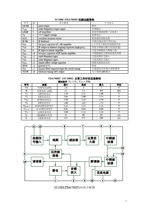
TDA7088T(SC1088)正常工作时的直流特性SC1088(TDA7088T)内部方框图SC1088(TDA7088T)典型接线图使用SC1088(TDA7088T)组装调频接收机●IC产品型号:SC1088(TDA7088T)●产品名称:自动调谐的调频收音机接收电路●产品概述:SC1088是一块适用于单声道便携式或手掌式超小型调频收音机的专用电路,它采用先进的双极型工艺制造,在外围元件的数量、尺寸及成本上变得很重要时,可优先选用该电路。
该电路中含有一个中频(IF)约为70kHz的锁相环回路(FLL),选择性通过一有源RC 滤波器来调整,与中频相应的未调谐信号和低输入信号由静噪电路抑制。
●主要特点:含有单声道收音机从天线接收到音频输出的所有功能静噪功能外接一只变容二极管可进行自动搜寻调谐采用内部AFC电路可进行机械调谐可支持调幅接收应用电源极性反接保护电源电压低至1.8V仍可正常工作●应用:机械调谐方式:可用、也可不用内置的AFC电路自动调谐方式:可实现单方向(向高频方向)的自动搜寻调谐功能;包括复位功能,即回到频段的最低段●封装SC1088——SOP-16-225-1.27●FM自动选台调谐收音机的制作(TDA7088与SC1088引脚及工作原理完全一样,可互换):【功能】本文介绍的袖珍FM电脑选台收音机采用飞利浦公司开发生产的TDA7088T(SC1088)集成块,采用16脚双列扁平封装,工作电压为3V,该电路除包含FM 收音机从天线接收到鉴频输出音频信号的全部功能外,还设有搜索调谐电路、信号检测电路、静噪电路以及压缩中频频偏的频率锁定环FLL电路。
TDA7088T(SC1088)电路的中频频率设计为70kHz,外围电路不用中频变压器,其中频选择由电路内部RC中频滤波器来完成。
该机像数字调谐收音机那样采用电调谐按钮(RUN),另一只是复位按钮(RESET)。
电路接通电源后,按一下搜索按钮,电路自动地由频率低端向高端搜索电台,一旦搜索到电台信号,调谐自动停止。
TDA2025-4558D应用-变压器资料

TEA2025是欧洲生产的双声道功率放大集成电路,该电路具有声道分离度高、电源接通时冲击噪声小、外接元件少,最大电压增益可由外接电阻调节等特点,应用于袖珍式或便携式立体声音响系统中作功率放大。
1.TEA2025内电路方框图及引脚功能TEA2025集成块内部主要由两路功能相同的音频预放、功放、去耦、驱动电路、供电电路等组成,其集成块的内电路方框图及双声道应用电路如图所示。
该IC采用16脚双列直插式封装,其集成电路的引脚功能及数据见表所列。
2.TEA2025主要电参数(1)极限使用条件。
电源电压Vcc=15V,输出峰值电流10=1.5A。
(2)主要电参数。
TEA2025集成电路工作电源电压范围为3--12 V.典型工作电压6-9 V。
在Vcc=9 V,RL=8。
Ta=25℃条件下,有以下主要电参数。
静态电流ICQ 最大值为50 mA,典型值为40 mA。
电压增益GV 双声道时的最大值为47 dB,最小值为43 dB,典型值为45 dB;BTL时的最大值为53 dB,最小值为49 dB,典型值为51 dB。
输出功率PO 当THD=10%,P=1 kHz时,双声道时的典型值为1.3 W,BTL时的典型值为4.7 W。
谐波失真THD 当F=1 kHz,Po=250 mW,RL=4。
时,双声道时的最大值为1.5%,典型值为0.3%; BTL时的典型值为0.5%.3.TEA2025典型应用电路TEA2025集成电路的输出功率由电源电压和负载阻抗大小决定。
既可以构成双声道功放,又可以组成BTL功放。
其集成块的双声道典型应用电路如图所示,其集成块的BTL典型应用电路如图所示。
4.电路工作过程以双声道电路为例,音频信号经电容祸合从TEA2025的⑦、⑩脚输入,先经预放大后加到功率放大器,放大后的音频信号从②、15脚输出,由输出祸合电容耦合去驱动喇叭发声。
TEA2025集成块的①脚专用于BTL方式时用,当采用双声道方式时,应将其悬空不接。
TDA8359J场输出功率芯片引脚功能参数及图纸资料教学文稿
T D A8359J场输出功率芯片引脚功能参数及图纸资料
TDA8359J场输出功率芯片引脚功能参数及图纸资料
来源:/访问次数:5049 发表时间06-19编辑:bjjdwx 作者:
TDA8359 -场输出功率放大芯片引脚功能参数及应用图纸资料
飞利浦半导体公司生产的场输出功率放大芯片该芯片需要很少的外部元件高效率充分直流耦合垂直桥输出线路垂直短的上升和下降反激开关时间·内置保护电路热保护电路·改善EMC性能,由于差分输入。
多用在各种品牌crt电视机场输出电路,应广大会员要求特整理该芯片的引脚功能和参数供大家维修参考。
概述:TDA8359J 是用于对应25 至200Hz 场频的90°及110°色彩偏转系统的功率电路,也可用于4:3 及16:9 的显像管。
此IC 有一个场偏转输出电路,可作为一个高效G 级系统运行。
在单一正电压供电的情况下,全桥输出电路允许偏转线圈直流耦合。
此IC 采用低电压DMOS(LVDMOS)处理过程来制造,其内部包含双极性、CMOS 及DMOS 器件。
由于没有二次击穿问题,输出级可使用DMOS 三极管。
6 VFB 回扫供电电压47.5v
7 OUTA 输出A 10.5v
8 GUARD 保护输出0.3v
9 FEEDB 反馈输入10.5v。
TDA8362集成块引脚功能

TDA8362集成块引脚功能1.锁相环输入引脚(VCO-IN):此引脚接收来自外部的矩形信号,用于电视恢复。
2.锁相环反相输入引脚(VCO-INB):此引脚接收来自外部的反相矩形信号,用于电视恢复。
3.滤波器引脚(VCO-OUT):此引脚通过外部电容和电阻连接到地,用于滤除高频噪声。
4.滤波器引脚(VCO-OUTB):此引脚通过外部电容和电阻连接到地,用于滤除高频噪声。
5.音频抗混叠引脚(AFC-IN):此引脚接收来自外部音频源的音频信号,用于抗混叠。
6.音频抗混叠输出引脚(AFC-OUT):此引脚通过外部电容和电阻连接到地,用于提供抗混叠功能。
7.音频中频引脚(IF-IN):此引脚接收来自外部中频信号源的信号,用于电视音频。
8.音频中频反相输入引脚(IF-INB):此引脚接收来自外部中频信号源的反相信号,用于电视音频。
9.音频中频输出引脚(IF-OUT):此引脚通过外部电容和电阻连接到地,用于输出中频信号。
10.音频中频反相输出引脚(IF-OUTB):此引脚通过外部电容和电阻连接到地,用于输出反相中频信号。
11.色彩CPU输入引脚(CPU-IN):此引脚接收来自外部的色彩信号,用于电视的色彩处理。
12.色彩CPU反相输入引脚(CPU-INB):此引脚接收来自外部的反相色彩信号,用于电视的色彩处理。
13.色彩CPU输出引脚(CPU-OUT):此引脚通过外部电容和电阻连接到地,用于输出处理后的色彩信号。
14.色彩CPU反相输出引脚(CPU-OUTB):此引脚通过外部电容和电阻连接到地,用于输出反相处理后的色彩信号。
15.场频偏移引脚(VCO-COR):此引脚接收来自外部场频信号源的反馈信号,用于控制水平线锁定。
16.场同步输入引脚(SYNC-IN):此引脚接收来自外部的场频信号源的输入信号。
17.场同步反相输入引脚(SYNC-INB):此引脚接收来自外部场频信号源的反相输入信号。
18.场同步输出引脚(SYNC-OUT):此引脚输出同步信号,用于同步其他设备。
tda8362集成块引脚功能(Tda8362integratedblockpinfunction)
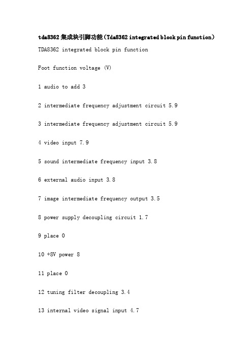
tda8362集成块引脚功能(Tda8362 integrated block pin function)TDA8362 integrated block pin functionFoot function voltage (V)1 audio to add 32 intermediate frequency adjustment circuit 5.93 intermediate frequency adjustment circuit 5.94 video input 7.95 sound intermediate frequency input 3.86 external audio input 3.87 image intermediate frequency output 3.58 power supply decoupling circuit 1.79 place 010 +8V power 811 place 012 tuning filter decoupling 3.413 internal video signal input 4.714 resolution control 0~4.315 external video signal input 4.216 chroma signal input AV/TV switch (TV/AV1/S/AV2) 0/7.6/4/7.617 brightness control 0~4.218 B output 2.719 G output 2.720 R output 2.721 RGB and blanking input 0.522 R input 3.423 G input 3.424 B input 3.425 contrast control 0~3.626 color saturation control 0~4.427 hue control input and SECAM.CVBS output 0~5/628 B-Y input 3.829 R-Y input 3.830 R-Y output 1.531 B-Y output 1.5324.43 baseband and SECAM identification output (P.N/S) 0.5/533 color synchronous phase detector 5.134 3.58MHZ crystal connected 1.435 4.43MHZ crystal connected 236 line starting oscillation power supply 8.4The 37 line drives output 0.538 lines reverse journey into "sand fort" pulse 2.839 line center adjustment and filter 2.840 row phase filter circuit 3.941 field reverse input 2.442 starts and 2.7 starts43 field drive output 144 AFC output 4.745 If input 4.146 If input 4.147 AGC tuner output 8.848 AGC detection 3.849 RF AGC regulation 1.350 audio output 3.351 audio demodulation, decoupling 4.152 brightness signal power decoupling 6.5TDA3862 is composed of 7 foot IC output video signal by IC, 7 feet of the triode emitter output by the transistor buffer by the emitter output by 4.5MHz, 5.5MHz, 6.0MHz, 6.5MHz signal notch respectively into the integrated circuit 4053 12 feet and 13 feet, with the inside of the conversion switch. The signal is switched through the 9 pin of the integrated circuit 4053 and the 10 pin control and the AV input terminal, and the final signal is output by the 15 pin of the integrated circuit 4053.The brightness and contrast signals of various standard signals are separated from each other within the integrated circuit. Of course, you must be sure of the color system of the current signal before you proceed with bright color separation,This is also done internally with IC. In brightness separation, the only pin associated with the external circuit is the 12 pin,which is used to adjust the frequency of the internal color and filter.1. black, but the character display normal: 1. Check whether the work in the AV state. The test of IC. 17 feet and 25 feet if the voltage is too low. 3. Test the character background blanking voltage (IC 21 feet) is too high, too high will make the whole picture is hidden, the foot on the ground to see if short circuited image is caused by. The sand will be abnormal. Black screen character, not what was 38 feet IC and short circuit on the screen, and if the 38 feet to get it open will appear black, normal to abnormal character.2. colorless or achromatic: a television set made up of TDA8362 and TDA4665. NTSC normal, but PAL colorless maintenance, you can get TDA4665 down. Connect IC's 30 foot and 29 foot, 31 feet and 28 feet each with a capacitor 0.1 F, connect to see if the TV has color appear, if there is, that is DTA4665 finished. (sometimes the color takes a moment to come.).The IC line oscillation is done inside the IC, but it requires the IC's 35 pin oscillator to provide the effect signal, so the circuit can work properly.When a signal is sent from the AV/TV or S terminal, a video signal or a luminance signal is separated from the internal synchronization of the IC to produce a composite sync pulse to further separate the trip / field synchronization signal. The 36 pin of the IC is to supply 8.2V power to the small signal processing circuit, which requires a higher power supply.The crystal oscillation circuit in the 35 foot line with the help of vibration, vibration signal and the synchronous signal phase in AFC1 circuit, dual filter time constant by 40 feet of RC components generates an error signal, the oscillation frequency control right. The oscillation signal is compared with the input pulse signal of the IC 38, and the central control of the line scanning is realized by setting the 39 pin external circuit of the IC to change the phase. Finally, after the pre excitation signal, the output signal from the IC pin 37 output IC pin 37 is open to the external power supply mode, or can not work can sometimes be rather baffling and strange phenomena such as: fault IC 49 feet appeared.There is no grating fault. TDA8362 36 foot power requirements higher, bad, there will be a series of strange phenomena.TDA8362's 47 foot problems can cause image shake and distortion. IC between 1 feet and 2 feet, and connect resistor 200K, can open the color channelCommon faults:I. accompanying soundMost of the faults that have no audio are in the audio intermediate frequency input circuit, audio output, audio frequency amplification circuit and de coupling sound demodulation.1. the most common non audio fault location is the IC audio intermediate input external capacitor deterioration leakage.In addition, the three groups of filters in the three audio signal circuits are damaged by any of the components of the filter, and the group has no sound.2., IC 1 feet audio output, audio to aggravate and IC 51 feet decoupling, audio demodulation circuit if the capacitor, short circuit or leakage, will lead to no sound.The 50 pin of the 3. IC is an audio output (controlled) circuit, and if an external capacitor is leaking, it will cause no sound.Two, grating, no imageOneThe most common causes is in IC 46, 46 feet is the intermediate frequency input circuit, such as frequency of the input circuit coupling capacitor deterioration or short circuit can lead to a grating without image, but the noise points weak, while the IC of 45, 46 feet if the input circuit of external resistance will lead to light, the gate open no image.2. IC 48 pin AGC detection circuit, external capacitor deterioration short-circuit will lead to grating without image, but there are weak noise points.The 3. IC 31 pin is a + (B-Y) output circuit, and the external resistance is open to a raster without an image.4. IC internal damage also occurs with grating without image.Four. The image is shaking and twistingThe most common is the 47 pin IC AGC tuner tuner output circuit to filter capacitor leakage or deterioration and AGC detection circuit, AGC adjusting element damage.Five, bad characters1.IC 24 pin blue character input external capacitor leakage.2. IC 22 pin red character input external capacitor leakage.IC's 52 foot special, its English name is "BAND GAP", meaning "band gap"". Its role is the reference voltage, and the role of the pin and its external components is to use band gap technology to achieve voltage regulation, so the IC 52 pin voltage is very stable 6.5V. This pin is mainly used in circuit such as field scanning, which requires high stability voltage. If the IC 52 pin circuit is abnormal, it will cause serious changes in amplitude and linearity of the field, even the fault of the horizontal bright line.IC can be used to adjust for 39 feet or center line, because the IC is not set for the line in the PAL/NTSC oscillator respectively by IC standard 34, 35 feet outside the crystal 2.58MHz, connected 4.43MHz frequency automatically generated. IC 39 feet for the second phase back end, change the external adjustable resistance can change the amount of delay (as well as the center of the image.). IC 40 feet for the first line of the phase back end, the loop of the image of the line synchronization pulse and pulse shock compared to control theoscillation frequency with the error voltage, and make the TV signals with the same frequency and phase.HeipingWhether the 48 foot test voltage IC is greater than 6V the foot when the foot video squelch function, when the voltage is greater than 6V, will put the output off screen caused no light. Is the 16 pin voltage of the IC 0V?. The foot selects the control pin for the video signal. If it is high, the IC is in the AV state, and the 21 pin voltage of the IC is 0V. When the foot is larger than 1V, the signal sent to the visual board is a character signal. When the voltage of the foot is 0V, the signal sent to the visual board is the video signal after the demodulation. IC 17, 25 feet brightness, contrast, control voltage is too low. Is the pulse of the 38 pin output of the IC normal?.The same types have TDA83618362 and OM8361 as well as OM8362.。
TDA8360A引脚功能Microsoft Word 文档
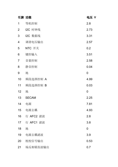
引脚功能电压V1 等机控制 2.82 I2C 时钟线 2.733 I2C 数据线 3.314 调谐电压输出 2.575 NTC 开关0.26 键控输入 3.517 音量控制 2.588 静音控制0.049 地010 频段选择控制A 4.9911 频段选择控制B 0.0312 地013 SECAM 2.2514 电源7.8115 电源去耦 4.9316 行AFC2 滤波 2.817 行AFC1 滤波 3.818 地019 电源去耦滤波 3.920 枕校信号输出0.5321 场反相锯齿波输出0.722 场正相锯齿波输出0.723 中放输入 1.824 中放输入 1.825 基准电流输入 3.826 场锯齿波形成电容 3.727 高放AGC 输出 1.928 去加重电容 3.329 音频解调滤波 2.230 地031 伴音窄带锁相环滤波/ 伴音中频输入 2.232 自动音量调整滤波0.233 行驱动输出0.534 沙堡脉冲输出0.4535 外部音频信号输入 3.636 高压反馈/ 过压保护输入 1.737 中放锁相环滤波 2.3438 视频信号输出 3.039 电源7.840 视频信号输入 3.841 地042 AV 视频/S 端子亮度信号输入 3.243 S 端子色度信号输入 1.4544 中放音频信号输出 3.345 第二RGB/YUV 插入控制 2.246 DVD/CB 信号输入 2.4747 DVD/Y 信号输入 2.4748 DVD/CR 信号输入 2.3149 ABL 束电流限制输入/ 场保护输入 6.0850 暗电流检测输入 3.2551 R 基色输出 3.8852 G 基色输出 2.7853 B 基色输出 3.4954 电源055 地056 电源 3.357 地 1.7358 晶振信号输入 1.7359 晶振信号输出 1.7960 复位061 电源 3.5162 AV 选择控制输出1 0.0763 AV 选择控制输出2 0.0664 遥控信号入 4.97 TDA9370与TDA9373它集TV信号处理、微处理控制于一体的超级大规模64脚芯片电路,它的详细内容介绍很多的技术资料都有介绍。
创维21D88AA(TDA12155PSN33AF8)的功能脚和电压脚资料【精选..
1 脚:视频输出(3P90、3P91 机芯无AV 输出功能)l 2 脚:接+5V,第二电源电压(IF 和伴音供电)l 3 脚:接+8V,音频输出、音效处理(TDA12155)供电l 4 脚:中频锁相环滤波器l 5 脚:接地2 (IF 和伴音部分)l 6 脚:伴音解调去耦电容l 7 脚:自动音量控制电容l 8 脚:EHT 反馈输入/过压保护输入l 9 脚:高放(调谐器)AGC 电压输出l 10 脚:基准电流输入l 11 脚:场锯齿波形成电容l 12 脚:图像中放输入2l 13 脚:图像中放输入1l 14 脚:场扫描激励信号A 输出l 15 脚:场扫描激励信号B 输出l 16 脚:东西校正激励电压输出(TDA12155)l 17 脚:能带去耦电容l 18 脚:SECAM 制色度PLL 去耦l 19 脚:接地1 (彩色处理、同步和几何部分)l 20 脚:第一鉴相器滤波器l 21 脚:第二鉴相器滤波器l 22 脚:接+5Va,第二电源电压,该机芯取自行扫描(彩色处理、同步和几何失真校正部分供电)l 23 脚:数字电路部分去耦l 24 脚:晶体振荡器输出l 25 脚:晶体振荡器输入l 26 脚:I/O 口,未用l 27 脚:静音控制输出(高电平静音,低电平解除)l 28 脚:按键信号输入KEY2l 29 脚:按键信号输入KEY1l 30 脚:I/O 口,未用l 31 脚:AV 伴音输入切换信号输出1l 32 脚:AV 伴音输入切换信号输出2l 33 脚:+3.3V(MCU I/O 部分供电)l 34 脚:IIC 总线数据信号线;l 35 脚:IIC 总线时钟信号线;l 36 脚:EEPROM 的保护(高电平保护)l 37 脚:为待机信号输出端(高电平待机)l 38 脚:掉电检测中断输入(低电平触发中断,关电源时可消音且消亮点)l 39 脚:红外遥控信号输入l 40 脚:+3.3V(MCU 核心部分供电)l 41 脚:接地5(MCU 数字部分供电)l 42 脚:烧OTP 时需接9V 供电l 43 脚:+3.3V(MCU 模拟及数字部分供电)l 44 脚:蓝基色输出l 45 脚:绿基色输出l 46 脚:红基色输出l 47 脚:白平衡检测消隐电流输入/场保护输入l 48 脚:ABL (平均束流限制器输入)l 49 脚:分量信号Cb 输入l 50 脚:分量信号Y 输入l 51 脚:分量信号Cr 输入l 52 脚:亮度信号输出l 53 脚:同步分离亮度信号输入l 54 脚:接+5V,第三电源电压(CVBS、滤波、YPBPR、RGB 等部分)l 55 脚:接地3 (CVBS、滤波、YPBPR、RGB 等部分)l 56 脚:行扫描驱动信号输出l 57 脚:行反峰输入/沙堡脉冲输出l 58 脚:右声道音频输出l 59 脚:左声道音频输出l 60 脚:音视频输入脚,未用l 61 脚:右声道音频输入l 62 脚:视频输入1l 63 脚:左声道音频输入l 64 脚:视频输入2调试说明 本调试手册适应模拟机芯3P90、4P90 以及模拟高清机芯3P91、4P91,涵盖21 寸、24寸、25 寸、29 寸系列普通管及短管,主芯片采用NXP 的新一代UOCTOP 系列芯片TDA11105(用于21 寸普通管)和TDA12155(有高、低音、响度控制以及EW 校正功能,用于短管和大尺寸普通管);模拟高清方案采用晶宝利公司的PLM1000 芯片。
TDA4856的引脚功能 和正常电压数据
27,频率/电压转换电压缓冲输出 1.7V
28,行振荡基准外接电流 2.5V
29,行振荡外接电热器 4.6V
30,PLL2外接滤波器/软启动 5V
31,高电压变动引起的行幅变化补偿输入 5.1V
32,水平与垂直动态聚焦输出 6.2V
18,I2C总线时钟输入 5.5V
19,总线数据输入/输出 4.9V
20,左右枕校不平衡校正控制信号输出 3.9V
21,高压变动引起的场幅变化补偿输入 5.0V
22,场幅控制外接电热器(场幅控制AGC)2.8V
23,场振荡外接电阻器 3.0V
24,场振荡外接热器 2.7V
25,地
9,X射线保护复位选择输入 11.7V
10,VCC 11.7V
11,左右枕校输出 2.4V
12,场输出2(上升场锯齿波) 0.9V
13,场输出1(下降场锯齿波)0.9V
14,场同步输入 0V
15,行同步/复合同步信号输入 5.0V
16,视频钳位脉冲/场消隐信号输出 0.8V
17,行同步失锁/保护/场消隐输出 0.2V
TDA4856的引脚功能 和正常电压数据
1,行逆程脉冲输入 0.3V
2,X射线保护输入 5.2V
3,B+控制OTA(运算跨导放大器)输出 5.2V
4,B+控制比较输入 4.0V
5,B+控制OTA输入 5.0V
6,B+控制驱动输出 2.9V
7,电源地
8,行激励输出 1.1V (注意:如果电压为10左右,集成块保护,行停振)
- 1、下载文档前请自行甄别文档内容的完整性,平台不提供额外的编辑、内容补充、找答案等附加服务。
- 2、"仅部分预览"的文档,不可在线预览部分如存在完整性等问题,可反馈申请退款(可完整预览的文档不适用该条件!)。
- 3、如文档侵犯您的权益,请联系客服反馈,我们会尽快为您处理(人工客服工作时间:9:00-18:30)。
TDA集成块引脚功能
TDA8362集成块引脚功能
脚号功能电压(v)
1 音频去加重 3
2 中频调整回路 5.9
3 中频调整回路 5.9
4 视频识别输入7.9
5 伴音中频输入 3.8
6 外接音频输入 3.8
7 图像中频输出 3.5
8 电源退耦回路 1.7
9 地0
10 +8V电源8
11 地0
12 调谐滤波退耦 3.4
13 内部视频信号输入 4.7
14 清晰度控制0~4.3
15 外部视频信号输入 4.2
16 色度信号输入AV/TV开关(TV/AV1/S/AV2) 0/7.6/4/7.6
17 亮度控制0~4.2
18 B输出 2.7
19 G输出 2.7
20 R输出 2.7
21 RGB和消隐输入0.5
22 R输入 3.4
23 G输入 3.4
24 B输入 3.4
25 对比度控制0~3.6
26 色饱和度控制0~4.4
27 色相控制输入与SECAM.CVBS输出0~5/6
28 B-Y输入 3.8
29 R-Y输入 3.8
30 R-Y输出 1.5
31 B-Y输出 1.5
32 4.43基频与SECAM识别输出(P.N/S) 0.5/5
33 色同步相位检波 5.1
34 3.58MHZ晶振连接 1.4
35 4.43MHZ晶振连接 2
36 行起振电源8.4
37 行激励输出0.5
38 行逆程入\沙堡脉冲出 2.8
39 行中心调整与滤波 2.8
40 行相位滤波回路 3.9
41 场逆程输入 2.4
42 场起振
2.7
43 场激励输出 1
44 AFC输出 4.7
45 中频输入4.1
46 中频输入 4.1
47 高频头AGC输出8.8
48 AGC检波 3.8
49 RF AGC调节 1.3
50 音频输出 3.3
51 伴音解调退耦 4.1
52 电源退耦6.5TDA3862的亮度信号是由IC的7脚输出全电视信号,经IC的7脚上的三极管发射极输出经三极管缓冲由发射极输出经4.5MHz、5.5MHz、6.0MHz、6.5MHz 信号陷波分别送入集成电路4053的12脚和13脚,利用其内部的开关进行制式转换。
通过集成电路4053的9脚和10脚控制和AV输入端子进来的信号进行切换,最终得到的信号由集成电路4053的15脚输出。
各种制式信号的亮度和对比度信号分离都是在集成电路内部完成。
当然进行亮色分离之前,必须确知当前信号的彩色制式,这也是有IC的内部完成。
在亮度分离中,唯一与外部电路相关的引脚是12脚,该脚的功能是调整内部彩色、滤波器的频率。
1. 黑屏,但字符显示正常:⑴.检查是否工作在AV 状态。
⑵.测试IC的17脚和25脚电压是否太低。
⑶.测试字符底色消隐电压(IC的21脚)是否太高,太高会使整幅画面被消隐,可把该脚对地短接一下看看要是出现图像是由此造成。
⑷. 沙堡脉冲异常会使屏黑有字符,IC的38脚与地短路屏幕上没有什么明显情况,要是把38脚给它弄开路就会出现黑屏,字符正常的怪病来。
2. 无色彩或缺色:由TDA8362与TDA4665组成的电视机。
NTSC制式正常,但PAL制式无色维修时可把TDA4665弄下来。
把IC的30脚和29脚、31脚和28脚各用一个电容0.1μF连接起来瞧瞧电视机是否有彩色出现如果有那是DTA4665完蛋了。
(有时色彩得等一会才出现)。
IC的行震荡是在IC的内部完成但是它需要IC的35 脚晶振提供效准信号,电路才能正常工作。
当信号从AV/TV或S端子送来的视频信号或亮度信号号,在IC的内部同步分离,产生复合同步脉冲,在进一步分离出行/场同步信号。
IC的36脚是供给内部小信
号处理电路提供8.2V电源该电路对这个电源要求较高。
行震荡电路在35脚的晶体协助下起振,震荡信号和同步信号在AFC1电路中进行相位比较,由40脚的阻容元件组成的双时间常数滤波器形成误差信号,控制震荡频率合适。
振荡信号在和IC的38较输入的
行逆程脉冲信号比较,通过IC的39脚外接电路的设定改变相位,实现行扫描的中心控制。
最后信号经过预激励,从IC的37脚输出IC的37脚的输出信号是开路方式得需要外部供给电源,否则不能工作有时会出现莫名其妙的怪现象如:IC的49脚的故障竟然出现。
无光栅的毛病来。
TDA8362的36脚电源要求较高弄不好会出现一系列的怪现象。
TDA8362的47脚出现问题会出现图像抖动和扭曲的怪毛病。
IC的1脚与2脚间并接电阻200KΩ可打开色通道
常见故障:
一、伴音
无伴音的故障多数在伴音中频输入电路、音频输出、音频加重电路、退耦声音解调。
1. 最常见的无伴音故障部位是IC的伴音中频输入端外接电容变质漏电。
另外三种伴音信号电路中的三组滤波网洛中任一组元件损坏,则该组就无伴音。
2. IC的1脚伴音输出、伴音去加重和IC的51脚退耦声音解调电路中若有电容短路或漏电,均会导致无伴音。
3. IC的50脚是音频输出(受控)电路,如果外接电容漏电,也会导致无伴音。
二、有光栅、无图像
1. 最常见的故障原因是在IC的46、46脚是中频输入电路,如中频输入电路的耦合电容变质或短路会导致有光栅而无图像,但有弱小的噪波点,同时IC的45、46脚中频输入电路外接电阻开路也会导致有光栅、无图像。
2. IC的48脚AGC检波电路外接电容变质短路也会导致有光栅无图像,但有弱小的噪波点。
3. IC的31脚是±(B-Y)输出电路,外接电阻开路也成成有光栅无图像。
4. IC的内部损坏也会出现有光栅无图像。
四、图像发抖、扭曲
最常见的是IC的47脚的高频头AGC输出电路至高频头的滤波电容漏电或变质和AGC检波电路、AGC调整元件损坏。
五、字符不良
1.IC的24脚蓝字符输入的外接电容漏电。
2. IC的22脚红字符输入的外接电容漏电。
IC的52脚特殊它的英文标明是“BAND GAP”意思是“带隙”。
它的作用是基准电压,该脚及其外接元件的作用就是利用带隙技术实现稳压,所以IC的52脚电压是非常稳定的6.5V。
该脚主要用于场扫描等需要高稳定电压的电路,如果IC 的52脚电路出现异常会出现场幅度、线性的严重变化,甚至水平亮线的故障。
可利用IC的39脚调整行中心或行频,由于该IC没有设行震荡器行频是在PAL/NTSC制式分别由IC的34、35脚外接的晶体2.58MHz、4.43MHz分频自动产生。
IC的39脚为第二行鉴相回路端,改变外接可调电阻可以改变延迟量(既图
像中心调节)。
IC的40脚为第一行鉴相回路端,该回路对图像的行同步脉冲与震荡脉冲作比较,用误差电压去控制行震荡频率,使之与电视信号同频同相。
黑平
测试IC的48脚电压是否大于6V该
脚有视频静噪功能,当该脚电压大于6V时,将中放输出截止,造成屏幕无光。
IC的16脚电压是否为0V。
该脚为视频信号选择控制脚,如果为高电平,则IC处于AV状态,IC的21脚电压是否为0V。
当该脚大于1V 时,送到视放板上的信号是字符信号,只有该脚电压为0V时,送到视放板上的信号才是内部解调后的视频信号。
IC的17、25脚的亮度、对比度控制电压是否过低。
IC的38脚输出的沙堡脉冲是否正常。
同类型的有TDA8361,8362和OM8361以及OM8362。