74HC14反向施密特触发器
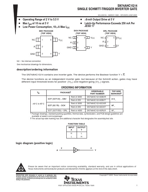
sn74ahc1g14单路施密特触发反向器
PACKAGING INFORMATIONOrderable Device Status (1)Package Type PackageDrawing Pins Package Qty Eco Plan (2)Lead/Ball FinishMSL Peak Temp (3)Samples(Requires Login)SN74AHC1G14DBVR ACTIVE SOT-23DBV53000Green (RoHS& no Sb/Br)CU NIPDAU Level-1-260C-UNLIMSN74AHC1G14DBVRE4ACTIVE SOT-23DBV53000Green (RoHS& no Sb/Br)CU NIPDAU Level-1-260C-UNLIMSN74AHC1G14DBVRG4ACTIVE SOT-23DBV53000Green (RoHS& no Sb/Br)CU NIPDAU Level-1-260C-UNLIMSN74AHC1G14DBVT ACTIVE SOT-23DBV5250Green (RoHS& no Sb/Br)CU NIPDAU Level-1-260C-UNLIMSN74AHC1G14DBVTE4ACTIVE SOT-23DBV5250Green (RoHS& no Sb/Br)CU NIPDAU Level-1-260C-UNLIMSN74AHC1G14DBVTG4ACTIVE SOT-23DBV5250Green (RoHS& no Sb/Br)CU NIPDAU Level-1-260C-UNLIMSN74AHC1G14DCKR ACTIVE SC70DCK53000Green (RoHS& no Sb/Br)CU NIPDAU Level-1-260C-UNLIMSN74AHC1G14DCKRE4ACTIVE SC70DCK53000Green (RoHS& no Sb/Br)CU NIPDAU Level-1-260C-UNLIMSN74AHC1G14DCKRG4ACTIVE SC70DCK53000Green (RoHS& no Sb/Br)CU NIPDAU Level-1-260C-UNLIMSN74AHC1G14DCKT ACTIVE SC70DCK5250Green (RoHS& no Sb/Br)CU NIPDAU Level-1-260C-UNLIMSN74AHC1G14DCKTE4ACTIVE SC70DCK5250Green (RoHS& no Sb/Br)CU NIPDAU Level-1-260C-UNLIMSN74AHC1G14DCKTG4ACTIVE SC70DCK5250Green (RoHS& no Sb/Br)CU NIPDAU Level-1-260C-UNLIMSN74AHC1G14DRLR ACTIVE SOT DRL54000Green (RoHS& no Sb/Br)CU NIPDAU Level-1-260C-UNLIMSN74AHC1G14DRLRG4ACTIVE SOT DRL54000Green (RoHS& no Sb/Br)CU NIPDAU Level-1-260C-UNLIM(1) The marketing status values are defined as follows:ACTIVE: Product device recommended for new designs.LIFEBUY: TI has announced that the device will be discontinued, and a lifetime-buy period is in effect.NRND: Not recommended for new designs. Device is in production to support existing customers, but TI does not recommend using this part in a new design. PREVIEW: Device has been announced but is not in production. Samples may or may not be available.OBSOLETE: TI has discontinued the production of the device.Addendum-Page 1(2) Eco Plan - The planned eco-friendly classification: Pb-Free (RoHS), Pb-Free (RoHS Exempt), or Green (RoHS & no Sb/Br) - please check /productcontent for the latest availability information and additional product content details.TBD: The Pb-Free/Green conversion plan has not been defined.Pb-Free (RoHS): TI's terms "Lead-Free" or "Pb-Free" mean semiconductor products that are compatible with the current RoHS requirements for all 6 substances, including the requirement that lead not exceed 0.1% by weight in homogeneous materials. Where designed to be soldered at high temperatures, TI Pb-Free products are suitable for use in specified lead-free processes.Pb-Free (RoHS Exempt): This component has a RoHS exemption for either 1) lead-based flip-chip solder bumps used between the die and package, or 2) lead-based die adhesive used between the die and leadframe. The component is otherwise considered Pb-Free (RoHS compatible) as defined above.Green (RoHS & no Sb/Br): TI defines "Green" to mean Pb-Free (RoHS compatible), and free of Bromine (Br) and Antimony (Sb) based flame retardants (Br or Sb do not exceed 0.1% by weight in homogeneous material)(3) MSL, Peak Temp. -- The Moisture Sensitivity Level rating according to the JEDEC industry standard classifications, and peak solder temperature.Important Information and Disclaimer:The information provided on this page represents TI's knowledge and belief as of the date that it is provided. TI bases its knowledge and belief on information provided by third parties, and makes no representation or warranty as to the accuracy of such information. Efforts are underway to better integrate information from third parties. TI has taken and continues to take reasonable steps to provide representative and accurate information but may not have conducted destructive testing or chemical analysis on incoming materials and chemicals. TI and TI suppliers consider certain information to be proprietary, and thus CAS numbers and other limited information may not be available for release.In no event shall TI's liability arising out of such information exceed the total purchase price of the TI part(s) at issue in this document sold by TI to Customer on an annual basis.Addendum-Page 2TAPE AND REEL INFORMATION*All dimensions are nominal Device Package Type Package DrawingPinsSPQ Reel Diameter (mm)Reel Width W1(mm)A0(mm)B0(mm)K0(mm)P1(mm)W (mm)Pin1Quadrant SN74AHC1G14DBVR SOT-23DBV 53000178.09.0 3.23 3.17 1.37 4.08.0Q3SN74AHC1G14DBVR SOT-23DBV 53000178.09.2 3.3 3.2 1.55 4.08.0Q3SN74AHC1G14DBVR SOT-23DBV 53000180.09.2 3.17 3.23 1.37 4.08.0Q3SN74AHC1G14DBVT SOT-23DBV 5250178.09.0 3.23 3.17 1.37 4.08.0Q3SN74AHC1G14DBVT SOT-23DBV 5250180.09.2 3.17 3.23 1.37 4.08.0Q3SN74AHC1G14DBVT SOT-23DBV 5250178.09.2 3.3 3.2 1.55 4.08.0Q3SN74AHC1G14DCKR SC70DCK 53000180.09.2 2.3 2.55 1.2 4.08.0Q3SN74AHC1G14DCKR SC70DCK 53000178.09.2 2.4 2.4 1.22 4.08.0Q3SN74AHC1G14DCKR SC70DCK 53000178.09.0 2.4 2.5 1.2 4.08.0Q3SN74AHC1G14DCKT SC70DCK 5250178.09.0 2.4 2.5 1.2 4.08.0Q3SN74AHC1G14DCKT SC70DCK 5250180.09.2 2.3 2.55 1.2 4.08.0Q3SN74AHC1G14DCKT SC70DCK 5250178.09.2 2.4 2.4 1.22 4.08.0Q3SN74AHC1G14DRLR SOT DRL 54000180.08.4 1.98 1.780.69 4.08.0Q3*All dimensions are nominalDevice Package Type Package Drawing Pins SPQ Length(mm)Width(mm)Height(mm) SN74AHC1G14DBVR SOT-23DBV53000180.0180.018.0 SN74AHC1G14DBVR SOT-23DBV53000180.0180.018.0 SN74AHC1G14DBVR SOT-23DBV53000205.0200.033.0 SN74AHC1G14DBVT SOT-23DBV5250180.0180.018.0 SN74AHC1G14DBVT SOT-23DBV5250205.0200.033.0 SN74AHC1G14DBVT SOT-23DBV5250180.0180.018.0 SN74AHC1G14DCKR SC70DCK53000205.0200.033.0 SN74AHC1G14DCKR SC70DCK53000180.0180.018.0 SN74AHC1G14DCKR SC70DCK53000180.0180.018.0 SN74AHC1G14DCKT SC70DCK5250180.0180.018.0 SN74AHC1G14DCKT SC70DCK5250205.0200.033.0 SN74AHC1G14DCKT SC70DCK5250180.0180.018.0SN74AHC1G14DRLR SOT DRL54000202.0201.028.0IMPORTANT NOTICETexas Instruments Incorporated and its subsidiaries(TI)reserve the right to make corrections,modifications,enhancements,improvements, and other changes to its products and services at any time and to discontinue any product or service without notice.Customers should obtain the latest relevant information before placing orders and should verify that such information is current and complete.All products are sold subject to TI’s terms and conditions of sale supplied at the time of order acknowledgment.TI warrants performance of its hardware products to the specifications applicable at the time of sale in accordance with TI’s standard warranty.Testing and other quality control techniques are used to the extent TI deems necessary to support this warranty.Except where mandated by government requirements,testing of all parameters of each product is not necessarily performed.TI assumes no liability for applications assistance or customer product design.Customers are responsible for their products and applications using TI components.To minimize the risks associated with customer products and applications,customers should provide adequate design and operating safeguards.TI does not warrant or represent that any license,either express or implied,is granted under any TI patent right,copyright,mask work right, or other TI intellectual property right relating to any combination,machine,or process in which TI products or services are rmation published by TI regarding third-party products or services does not constitute a license from TI to use such products or services or a warranty or endorsement e of such information may require a license from a third party under the patents or other intellectual property of the third party,or a license from TI under the patents or other intellectual property of TI.Reproduction of TI information in TI data books or data sheets is permissible only if reproduction is without alteration and is accompanied by all associated warranties,conditions,limitations,and notices.Reproduction of this information with alteration is an unfair and deceptive business practice.TI is not responsible or liable for such altered rmation of third parties may be subject to additional restrictions.Resale of TI products or services with statements different from or beyond the parameters stated by TI for that product or service voids all express and any implied warranties for the associated TI product or service and is an unfair and deceptive business practice.TI is not responsible or liable for any such statements.TI products are not authorized for use in safety-critical applications(such as life support)where a failure of the TI product would reasonably be expected to cause severe personal injury or death,unless officers of the parties have executed an agreement specifically governing such use.Buyers represent that they have all necessary expertise in the safety and regulatory ramifications of their applications,and acknowledge and agree that they are solely responsible for all legal,regulatory and safety-related requirements concerning their products and any use of TI products in such safety-critical applications,notwithstanding any applications-related information or support that may be provided by TI.Further,Buyers must fully indemnify TI and its representatives against any damages arising out of the use of TI products in such safety-critical applications.TI products are neither designed nor intended for use in military/aerospace applications or environments unless the TI products are specifically designated by TI as military-grade or"enhanced plastic."Only products designated by TI as military-grade meet military specifications.Buyers acknowledge and agree that any such use of TI products which TI has not designated as military-grade is solely at the Buyer's risk,and that they are solely responsible for compliance with all legal and regulatory requirements in connection with such use. TI products are neither designed nor intended for use in automotive applications or environments unless the specific TI products are designated by TI as compliant with ISO/TS16949requirements.Buyers acknowledge and agree that,if they use any non-designated products in automotive applications,TI will not be responsible for any failure to meet such requirements.Following are URLs where you can obtain information on other Texas Instruments products and application solutions:Products ApplicationsAudio /audio Automotive and Transportation /automotiveAmplifiers Communications and Telecom /communicationsData Converters Computers and Peripherals /computersDLP®Products Consumer Electronics /consumer-appsDSP Energy and Lighting /energyClocks and Timers /clocks Industrial /industrialInterface Medical /medicalLogic Security /securityPower Mgmt Space,Avionics and Defense /space-avionics-defense Microcontrollers Video and Imaging /videoRFID OMAP Mobile Processors /omapWireless Connectivity /wirelessconnectivityTI E2E Community Home Page Mailing Address:Texas Instruments,Post Office Box655303,Dallas,Texas75265Copyright©2012,Texas Instruments Incorporated。
74AC14 六角施密特触发器
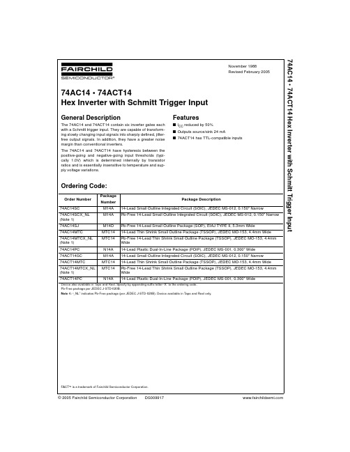
© 2005 Fairchild Semiconductor Corporation DS009917November 1988Revised February 200574AC14 • 74ACT14 Hex Inverter with Schmitt Trigger Input74AC14 • 74ACT14Hex Inverter with Schmitt Trigger InputGeneral DescriptionThe 74AC14 and 74ACT14 contain six inverter gates each with a Schmitt trigger input. They are capable of transform-ing slowly changing input signals into sharply defined, jitter-free output signals. In addition, they have a greater noise margin than conventional inverters.The 74AC14 and 74ACT14 have hysteresis between the positive-going and negative-going input thresholds (typi-cally 1.0V) which is determined internally by transistor ratios and is essentially insensitive to temperature and sup-ply voltage variations.Featuress I CC reduced by 50%s Outputs source/sink 24 mAs 74ACT14 has TTL-compatible inputsOrdering Code:Device also available in Tape and Reel. Specify by appending suffix letter “X” to the ordering code.Pb-Free package per JEDEC J-STD-020B.Note 1: “_NL” indicates Pb-Free package (per JEDEC J-STD-020B). Device available in Tape and Reel only.FACT ¥ is a trademark of Fairchild Semiconductor Corporation.Order Number Package Package DescriptionNumber 74AC14SC M14A 14-Lead Small Outline Integrated Circuit (SOIC), JEDEC MS-012, 0.150" Narrow 74AC14SCX_NL (Note 1)M14A Pb-Free 14-Lead Small Outline Integrated Circuit (SOIC), JEDEC MS-012, 0.150" Narrow 74AC14SJ M14D Pb-Free 14-Lead Small Outline Package (SOP), EIAJ TYPE II, 5.3mm Wide74AC14MTC MTC1414-Lead Thin Shrink Small Outline Package (TSSOP), JEDEC MO-153, 4.4mm Wide 74AC14MTCX_NL (Note 1)MTC14Pb-Free 14-Lead Thin Shrink Small Outline Package (TSSOP), JEDEC MO-153, 4.4mm Wide74AC14PC N14A 14-Lead Plastic Dual-In-Line Package (PDIP), JEDEC MS-001, 0.300" Wide 74ACT14SC M14A 14-Lead Small Outline Integrated Circuit (SOIC), JEDEC MS-012, 0.150" Narrow 74ACT14MTC MTC1414-Lead Thin Shrink Small Outline Package (TSSOP), JEDEC MO-153, 4.4mm Wide 74ACT14MTCX_NL (Note 1)MTC14Pb-Free 14-Lead Thin Shrink Small Outline Package (TSSOP), JEDEC MO-153, 4.4mm Wide74ACT14PCN14A14-Lead Plastic Dual-In-Line Package (PDIP), JEDEC MS-001, 0.300" Wide 274A C 14 • 74A C T 14Logic SymbolIEEE/IECPin DescriptionsConnection DiagramFunction TablePin Names Description I n Inputs O nOutputsInput Output A O L H HL74AC14 • 74ACT14Absolute Maximum Ratings (Note 2)Recommended Operating ConditionsNote 2: Absolute maximum ratings are those values beyond which damage to the device may occur. The databook specifications should be met, with-out exception, to ensure that the system design is reliable over its power supply, temperature, and output/input loading variables. Fairchild does not recommend operation of FACT ¥ circuits outside databook specifications.DC Electrical Characteristics for ACNote 3: All outputs loaded; thresholds on input associated with output under test.Note 4: Maximum test duration 2.0 ms, one output loaded at a time.Note 5: I IN and I CC @ 3.0V are guaranteed to be less than or equal to the respective limit @ 5.5V V CC .Supply Voltage (V CC ) 0.5V to 7.0VDC Input Diode Current (I IK )V I 0.5V 20 mA V I V CC 0.5V 20 mADC Input Voltage (V I )0.5V to V CC 0.5VDC Output Diode Current (I OK )V O 0.5V 20 mA V O V CC 0.5V 20 mADC Output Voltage (V O ) 0.5V to V CC 0.5VDC Output Source or Sink Current (I O )r 50 mA DC V CC or Ground Current per Output Pin (I CC or I GND )r 50 mAStorage Temperature (T STG ) 65q C to 150q CJunction Temperature (T J )PDIP140q CSupply Voltage (V CC )AC 2.0V to 6.0V ACT4.5V to5.5V Input Voltage (V I )0V to V CC Output Voltage (V O )0V toV CCOperating Temperature (T A )40q C to 85q CSymbol ParameterV CC T A 25q C T A 40q C to 85q C UnitsConditions(V)Typ Guaranteed LimitsV OHMinimum HIGH Level 3.0 2.99 2.9 2.9V I OUT 50 P AOutput Voltage4.5 4.49 4.4 4.45.5 5.495.4 5.43.0 2.56 2.46V I OH 124.5 3.86 3.76I OH 24 mA5.54.86 4.76I OH 24 mA (Note 3)V OLMaximum LOW Level 3.00.0020.10.1VI OUT 50 P AOutput Voltage4.50.0010.10.15.50.0010.10.13.00.360.44VI OL 124.50.360.44I OL 24 mA5.50.360.44I OL 24 mA (Note 3)I IN (Note 5)Maximum Input Leakage Current 5.5r 0.1r 1.0P A V I V CC , GND V tMaximum Positive 3.0 2.2 2.2T A Worst CaseThreshold4.5 3.2 3.2V5.5 3.9 3.9V tMinimum Negative 3.00.50.5T A Worst CaseThreshold4.50.90.9V5.5 1.1 1.1V H(MAX)Maximum Hysteresis3.0 1.2 1.2T A Worst Case4.5 1.4 1.4V5.51.6 1.6V H(MIN)Minimum Hysteresis3.00.30.3T A Worst Case4.50.40.4V5.50.50.5I OLD Minimum Dynamic 5.575mA V OLD 1.65V Max I OHD Output Current (Note 4) 5.5 75mA V OHD 3.85V Min I CC Maximum Quiescent 5.52.020.0P AV IN V CC (Note 5)Supply Currentor GND 474A C 14 • 74A C T 14AC Electrical Characteristics for ACNote 6: Voltage Range 3.3 is 3.3V r 0.3VVoltage Range 5.0 is 5.0V r 0.5VDC Electrical Characteristics for ACTNote 7: All outputs loaded; thresholds on input associated with output under test.Note 8: Maximum test duration 2.0 ms, one output loaded at a time.Symbol ParameterV CCT A 25q C T A 40q C to 85q CUnits(V)C L 50 pFC L 50 pF (Note 6)Min Typ Max Min Max t PLH Propagation Delay 3.3 1.59.513.5 1.515.0ns 5.0 1.57.010.0 1.511.0t PHLPropagation Delay3.3 1.57.511.5 1.513.0ns 5.01.56.08.51.59.5Symbol ParameterV CC T A 25q C T A 40q C to 85q C Units Conditions(V)Typ Guaranteed LimitsV IH Minimum HIGH Level 4.5 1.5 2.0 2.0V V OUT 0.1V Input Voltage5.5 1.5 2.0 2.0or V CC 0.1V V IL Maximum LOW Level 4.5 1.50.80.8V V OUT 0.1V Output Voltage 5.5 1.50.80.8or V CC 0.1V V OHMinimum HIGH Level 4.5 4.49434 4.4VI OUT 50P A Output Voltage5.5 5.495.4 5.4VV IN V IL or V IH4.5 3.86 3.76I OH 24 mA5.54.864.76I OH 24 mA (Note 7)V OLMaximum LOW Level 4.50.0010.10.1VI OUT 50 P A Output Voltage5.50.0010.10.1V V IN V IL or V IH4.50.360.44I OL 24 mA5.50.360.44I OL 24 mA (Note 7)I IN Maximum Input Leakage Current 5.5r 0.1r 1.0P A V I V CC , GND V H(MAX)Maximum Hysteresis 4.5 1.4 1.4V T A Worst Case 5.5 1.6 1.6V H(MIN)Minimum Hysteresis 4.50.40.4V T A Worst Case 5.50.50.5V t Maximum Positive 4.5 2.0 2.0V T A Worst Case Threshold 5.5 2.0 2.0V t Minimum Negative 4.50.80.8V T A Worst Case Threshold5.50.80.8I CCT Maximum I CC /Input 5.50.61.5mA V I V CC2.1V I OLD Minimum Dynamic 5.575mA V OLD 1.65V Max I OHD Output Current (Note 8) 5.5 75mA V OHD 3.85V Min I CCMaximum Quiescent 5.52.020.0P AV IN V CC Supply Currentor GND74AC14 • 74ACT14AC Electrical Characteristics for ACTNote 9: Voltage Range 5.0 is 5.0V r 0.5VCapacitanceSymbol Parameter V CCT A 25q C T A 40q C to 85q CUnits(V)C L 50 pFC L 50 pF (Note 9)Min Typ Max Min Max t PLH Propagation Delay 5.0 3.08.010.0 3.011.0ns Data to Output t PHLPropagation Delay 5.03.08.010.03.011.0ns Data to OutputSymbol ParameterTyp Units ConditionsC IN Input Capacitance4.5pF V CC OPEN C PDPower Dissipation Capacitance for AC25.0pFV CC 5.0Vfor ACT80 674A C 14 • 74A C T 14Physical Dimensions inches (millimeters) unless otherwise noted14-Lead Small Outline Integrated Circuit (SOIC), JEDEC MS-012, 0.150" NarrowPackage Number M14A74AC14 • 74ACT14Physical Dimensionsinches (millimeters) unless otherwise noted (Continued)Pb-Free 14-Lead Small Outline Package (SOP), EIAJ TYPE II, 5.3mm WidePackage Number M14D 874A C 14 • 74A C T 14Physical Dimensions inches (millimeters) unless otherwise noted (Continued)14-Lead Thin Shrink Small Outline Package (TSSOP), JEDEC MO-153, 4.4mm WidePackage Number MTC14974AC14 • 74ACT14 Hex Inverter with Schmitt Trigger InputPhysical Dimensions inches (millimeters) unless otherwise noted (Continued)14-Lead Plastic Dual-In-Line Package (PDIP), JEDEC MS-001, 0.300" WidePackage Number N14AFairchild does not assume any responsibility for use of any circuitry described, no circuit patent licenses are implied and Fairchild reserves the right at any time without notice to change said circuitry and specifications.LIFE SUPPORT POLICYFAIRCHILD ’S PRODUCTS ARE NOT AUTHORIZED FOR USE AS CRITICAL COMPONENTS IN LIFE SUPPORT DEVICES OR SYSTEMS WITHOUT THE EXPRESS WRITTEN APPROVAL OF THE PRESIDENT OF FAIRCHILD SEMICONDUCTOR CORPORATION. As used herein:1.Life support devices or systems are devices or systems which, (a) are intended for surgical implant into the body, or (b) support or sustain life, and (c) whose failure to perform when properly used in accordance with instructions for use provided in the labeling, can be rea-sonably expected to result in a significant injury to the user.2. A critical component in any component of a life support device or system whose failure to perform can be rea-sonably expected to cause the failure of the life support device or system, or to affect its safety or effectiveness.。
74HC14中文资料

74HC14的作用:六反相斯密特触发器74HC14引脚图:图1 引脚功能74HC14真值表:Input输入output输出A YL HH L74HC14电气参数:极限参数:Switching Characteristics开关特性at VCC = 5V and TA = 25℃采用施密特触发器74HC14的光耦接收整形电路:图2 光电耦合器接收整形电路采用施密特触发器74HC14的方波振荡器电路图3 方波振荡器ST188反射式红外光电传感器使用方法一、特点1.采用高发射功率红外光电二极管和高灵敏度光电晶体管组成。
2.检测距离可调整范围大,4-13mm 可用。
3.采用非接触检测方式。
二、外形尺寸左图右图左边是光电二极管的外形图,由发射二极管和接收管组成,如右图的电路示意图。
A、K是红外发射二极管的正负极,C、E是接收管的正负极。
因此只要A极接高电平、K极接低电平,红外发射管就能发出红外线。
可以在传感器加上外围电路来检测接收管的信号,进而确定是否接受到反射回来的红外线。
如下图右下方的器件工作示意图。
三、常用电路根据反射式红外光电传感器的原理和内部结构,我们可以设计上面的电路,电阻主要起限流作用,电阻值常设置为:R1=510Ω,R2=20kΩ。
这样,如果接收管接收到反射回来的红外线,红外接收头导通,E管脚输出高电平,接近Vcc;如果没有没有接收到反射回来的红外线,红外接收头不导通,E管脚输出低电平,接近GND。
在实际应用中,我们可以通过单片机扫描E管脚(类似按键扫描的方法)以确定接收管的状态。
四、智能车中黑白线应用白色物质吸收光线少,大部分光波被反射;黑色物质能够吸收大部分光波,只反射部分光波。
利用这一点,我们选取合适的测量距离,如1cm(最佳的测量高度可以根据多次实验结果比较调节)。
结合上面的应用电路,这样可以通过检测E脚的值(0/1)确定传感器下面是白色还是黑色,达到判断的目的。
74LS14反向器实验

74LS14反向器实验
74LS14 是一个6反向器,引脚定义如图:A端为输入端,Y端为输出端,一片芯片一共6路,即1,3,5,9,11,13 为输入端, 2,4,6,8,10,12 为输出端,输出结果与输入结果反向。
即如果输入端为高电平,那么输出为低电平。
如果输入低电平,输出为高电平。
在本套件中,一共使用了2片74LS14芯片,组成8路反向器。
反向器是重要的数字电路之一,下面我带领大家来学习反向器的应用。
实验目的:先做一个8路加法器的实验,然后通过反向器后,观察LE D的发光管的状态变化。
相关原理:
程序运行照片:
1、直接连接:用一条8PIN的数据排线把CP U部份的P1口(JP44)连接到八路指示灯部份的JP32
2、通过反向器连接:用一条8PIN的数据排线把CP U部份的P1口(JP44)接到反向器部份的输入端JP29用一条8PI N的数据排线把反向器的输出端JP34接到八路指示灯部份的JP32程序流程图:
汇编语言参考程序:
org 0000h
ajmp main
org 0080h
main: mov a,#0
loop: mov p1,a ;输出到P1口call delay ;延时。
inc a ;每次加1
jmp loop
delay: mov r5,#50 ;延时。
d1: mov r6,#40
d2: mov r7,#248 djnz r7,$
djnz r6,d2
djnz r5,d1
ret
end。
74HC14中文资料

74HC14引脚图:
图1 引脚功能
74HC14真值表:
74HC14电气参数:
极限参数:
Switching Characteristics开关特性 at VCC = 5V and TA = 25℃
采用施密特触发器74HC14的光耦接收整形电路:
图2 光电耦合器接收整形电路
采用施密特触发器74HC14的方波振荡器电路
图3 方波振荡器
施密特触发器.主要用要将上下沿较缓或奇变较大的的数字信号变为方波形式以利数字信号接收电路识别.比如一串高频数字信号方波经过一个并普通光耦后波形可能奇变的后级不能识别,加一个74HC14进行整形
编辑本段74HC14概述:
74HC14是一款高速CMOS器件,74HC14引脚兼容低功耗肖特基TTL (LSTTL)系列。
74HC14遵循JEDEC标准。
74HC14实现了6路施密特触发反相器,可将缓慢变化的输入信号转换成清晰、无抖动的输出信号。
编辑本段特性:
应用:波形、脉冲整形器
非稳态多谐振荡器
单稳多谐振荡器
兼容JEDEC标准
ESD保护:
HBM EIA/JESD22-A114-A超过2000 V
MM EIA/JESD22-A115-A超过200 V
温度范围 -40~+85 ℃ -40~+125 ℃
编辑本段主要参数:
典型电源电压:
正向输入阀值电压:VT+=
负向输入阀值电压:VT-=
驱动电流: +/
传输延迟:12ns @5V
逻辑电平:CMOS
引脚:14
封装类型:DIP。
74HC04和74HC14的区别(施密特触发的作用)[大全五篇]
![74HC04和74HC14的区别(施密特触发的作用)[大全五篇]](https://img.taocdn.com/s3/m/8e0c3d8bf021dd36a32d7375a417866fb84ac00c.png)
74HC04和74HC14的区别(施密特触发的作用)[大全五篇]第一篇:74HC04和74HC14的区别(施密特触发的作用)74HC04和74HC14的具体区别详解同样具有反相器功能,你知道74HC04和74HC14的具体区别吗?对于74HC04很好理解,输入低电平,输出高电平;输入高电平,输出低电平。
可是具体到几伏电压算高电平,几伏算低电平呢?答案是看手册。
下图是TI的74HC04的输入特性表,举个例子来看,当芯片供电电压Vcc=4.5V时,输入端最少输入3.15V电压才可以被74HC04识别为高电平;同理,输入端只有输入不大于1.35V的电压,才可以被识别为低电平。
下图是74HC04的输出特性表,在TEST CONDITIONS(测试条件)分别选IOH=-4mA和IOL=4mA,再举例子看,同上面的一样,当芯片供电电压Vcc=4.5V时,且输入端被识别为低电平,输出端VOH就是高电平,且最小值为3.84V;同理,当芯片供电电压Vcc=4.5V时,且输入端被识别为高电平,输出端VOL就是低电平,且最大值为0.33V。
从以上的分析可以看出,经74HC04的反相,到底输出几伏的高电平或低电平主要和该芯片的供电电压关系密切!以上对于74HC04的分析同样适用于74HC14!关于以上的数据,他们在手册中完全一样!也就是单纯作为反相器使用时,可以通用。
但是74HC14除了反相器这个基本功能外,他还是个施密特触发器。
关于什么是施密特触发器,现用一个图简单介绍:对于74HC14来说,当输入VI大于阀值电压VT+时,输出VO由高电平变低电平;当输入VI小于阀值电压VT-时,输出VO由低电平变高电平;通过上面分析,我们了解了施密特触发器是以反相器为基础的,以及阀值电压的基本概念。
下面来看一下74HC14这个施密特触发器的手册数据:VOH和VOL上文已经介绍过了,下面看一下VT+和VT-:当芯片供电电压Vcc=4.5V时,正向阀值的典型值VT+=2.5V,负向阀值的典型值VT-=1.6V。
74HC系列通用逻辑电路功能表

74HC00 TTL 2输入端四与非门74HC01 TTL 集电极开路2输入端四与非门74HC02 TTL 2输入端四或非门74HC03 TTL 集电极开路2输入端四与非门74HC04 TTL 六反相器74HC05 TTL 集电极开路六反相器74HC06 TTL 集电极开路六反相高压驱动器74HC07 TTL 集电极开路六正相高压驱动器74HC08 TTL 2输入端四与门74HC09 TTL 集电极开路2输入端四与门74HC10 TTL 3输入端3与非门74HC107 TTL 带清除主从双J-K触发器74HC109 TTL 带预置清除正触发双J-K触发器74HC11 TTL 3输入端3与门74HC112 TTL 带预置清除负触发双J-K触发器74HC12 TTL 开路输出3输入端三与非门74HC121 TTL 单稳态多谐振荡器74HC122 TTL 可再触发单稳态多谐振荡器74HC123 TTL 双可再触发单稳态多谐振荡器74HC125 TTL 三态输出高有效四总线缓冲门74HC126 TTL 三态输出低有效四总线缓冲门74HC13 TTL 4输入端双与非施密特触发器74HC132 TTL 2输入端四与非施密特触发器74HC133 TTL 13输入端与非门74HC136 TTL 四异或门74HC138 TTL 3-8线译码器/复工器74HC139 TTL 双2-4线译码器/复工器74HC14 TTL 六反相施密特触发器74HC145 TTL BCD—十进制译码/驱动器74HC15 TTL 开路输出3输入端三与门74HC150 TTL 16选1数据选择/多路开关74HC151 TTL 8选1数据选择器74HC153 TTL 双4选1数据选择器74HC154 TTL 4线—16线译码器74HC155 TTL 图腾柱输出译码器/分配器74HC156 TTL 开路输出译码器/分配器74HC157 TTL 同相输出四2选1数据选择器74HC158 TTL 反相输出四2选1数据选择器74HC16 TTL 开路输出六反相缓冲/驱动器74HC160 TTL 可预置BCD异步清除计数器74HC161 TTL 可予制四位二进制异步清除计数器74HC162 TTL 可预置BCD同步清除计数器74HC163 TTL 可予制四位二进制同步清除计数器74HC164 TTL 八位串行入/并行输出移位寄存器74HC165 TTL 八位并行入/串行输出移位寄存器74HC169 TTL 二进制四位加/减同步计数器74HC17 TTL 开路输出六同相缓冲/驱动器74HC170 TTL 开路输出4×4寄存器堆74HC173 TTL 三态输出四位D型寄存器74HC174HC TTL 带公共时钟和复位六D触发器74HC175 TTL 带公共时钟和复位四D触发器74HC180 TTL 9位奇数/偶数发生器/校验器74HC181 TTL 算术逻辑单元/函数发生器74HC185 TTL 二进制—BCD代码转换器74HC190 TTL BCD同步加/减计数器74HC191 TTL 二进制同步可逆计数器74HC192 TTL 可预置BCD双时钟可逆计数器74HC193 TTL 可预置四位二进制双时钟可逆计数器74HC194 TTL 四位双向通用移位寄存器74HC196 TTL 十进制/二-十进制可预置计数锁存器74HC197 TTL 二进制可预置锁存器/计数器74HC20 TTL 4输入端双与非门74HC21 TTL 4输入端双与门74HC22 TTL 开路输出4输入端双与非门74HC221 TTL 双/单稳态多谐振荡器74HC240 TTL 八反相三态缓冲器/线驱动器74HC241 TTL 八同相三态缓冲器/线驱动器74HC243 TTL 四同相三态总线收发器74HC244 TTL 八同相三态缓冲器/线驱动器74HC245 TTL 八同相三态总线收发器74HC247 TTL BCD—7段15V输出译码/驱动器74HC248 TTL BCD—7段译码/升压输出驱动器74HC249 TTL BCD—7段译码/开路输出驱动器74HC251 TTL 三态输出8选1数据选择器/复工器74HC253 TTL 三态输出双4选1数据选择器/复工器74HC256 TTL 双四位可寻址锁存器74HC257 TTL 三态原码四2选1数据选择器/复工器74HC258 TTL 三态反码四2选1数据选择器/复工器74HC259 TTL 八位可寻址锁存器/3-8线译码器74HC26 TTL 2输入端高压接口四与非门74HC260 TTL 5输入端双或非门74HC266 TTL 2输入端四异或非门74HC27 TTL 3输入端三或非门74HC273 TTL 带公共时钟复位八D触发器74HC279 TTL 四图腾柱输出S-R锁存器74HC28 TTL 2输入端四或非门缓冲器74HC283 TTL 4位二进制全加器74HC290 TTL 二/五分频十进制计数器74HC293 TTL 二/八分频四位二进制计数器74HC295 TTL 四位双向通用移位寄存器74HC298 TTL 四2输入多路带存贮开关74HC299 TTL 三态输出八位通用移位寄存器74HC30 TTL 8输入端与非门74HC32 TTL 2输入端四或门74HC322 TTL 带符号扩展端八位移位寄存器74HC323 TTL 三态输出八位双向移位/存贮寄存器74HC33 TTL 开路输出2输入端四或非缓冲器74HC347 TTL BCD—7段译码器/驱动器74HC352 TTL 双4选1数据选择器/复工器74HC353 TTL 三态输出双4选1数据选择器/复工器74HC365 TTL 门使能输入三态输出六同相线驱动器74HC365 TTL 门使能输入三态输出六同相线驱动器74HC366 TTL 门使能输入三态输出六反相线驱动器74HC367 TTL 4/2线使能输入三态六同相线驱动器74HC368 TTL 4/2线使能输入三态六反相线驱动器74HC37 TTL 开路输出2输入端四与非缓冲器74HC373 TTL 三态同相八D锁存器74HC374 TTL 三态反相八D锁存器74HC375 TTL 4位双稳态锁存器74HC377 TTL 单边输出公共使能八D锁存器74HC378 TTL 单边输出公共使能六D锁存器74HC379 TTL 双边输出公共使能四D锁存器74HC38 TTL 开路输出2输入端四与非缓冲器74HC380 TTL 多功能八进制寄存器74HC39 TTL 开路输出2输入端四与非缓冲器74HC390 TTL 双十进制计数器74HC393 TTL 双四位二进制计数器74HC40 TTL 4输入端双与非缓冲器74HC42 TTL BCD—十进制代码转换器74HC352 TTL 双4选1数据选择器/复工器74HC353 TTL 三态输出双4选1数据选择器/复工器74HC365 TTL 门使能输入三态输出六同相线驱动器74HC366 TTL 门使能输入三态输出六反相线驱动器74HC367 TTL 4/2线使能输入三态六同相线驱动器74HC368 TTL 4/2线使能输入三态六反相线驱动器74HC37 TTL 开路输出2输入端四与非缓冲器74HC373 TTL 三态同相八D锁存器74HC374 TTL 三态反相八D锁存器74375 TTL 4位双稳态锁存器74377 TTL 单边输出公共使能八D锁存器74378 TTL 单边输出公共使能六D锁存器74379 TTL 双边输出公共使能四D锁存器7438 TTL 开路输出2输入端四与非缓冲器74380 TTL 多功能八进制寄存器7439 TTL 开路输出2输入端四与非缓冲器74390 TTL 双十进制计数器74393 TTL 双四位二进制计数器7440 TTL 4输入端双与非缓冲器7442 TTL BCD—十进制代码转换器74447 TTL BCD—7段译码器/驱动器7445 TTL BCD—十进制代码转换/驱动器74450 TTL 16:1多路转接复用器多工器74451 TTL 双8:1多路转接复用器多工器74453 TTL 四4:1多路转接复用器多工器7446 TTL BCD—7段低有效译码/驱动器74460 TTL 十位比较器74461 TTL 八进制计数器74465 TTL 三态同相2与使能端八总线缓冲器74466 TTL 三态反相2与使能八总线缓冲器74467 TTL 三态同相2使能端八总线缓冲器74468 TTL 三态反相2使能端八总线缓冲器74469 TTL 八位双向计数器7447 TTL BCD—7段高有效译码/驱动器7448 TTL BCD—7段译码器/内部上拉输出驱动74490 TTL 双十进制计数器74491 TTL 十位计数器74498 TTL 八进制移位寄存器7450 TTL 2-3/2-2输入端双与或非门74502 TTL 八位逐次逼近寄存器74503 TTL 八位逐次逼近寄存器7451 TTL 2-3/2-2输入端双与或非门74533 TTL 三态反相八D锁存器74534 TTL 三态反相八D锁存器7454 TTL 四路输入与或非门74540 TTL 八位三态反相输出总线缓冲器7455 TTL 4输入端二路输入与或非门74563 TTL 八位三态反相输出触发器74564 TTL 八位三态反相输出D触发器74573 TTL 八位三态输出触发器74574 TTL 八位三态输出D触发器74645 TTL 三态输出八同相总线传送接收器74670 TTL 三态输出4×4寄存器堆7473 TTL 带清除负触发双J-K触发器7474 TTL 带置位复位正触发双D触发器7476 TTL 带预置清除双J-K触发器7483 TTL 四位二进制快速进位全加器7485 TTL 四位数字比较器7486 TTL 2输入端四异或门7490 TTL 可二/五分频十进制计数器7493 TTL 可二/八分频二进制计数器7495 TTL 四位并行输入\输出移位寄存器7497 TTL 6位同步二进制乘法器注:同型号的74系列、74HC系列、74LS系列芯片,逻辑功能上是一样的。
详细施密特触发器74HC14的中文资料

详细施密特触发器74HC14的中文资料74HC14为一个六反相施密特触发器真值表:Y=AInput输入output输出AYLHHL74HC14的引脚图如下,其中Vcc(14脚)是电源正电压引脚,GND(7脚)是电源地引脚,一片74HC14上共有6个反相器通道,第1、3、5、9、11、13脚分别是通道1、2、3、4、5、6的输入脚,2、4、6、8、10、12脚分别是通道1、2、3、4、5、6的输入出脚。
建议操作条件符号参数最小典型最大单位电源电压为 4.7555.25VVT,正向输入阈值电压为1.41.61.9VVT,反向输入阈值电压为0.50.81VHYS,输入滞后0.40.8-VIOHHIGH 高电平输出电流---0.4mAIOLLOW,低电平输出电流--8mATAFree ,工作温度0-70℃Note 2:VCC = 5V.电气特性超过推荐的工作自由空气温度范围(除非另有说明),符号参数条件最小典型最大单位输入钳位电压VCC 为最小,II = -18mA---1.5VVOHHIGH输出高电平电压VCC 为最小,IOH为最大VIL=最大2.73.4-VVOLLOW Level输出低电平电压VCC = 最小,IOL = 最大-0.350.5--Output V oltage输出电压VIH = 最小---VVCC = 最小,IOL = 4mA-0.250.4IT,正向阈值输入电流VCC = 5V,VI = VT+--0.14-mAIT,反向阈值输入电流VCC = 5V,VI = VT---0.18-mAII,输入电流@最大输入电压VCC = 最大,VI = 7V--0.1mAIIHHIGH ,输入高电平电流VCC = 最大,VI = 2.7V--20μAIILLOW ,输入低电平电流VCC = 最大,VI = 0.4V---0.4mAIOSShort ,短路输出电流VCC = 最大(Note 4)-20--100mAICCH,电平输出电源电流VCC = 最大-8.616mAICCL,低电平输出电源电流VCC = 最大-1221mANote 3:VCC = 5V,TA = 25℃.Note 4:一次不应超过一个输出,持续时间不应超过一秒。
- 1、下载文档前请自行甄别文档内容的完整性,平台不提供额外的编辑、内容补充、找答案等附加服务。
- 2、"仅部分预览"的文档,不可在线预览部分如存在完整性等问题,可反馈申请退款(可完整预览的文档不适用该条件!)。
- 3、如文档侵犯您的权益,请联系客服反馈,我们会尽快为您处理(人工客服工作时间:9:00-18:30)。
8. Limiting values
Table 4. Limiting values In accordance with the Absolute Maximum Rating System (IEC 60134). Voltages are referenced to GND (ground = 0 V). Symbol VCC IIK IOK IO ICC IGND Tstg Ptot Parameter supply voltage input clamping current output clamping current output current supply current ground current storage temperature total power dissipation DIP14 package SO14, (T)SSOP14 and DHVQFN14 packages
Fig 5.
Pin configuration DHVQFN14
6.2 Pin description
Table 2. Symbol 1A to 6A 1Y to 6Y GND VCC Pin description Pin 1, 3, 5, 9, 11, 13 2, 4, 6, 8, 10, 12 7 14 Description data input 1 data output 1 ground (0 V) supply voltage
74HC_HCT14
All information provided in this document is subject to legal disclaimers.
© NXP B.V. 2012. All rights reserved.
Product data sheet
Rev. 6 — 19 September 2012
4. Ordering information
Table 1. Ordering information Package Temperature range 74HC14N 74HCT14N 74HC14D 74HCT14D 74HC14DB 74HCT14DB 74HC14PW 74HCT14PW 74HC14BQ 74HCT14BQ 40 C to +125 C DHVQFN14 40 C to +125 C TSSOP14 40 C to +125 C SSOP14 40 C to +125 C SO14 plastic small outline package; 14 leads; body width 3.9 mm plastic shrink small outline package; 14 leads; body width 5.3 mm plastic thin shrink small outline package; 14 leads; body width 4.4 mm SOT108-1 SOT337-1 SOT402-1 40 C to +125 C Name DIP14 Description plastic dual in-line package; 14 leads (300 mil) Version SOT27-1 Type number
plastic dual in-line compatible thermal enhanced very SOT762-1 thin quad flat package; no leads; 14 terminals; body 2.5 3 0.85 mm
5. Functional diagram
© NXP B.V. 2012. All rights reserved.
Product data sheet
Rev. 6 — 19 September 2012
3 of 21
NXP Semiconductors
74HC14; 74HCT14
Hex inverting Schmitt trigger
2 of 21
NXP Semiconductors
74HC14; 74HCT14
Hex inverting Schmitt trigger
6. Pinning information
6.1 Pinning
terminal 1 index area 1Y 1A 1Y 2A 2Y 3A 3Y GND 1 2 3 4 5 6 7
7. Functional description
Table 3. Input nA L H
[1] H = HIGH voltage level; L = LOW voltage level.
Function table[1] Output nY H L
74HC_HCT14
All information provided in this document is subject to legal disclaimers.
74HC14; 74HCT14
Hex inverting Schmitt trigger
Rev. 6 — 19 September 2012 Product data sheet
1. General description
The 74HC14; 74HCT14 is a high-speed Si-gate CMOS device and is pin compatible with Low-power Schottky TTL (LSTTL). It is specified in compliance with JEDEC standard No. 7A. The 74HC14; 74HCT14 provides six inverting buffers with Schmitt-trigger action. It is capable of transforming slowly changing input signals into sharply defined, jitter-free output signals.
3. Applications
Wave and pulse shapers Astable multivibrators Monostable multivibrators
NXP Semiconductors
74HC14; 74HCT14
Hex inverting Schmitt trigger
Unit V mA mA mA mA mA C mW mW
The input and output voltage ratings may be exceeded if the input and output current ratings are observed. For DIP14 package: Ptot derates linearly with 12 mW/K above 70 C. For SO14 package: Ptot derates linearly with 8 mW/K above 70 C. For (T)SSOP14 packages: Ptot derates linearly with 5.5 mW/K above 60 C. For DHVQFN14 packages: Ptot derates linearly with 4.5 mW/K above 60 C.
(1) The die substrate is attached to this pad using conductive die attach material. It cannot be used as a supply pin or input.
Fig 4.
Pin configuration DIP14, SO14 and (T)SSOP14
2. Features and benefits
Low-power dissipation ESD protection: HBM JESD22-A114F exceeds 2000 V MM JESD22-A115-A exceeds 200 V Multiple package options Specified from 40 C to +85 C and from 40 C to +125 C
4 of 21
NXP Semiconductors
74HC14; 74HCT14
Hex inverting Schmitt trigger
10. Static characteristics
Table 6. Static characteristics At recommended operating conditions; voltages are referenced to GND (ground = 0 V). Symbol Parameter Conditions Tamb = 25 C Min 74HC14 VOH HIGH-level output voltage VI = VT+ or VT IO = 20 A; VCC = 2.0 V IO = 20 A; VCC = 4.5 V IO = 20 A; VCC = 6.0 V IO = 4.0 mA; VCC = 4.5 V IO = 5.2 mA; VCC = 6.0 V VOL LOW-level output voltage VI = VT+ or VT IO = 20 A; VCC = 2.0 V IO = 20 A; VCC = 4.5 V IO = 20 A; VCC = 6.0 V IO = 4.0 mA; VCC = 4.5 V IO = 5.2 mA; VCC = 6.0 V II ICC CI 74HCT14 VOH HIGH-level output voltage VI = VT+ or VT; VCC = 4.5 V IO = 20 A IO = 4.0 mA VOL LOW-level output voltage VI = VT+ or VT; VCC = 4.5 V IO = 20 A; IO = 4.0 mA; II ICC ICC input leakage current supply current additional supply current VI = VCC or GND; VCC = 5.5 V VI = VCC or GND; IO = 0 A; VCC = 5.5 V per input pin; VI = VCC 2.1 V; other pins at VCC or GND; IO = 0 A; VCC = 4.5 V to 5.5 V 0 0.15 30 0.1 0.26 0.1 2.0 108 0.1 0.33 1.0 20 135 0.1 0.4 1.0 40 147 V V A A A 4.4 3.98 4.5 4.32 4.4 3.84 4.4 3.7 V V input leakage current supply current input capacitance VI = VCC or GND; VCC = 6.0 V VI = VCC or GND; IO = 0 A; VCC = 6.0 V 0 0 0 0.15 0.16 3.5 0.1 0.1 0.1 0.26 0.26 0.1 2.0 0.1 0.1 0.1 0.33 0.33 1.0 20 0.1 0.1 0.1 0.4 0.4 1.0 40 V V V V V A A pF 1.9 4.4 5.9 3.98 5.48 2.0 4.5 6.0 4.32 5.81 1.9 4.4 5.9 3.84 5.34 1.9 4.4 5.9 3.7 5.2 V V V V V Typ Max Tamb = 40 C to +85 C Min Max Tamb = 40 C to +125 C Min Max Unit