
LT1358CS8中文资料
LT1358/LT1359 Dual and Quad 25MHz, 600V/µs Op Amps
FEATURES
s s s s s s s s s s s s s s s
DESCRIPTIO
25MHz Gain Bandwidth 600V/µs Slew Rate 2.5mA Maximum Supply Current per Amplifier Unity-Gain Stable C-LoadTM Op Amp Drives All Capacitive Loads 8nV/√Hz Input Noise Voltage 600µV Maximum Input Offset Voltage 500nA Maximum Input Bias Current 120nA Maximum Input Offset Current 20V/mV Minimum DC Gain, RL=1k 115ns Settling Time to 0.1%, 10V Step 220ns Settling Time to 0.01%, 10V Step ±12.5V Minimum Output Swing into 500Ω ±3V Minimum Output Swing into 150Ω Specified at ± 2.5V, ±5V, and ±15V
TJMAX = 150°C, θJA = 190°C/ W
TOP VIEW
OUT A
1 2 3 4 5 6 7 8 B C A D
16 OUT D 15 –IN D 14 +IN D 13 V – 12 +IN C 11 –IN C 10 OUT C 9
NC
–IN A +IN A V+ +IN B –IN B
ABSOLUTE MAXIMUM RATINGS
Total Supply Voltage (V+ to V –) ............................... 36V Differential Input Voltage (Transient Only) (Note 2)................................... ±10V Input Voltage ............................................................ ±VS Output Short-Circuit Duration (Note 3) ............ Indefinite
IOS IB en in RIN CIN
Input Offset Current Input Bias Current Input Noise Voltage Input Noise Current Input Resistance Input Resistance Input Capacitance f = 10kHz f = 10kHz VCM = ±12V Differential
2
U
U
W
W W U
W
(Note 1)
Operating Temperature Range (Note 7) ...–40°C to 85°C Specified Temperature Range (Note 8) ....–40°C to 85°C Maximum Junction Temperature (See Below) Plastic Package ................................................ 150°C Storage Temperature Range ..................–65°C to 150°C Lead Temperature (Soldering, 10 sec).................. 300°C
OUT B NC
S PACKAGE 16-LEAD PLASTIC SO
TJMAX = 150°C, θJA = 150°C/ W
±2.5V to ±15V ±2.5V to ±15V ±15V ±15V ±15V
元器件交易网
LT1358/LT1359
ELECTRICAL CHARACTERISTICS
6pF DAC INPUTS 12 5k
–
565A-TYPE
+
0.1µF 5k
1/2 LT1358
VOUT
V V OS + IOS 5kΩ + OUT < 1LSB A VOL
1358/1359 TA01
( )
U
1358/1359 TA02
U
1
元器件交易网
LT1358/LT1359
TA = 25°C, VCM = 0V unless otherwise noted.
VSUPPLY ±15V ±5V ±2.5V ±2.5V to ±15V ±2.5V to ±15V MIN TYP 0.2 0.2 0.3 40 120 8 0.8 35 80 6 3 MAX 0.6 0.6 0.8 120 500 UNITS mV mV mV nA nA nV/√Hz pA/√Hz MΩ MΩ pF
TOP VIEW
OUT A
1 2 3 4 5 6 7 B C A D
14 OUT D 13 –IN D 12 +IN D 11 V – 10 +IN C 9 8
–IN C
OUT C
ORDER PART NUMBER LT1359CN
–IN A +IN A V+ +IN B –IN B
OUT B
N PACKAGE 14-LEAD PDIP
The LT1358/LT1359 are dual and quad low power high speed operational amplifiers with outstanding AC and DC performance. The amplifiers feature much lower supply current and higher slew rate than devices with comparable bandwidth. The circuit topology is a voltage feedback amplifier with matched high impedance inputs and the slewing performance of a current feedback amplifier. The high slew rate and single stage design provide excellent settling characteristics which make the circuit an ideal choice for data acquisition systems. Each output drives a 500Ω load to ±12.5V with ±15V supplies and a 150Ω load to ±3V on ± 5V supplies. The amplifiers are stable with any capacitive load making them useful in buffer applications. The LT1358/LT1359 are members of a family of fast, high performance amplifiers using this unique topology and employing Linear Technology Corporation’s advanced bipolar complementary processing. For a single amplifier version of the LT1358/LT1359 see the LT1357 data sheet. For higher bandwidth devices with higher supply currents see the LT1360 through LT1365 data sheets. For lower supply current amplifiers see the LT1354 and LT1355/ LT1356 data sheets. Singles, duals, and quads of each amplifier are available.
TJMAX = 150°C, θJA = 110°C/ W
Consult factory for Industrial and Military grade parts.
ELECTRICAL CHARACTERISTICS
SYMBOL VOS PARAMETER Input Offset Voltage CONDITIONS
SYMBOL PARAMETER Input Voltage Range + CONDITIONS
TA = 25°C, VCM = 0V unless otherwise noted.
VSUPPLY ± 15V ± 5V ± 2.5V ± 15V ± 5V ± 2.5V MIN 12.0 2.5 0.5 TYP 13.4 3.5 1.1 –13.2 –12.0 –3.3 –2.5 –0.9 –0.5 83 78 68 92 ± 15V ± 15V ± 5V ± 5V ± 5V ± 2.5V ± 15V ± 15V ± 5V ± 5V ± 2.5V ± 15V ± 5V ± 15V ± 15V ± 5V ± 15V ± 5V ± 15V ± 5V ± 2.5V ± 15V ± 5V ± 15V ± 5V ± 15V ± 5V ± 15V ± 15V ± 5V ± 5V ± 15V ± 5V ± 15V ± 5V ± 15V ± 15V ± 15V ± 5V 100 18 15 20 7 20 7 1.5 7 13.3 12.5 3.5 3.0 1.3 25 20 30 300 150 97 84 75 106 65 25 45 25 6 30 13.8 13.0 4.0 3.3 1.7 30 25 42 600 220 9.6 11.7 25 22 20 8 9 27 27 9 11 115 220 110 380 0.1 0.1 0.50 0.35 0.3 113 2.0 1.9 2.5 2.4 MAX UNITS V V V V V V dB dB dB dB V/mV V/mV V/mV V/mV V/mV V/mV ±V ±V ±V ±V ±V mA mA mA V/µs V/µs MHz MHz MHz MHz MHz ns ns % % ns ns ns ns ns ns % % Deg Deg Ω dB mA mA
LTC1485IS8资料

1D UESCRIPTIOSFEATURE U A OPPLICATITYPICAL DIRORODI5V The LTC ®1485 is a low power differential bus/line trans-ceiver designed for multipoint data transmission standard RS485 applications with extended common-mode range (12V to –7V). It also meets the requirements of RS422.The CMOS with Schottky design offers significant power savings over its bipolar counterpart without sacrificing ruggedness against overload or ESD damage.The driver and receiver feature three-state outputs, with the driver outputs maintaining high impedance over the entire common-mode range. Excessive power dissipation caused by bus contention or faults is prevented by a thermal shutdown circuit which forces the driver outputs into a high impedance state. I/O pins are protected against multiple ESD strikes of over ±10kV.The receiver has a fail-safe feature which guarantees a high output state when the inputs are left open.Both AC and DC specifications are guaranteed from –40°C to 85°C and 4.75V to 5.25V supply voltage range.s Low Power RS485/RS422 Transceiver sLevel TranslatorU SA OPPLICATIs ESD Protection over ±10kV s Low Power: I CC = 1.8mA Typs28ns Typical Driver Propagation Delays with 4ns Skews Designed for RS485 or RS422 Applications s Single 5V Supplys–7V to 12V Bus Common-Mode Range Permits ±7V Ground Difference Between Devices on the Bus s Thermal Shutdown Protections Power-Up/Down Glitch-Free Driver OutputssDriver Maintains High Impedance in Three-State or with the Power OffsCombined Impedance of a Driver Output and Receiver Allows up to 32 Transceivers on the Bus s 60mV Typical Input HysteresissPin Compatible with the SN75176A, DS75176A, and SN75LBC1762A U G WA W U W A R BSOLUTEXI TI S W U U PACKAGE/ORDER I FOR ATIO(Note 1)Supply Voltage (V CC ).............................................. 12V Control Input Voltages................... –0.5V to V CC + 0.5V Control Input Currents........................ –50mA to 50mA Driver Input Voltages..................... –0.5V to V CC + 0.5V Driver Input Currents.......................... –25mA to 25mA Driver Output Voltages ......................................... ±14V Receiver Input Voltages........................................ ±14V Receiver Output Voltages .............. –0.5V to V CC + 0.5V Operating Temperature RangeLTC1485C............................................... 0°C to 70°C LTC1485I .......................................... –40°C to 85°C Storage Temperature Range................ –65°C to 150°C Lead Temperature (Soldering, 10 sec.)................ 300°CSYMBOL PARAMETERCONDITIONS MINTYP MAX UNITSV OD1Differential Driver Output Voltage (Unloaded)I O = 0q 5V V OD2Differential Driver Output Voltage (With Load)R = 50Ω, (RS422)q 2V R = 27Ω, (RS485) (Figure 1)q 1.55V ∆V OD Change in Magnitude of Driver DifferentialR = 27Ω or R = 50Ω (Figure 1)q 0.2V Output Voltage for Complementary Output States V OC Driver Common-Mode Output VoltageR = 27Ω or R = 50Ω (Figure 1)q 3V ∆|V OC |Change in Magnitude of Driver Common-Mode R = 27Ω or R = 50Ω (Figure 1)q 0.2V Output Voltage for Complementary Output States V INH Input High Voltage DI, DE, RE q 2.0V V INL Input Low Voltage DI, DE, RE q 0.8V I IN1Input CurrentDI, DE, REq ±2µA I IN2Input Current (A, B)V CC = 0V or 5.25V, V IN = 12V q 1.0mA V CC = 0V or 5.25V, V IN = –7V q –0.8mA V TH Differential Input Threshold Voltage for Receiver –7V ≤ V CM ≤ 12V q –0.20.2V ∆V TH Receiver Input Hysteresis V CM = 0Vq 60mV V OH Receiver Output High Voltage I O = –4mA, V ID = 0.2V q 3.5V V OL Receiver Output Low VoltageI O = 4mA, V ID = –0.2Vq 0.4V I OZR Three-State Output Current at Receiver V CC = Max 0.4V ≤ V O ≤ 2.4V q ±1µA I CCSupply CurrentNo Load; DI = GND or V CC Outputs Enabled q 1.8 2.3mA Outputs Disabled q 1.72.3mA R IN Receiver Input Resistance–7V ≤ V CM ≤ 12V q 12k ΩI OSD1Driver Short-Circuit Current, V OUT = High V O = –7V q 250mA I OSD2Driver Short-Circuit Current, V OUT = Low V O = 10 V q 250mA I OSRReceiver Short-Circuit Current0V ≤ V O ≤ V CCq785mAV CC = 5V (Notes 2, 3), unless otherwise noted.ELECTRICAL C C HARA TERISTICSC D Consult factory for Military grade parts.3SYMBOL PARAMETERCONDITIONSMIN TYP MAX UNITSt PLH Driver Input to Output R DIFF = 54Ω, C L1 = C L2 = 100pF q 103050ns(Figures 2, 5)t PHL Driver Input to Output R DIFF = 54Ω, C L1 = C L2 = 100pF q 103050ns (Figures 2, 5)t SKEW Driver Output to Output R DIFF = 54Ω, C L1 = C L2 = 100pF q 410ns (Figures 2, 5)t r , t fDriver Rise or Fall TimeR DIFF = 54Ω, C L1 = C L2 = 100pF q 51525ns (Figures 2, 5)t ZH Driver Enable to Output High C L = 100pF (Figures 4, 6) S2 Closed q 4070ns t ZL Driver Enable to Output Low C L = 100pF (Figures 4, 6) S1 Closed q 4070ns t LZ Driver Disable Time from Low C L = 15pF (Figures 4, 6) S1 Closed q 4070ns t HZ Driver Disable Time from High C L = 15pF (Figures 4, 6) S2 Closedq 4070ns tPLH Receiver Input to Output R DIFF = 54Ω, C L1 = C L2 = 100pF (Figures 2, 7)q 152550ns t PHL Receiver Input to Output R DIFF = 54Ω, C L1 = C L2 = 100pF (Figures 2, 7)q 203055ns t SKEW | t PLH – t PHL |R DIFF = 54Ω, C L1 = C L2 = 100pF (Figures 2, 7)q 515ns Differential Receiver Skewt ZL Receiver Enable to Output Low C L = 15pF (Figures 3, 8) S1 Closedq 3045ns t ZH Receiver Enable to Output High C L = 15pF (Figures 3, 8) S2 Closed q 3045ns t LZ Receiver Disable from Low C L = 15pF (Figures 3, 8) S1 Closed q 3045ns t HZ Receiver Disable from HighC L = 15pF (Figures 3, 8) S2 Closedq3045nsS UG C C HARA TERISTICSWITCHI V CC = 5V (Notes 2, 3), unless otherwise noted.The q denotes specifications which apply over the operating temperature range.Note 1: Absolute Maximum Ratings are those values beyond which the safety of the device cannot be guaranteed.Note 2: All currents into device pins are positive. All currents out of device pins are negative. All voltages are referenced to device ground unless otherwise specified.Note 3: All typicals are given for V CC = 5V and T A = 25°C.C C HARA TERISTICSU WA TYPICAL PERFOR CE Receiver Output High Voltage vs TemperatureReceiver Output Low Voltage vs Output CurrentReceiver Output High Voltage vs Output CurrentOUTPUT VOLTAGE (V)0O U T P U T C U R R E N T (m A )16 1.01485 G0180.51.524322.0412202836OUTPUT VOLTAGE (V)50O U T P U T C U R R E N T (m A )–81485 G02–443–12–162–2–6–10–14–18TEMPERATURE (°C)–50O U T P U T V O L T A G E (V )501485 G03–25125025751004C C HARA TERISTICSU WA TYPICAL PERFOR CE Driver Differential Output Voltage vs TemperatureTEMPERATURE (°C)–500O U T P U T V O L T A G E (V )0.10.30.40.5500.91485 G040.2–251250.60.70.802575100OUTPUT VOLTAGE (V)00O U T P U T C U R R E N T (m A )3221485 G05161348644TEMPERATURE (°C)–501.6D I F F E R E N T I A L V O L T A G E (V )2.0501485 G061.8–251252.22.402575100Driver Differential Output Voltage vs Output CurrentReceiver Output Low Voltage vs TemperatureDriver Output High Voltage vs Output CurrentTTL Input Threshold vs TemperatureDriver Output Low Voltage vs Output CurrentOUTPUT VOLTAGE (V)00O U T P U T C U R R E N T (m A )4021485 G07201360804OUTPUT VOLTAGE (V)00O U T P U T C U R R E N T (m A )–4821485 G08–2413–72–964TEMPERATURE (°C)–501.55I N P U T T H R E S H O L D V O L T A G E (V )1.59501485 G091.57–251251.611.6302575100Receiver | t PLH – t PHL | vs TemperatureSupply Current vs TemperatureDriver Skew vs TemperatureTEMPERATURE (°C)–501T I M E (n s )3501485 G102–251254502575100TEMPERATURE (°C)–501T I M E (n s )3501485 G112–251254502575100TEMPERATURE (°C)–501.4S U P P L Y C U R R E N T (m A )1.6501485 G121.5–251251.71.8025751005PI FU CTIO SUU U RO (Pin 1): Receiver Output. If the receiver output is enabled (RE low), then if A > B by 200mV, RO will be high.If A < B by 200mV, then RO will be low.RE (Pin 2): Receiver Output Enable. A low enables the receiver output, RO. A high input forces the receiver output into a high impedance state.DE (Pin 3): Driver Output Enable. A high on DE enables the driver outputs, A and B. A low input will force the driver outputs into a high impedance state.DI (Pin 4): Driver Input. If the driver outputs are enabled (DE high), then a low on DI forces the driver outputs A low and B high. A high on DI will force A high and B low.GND (Pin 5): Ground Connection.A (Pin 6): Driver Output/Receiver Input.B (Pin 7): Driver Output/Receiver Input.V CC (Pin 8): Positive Supply. 4.75V ≤ V CC ≤ 5.25V.TEST CIRCUITSFigure 3. Receiver Timing Test LoadV CCRECEIVER OUTPUTFigure 4. Driver Timing Test LoadV CCOUTPUT UNDER TESTAB1485 F01DI1485 F02RO Figure 1. Driver DC Test LoadFigure 2. Driver/Receiver Timing Test Circuit6TI W E WAVEFOR S G WITCHI SFigure 7. Receiver Propagation DelaysFigure 5. Driver Propagation DelaysFigure 6. Driver Enable and Disable Times–V V OH V V OLRO V A – V B1485 F070VVB AV O3V DI V A – V B–V 1485 F050VV DE V A,B A,B 0V5V7TI E WAVEFOR S G WITCHI SFigure 9. Typical Connection0VV 3V V RO RO 5V RE Figure 8. Receiver Enable and Disable TimesU S A OPPLICATI W UUI FOR ATIOTypical ApplicationA typical connection of the LTC1485 is shown in Figure 9.Two twisted pair wires connect up to 32 driver/receiver pairs for half duplex data transmission. There are no restrictions on where the chips are connected to the wires and it isn’t necessary to have the chips connected at the ends. However, the wires must be terminated only at theends with a resistor equal to their characteristic imped-ance, typically 120Ω. The input impedance of a receiver is typically 20k to GND, or 0.6 unit RS485 load, so in practice 50 to 60 transceivers can be connected to the same wires.The optional shields around the twisted pair help reduce unwanted noise, and are connected to GND at one end.RXDXRXDX8U S A OPPLICATI W U UI FOR ATIOThermal ShutdownThe LTC1485 has a thermal shutdown feature which protects the part from excessive power dissipation. If the outputs of the driver are accidentally shorted to a power supply or low impedance source, up to 250mA can flow through the part. The thermal shutdown circuit disables the driver outputs when the internal temperature reaches 150°C and turns them back on when the temperature cools to 130°C. If the outputs of two or more LTC1485drivers are shorted directly, the driver outputs can not supply enough current to activate the thermal shutdown.Thus, the thermal shutdown circuit will not prevent con-tention faults when two drivers are active on the bus at the same time.Cables and Data RateThe transmission line of choice for RS485 applications is a twisted pair. There are coaxial cables (twinaxial) made for this purpose that contain straight pairs, but these are less flexible, more bulky, and more costly than twisted pairs. Many cable manufacturers offer a broad range of 120Ω cables designed for RS485 applications.Losses in a transmission line are a complex combination of DC conductor loss, AC losses (skin effect), leakage, and AC losses in the dielectric. In good polyethylene cables such as the Belden 9841, the conductor losses and dielec-tric losses are of the same order of magnitude, leading to relatively low overall loss (Figure 10).When using low loss cables, Figure 11 can be used as a guideline for choosing the maximum line length for a given data rate. With lower quality PVC cables the dielectric loss factor can be 1000 times worse. PVC twisted pairs have terrible losses at high data rates (>100kbs), and greatly reduce the maximum cable length. At low data rates however, they are acceptable and much more economical.Cable TerminationThe proper termination of the cable is very important. If the cable is not terminated with its characteristic imped-ance, distorted waveforms will result. In severe cases,distorted (false) data and nulls will occur. A quick look at the output of the driver will tell how well the cable is terminated. It is best to look at a driver connected to theFREQUENCY (MHz)0.10.1L O S S P E R 100 F T (d B )1101101001485 F10DATA RATE (bps)10k10C A B L E L E N G T H (F T )1001k10k100k 1M 10M1485 F112.5M Figure 11. Cable Length vs Data RateFigure 10. Attenuation vs Frequency for Belden 9481end of the cable, since this eliminates the possibility of getting reflections from two directions. Simply look at the driver output while transmitting square wave data. If the cable is terminated properly, the waveform will look like a square wave (Figure 12).If the cable is loaded excessively (47Ω) the signal initially sees the surge impedance of the cable and jumps to an initial amplitude. The signal travels down the cable and is reflected back out of phase because of the mistermination.When the reflected signal returns to the driver, the ampli-tude will be lowered. The width of the pedestal is equal to twice the electrical length of the cable (about 1.5ns/foot).If the cable is lightly loaded (470Ω) the signal reflects in phase and increases the amplitude at the driver output. An input frequency of 30kHz is adequate for tests out to 4000feet of cable.9U S A OPPLICATIW U UI FOR ATIOFigure 12. Termination Effects1485 F12DXRXPROBE HERERt = 120ΩRt = 47ΩRt = 470ΩAC Cable TerminationCable termination resistors are necessary to prevent un-wanted reflections, but they consume power. The typical differential output voltage of the driver is 2V when the cable is terminated with two 120Ω resistors, causing 33mA of DC current to flow in the cable when no data is being sent. This DC current is about 10 times greater than the supply current of the LTC1485. One way to eliminate the unwanted current is by AC-coupling the termination resistors as shown in Figure 13.Figure 13. AC-Coupled TerminationThe coupling capacitor must allow high frequency energy to flow to the termination, but block DC and low frequen-cies. The dividing line between high and low frequency depends on the length of the cable. The coupling capacitor must pass frequencies above the point where the line represents an electrical one-tenth wavelength. The valueof the coupling capacitor should therefore be set at 16.3pF per foot of cable length for 120Ω cables. With the coupling capacitors in place, power is consumed only on the signal edges and not when the driver output is idling at a 1 or 0state. A 100nF capacitor is adequate for lines up to 400 feet in length. Be aware that the power savings start to de-crease once the data rate surpasses 1/(120Ω • C).Receiver Open-Circuit Fail-SafeSome data encoding schemes require that the output of the receiver maintains a known state (usually a logic 1)when the data is finished transmitting and all drivers on the line are forced into three-state. The receiver of the LTC1485has a fail-safe feature which guarantees the output to be in a logic 1 state when the receiver inputs are left floating (open-circuit).If the receiver output must be forced to a known state, the circuits of Figure 14 can be used.Figure 14. Forcing “0” When All Drivers Are OffRXRXRXRX10U S A OPPLICATI WU UI FOR ATIOThe termination resistors are used to generate a DC bias which forces the receiver output to a known state, in this case a logic 0. The first method consumes about 208mW and the second about 8mW. The lowest power solution is to use an AC termination with a pull-up resistor. Simply swap the receiver inputs for data protocols ending in logic 1.Fault ProtectionAll of LTC’s RS485 products are protected against ESD transients up to 2kV using the human body model (100pF, 1.5k Ω). However, some applications need more protection. The best protection method is to connect a bidirectional TransZorb ® from each line side pin to ground (Figure 15).A TransZorb is a silicon transient voltage suppressor that has exceptional surge handling capabilities: fast responsetime and low series resistance. They are available from General Semiconductor Industries and come in a variety of breakdown voltages and prices. Be sure to pick a breakdown voltage higher than the common-mode volt-age required for your application (typically 12V). Also,don’t forget to check how much the added parasitic capacitance will load down the bus.Figure 15. ESD Protection with TransZorbsU SA OPPLICATI TYPICAL TransZorb is a registered trademark of General Instruments, GSIRS232 ReceiverRS232INRXRS232 to RS485 Level Translator with HysteresisRS232IN11LTC1485PACKAGE DESCRIPTIOUDimensions in inches (millimeters) unless otherwise noted.N8 Package 8-Lead Plastic DIPN8 0694(6.477 ± 0.381)–0.3818.255*THESE DIMENSIONS DO NOT INCLUDE MOLD FLASH OR PROTRUSIONS.MOLD FLASH OR PROTRUSIONS SHALL NOT EXCEED 0.010 INCH (0.254mm).Information furnished by Linear Technology Corporation is believed to be accurate and reliable.However, no responsibility is assumed for its use. Linear Technology Corporation makes no represen-tation that the interconnection of circuits as described herein will not infringe on existing patent rights.12LTC1485© PACKAGE DESCRIPTIOUDimensions in inches (millimeters) unless otherwise noted.S8 Package 8-Lead Plastic SOICSO8 02940.053 – 0.069 BSC*THESE DIMENSIONS DO NOT INCLUDE MOLD FLASH OR PROTRUSIONS. MOLD FLASH OR PROTRUSIONS SHALL NOT EXCEED 0.006 INCH (0.15mm).RELATED PARTSPART NUMBER DESCRIPTION COMMENTSLTC486Quad RS485 Driver Fits 75172 Pinout, Only 110µA I Q LTC488Quad RS485 Receiver Fits 75173 Pinout, Only 7mA I Q LTC490Full Duplex RS485 TransceiverFits 75179 Pinout, Only 300µA I Q LTC1481Ultra-Low Power Half Duplex RS485 TransceiverFits 75176 Pinout, 80µA I QLinear Technology Corporation1630 McCarthy Blvd., Milpitas, CA 95035-7487(408) 432-1900 qFAX : (408) 434-0507 qTELEX : 499-3977。
AN1358S资料

MMMRequest for your special attention and precautions in using the technical information andsemiconductors described in this book(1)If any of the products or technical information described in this book is to be exported or provided to non-residents, the laws andregulations of the exporting country, especially, those with regard to security export control, must be observed. (2)The technical information described in this book is intended only to show the main characteristics and application circuit examplesof the products, and no license is granted under any intellectual property right or other right owned by our company or any other company. Therefore, no responsibility is assumed by our company as to the infringement upon any such right owned by any other company which may arise as a result of the use of technical information described in this book.(3)The products described in this book are intended to be used for standard applications or general electronic equipment (such as officeequipment, communications equipment, measuring instruments and household appliances). Consult our sales staff in advance for information on the following applications:– Special applications (such as for airplanes, aerospace, automobiles, traffic control equipment, combustion equipment, life support systems and safety devices) in which exceptional quality and reliability are required, or if the failure or malfunction of the prod-ucts may directly jeopardize life or harm the human body.– Any applications other than the standard applications intended.(4)The products and product specifications described in this book are subject to change without notice for modification and/or im-provement. At the final stage of your design, purchasing, or use of the products, therefore, ask for the most up-to-date Product Standards in advance to make sure that the latest specifications satisfy your requirements. (5)When designing your equipment, comply with the range of absolute maximum rating and the guaranteed operating conditions(operating power supply voltage and operating environment etc.). Especially, please be careful not to exceed the range of absolute maximum rating on the transient state, such as power-on, power-off and mode-switching. Otherwise, we will not be liable for any defect which may arise later in your equipment.Even when the products are used within the guaranteed values, take into the consideration of incidence of break down and failure mode, possible to occur to semiconductor products. Measures on the systems such as redundant design, arresting the spread of fire or preventing glitch are recommended in order to prevent physical injury, fire, social damages, for example, by using the products.(6)Comply with the instructions for use in order to prevent breakdown and characteristics change due to external factors (ESD, EOS,thermal stress and mechanical stress) at the time of handling, mounting or at customer's process. When using products for which damp-proof packing is required, satisfy the conditions, such as shelf life and the elapsed time since first opening the packages.(7)This book may be not reprinted or reproduced whether wholly or partially, without the prior written permission of MatsushitaElectric Industrial Co., Ltd.M a i n t e n a n D i s c o n t i n u eP le a s ev i s it f o l l o w i n g U R L a b o u t l a t e s t i n fo r mh t t p ://p a n a s o n i c .n e t /s c /e n。
LT1363CS8中文资料

± 2.5V to ±15V ± 2.5V to ±15V ±15V ±15V ±15V ±15V ± 5V ± 2.5V ±15V ± 5V ± 2.5V ±15V ± 5V ± 2.5V
元器件交易网
LT1363
ELECTRICAL CHARACTERISTICS
SYMBOL VOUT PARAMETER Output Swing CONDITIONS
Wideband Amplifiers Buffers Active Filters Video and RF Amplification Cable Drivers Data Acquisition Systems
TYPICAL APPLICATIO
2
Cable Driver Frequency Response
AV = –1 Large-Signal Response
0 VS = ± 2.5V
GAIN (dB)
VS = ±15V VS = ± 5V VS = ±10V
IN
–2
–4
+
LT1363 – 510Ω 510Ω
75Ω
OUT 75Ω
–6
–8 1 10 FREQUENCY (MHz) 100
1363 TA02
PACKAGE/ORDER INFORMATION
TOP VIEW NULL 1 8 7 6 5 N8 PACKAGE 8-LEAD PDIP
TJMAX = 150°C, θJA = 130°C/ W
NULL V+ VOUT NC
ORDER PART NUMBER LT1363CN8
–IN 2 +IN 3 V– 4
PSRR AVOL
L78S05CT中文资料
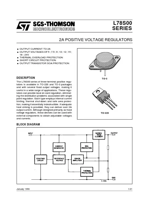
L78S00SERIESJanuary 19932A POSITIVE VOLTAGE REGULATORS.OUTPUT CURRENT TO 2A.OUTPUT VOLTAGES OF 5;7.5;9;10;12;15;18;24V.THERMAL OVERLOAD PROTECTION .SHORT CIRCUIT PROTECTION.OUTPUT TRANSISTOR SOA PROTECTIONDESCRIPTIONThe L78S00series of three-terminal positive regu-lators is available in TO-220and TO-3packages and with several fixed output voltages,making it useful in a wide range of applications.These regu-lators can provide local on-card regulation,eliminat-ing the distribution problems associated with single point regulation.Each type employs internal current limiting,thermal shut-down and safe area protec-tion,making it essentially indestructible.If adequate heat sinking is provided,they can deliver over 2A output current.Although designed primarily as fixed voltage regulators,these devices can be used with external components to obtain adjustable voltages and currents.TO-220BLOCK DIAGRAMTO-31/21ABSOLUTE MAXIMUM RATINGSSymbol Parameter Value UnitV i DC Input Voltage(for V o=5to18V)(for V o=24V)3540VVI o Output Current Internally limitedP t o t Power Dissipation Internally limitedT s t g Storage Temperature–65to+150°CT o p Operating Junction Temperature(for L78S00)(for L78S00C)–55to+1500to+150°C°CTHERMAL DATATO-220TO-3R t h j-cas e R t h j-amb Thermal Resistance Junction-caseThermal Resistance Junction-ambientMaxMax350435°C/W°C/WCONNECTION DIAGRAMS AND ORDERING NUMBERS(top views)Type T O-220T O-3Output Voltage L78S05L78S05C L78S75 L78S75C L78S09 L78S09C L78S10 L78S10C L78S12 L78S12C L78S15 L78S15C L78S18 L78S18C L78S24 L78S24C L78S05CVL78S75CVL78S09CVL78S10CVL78S12CVL78S15CVL78S18CVL78S24CVL78S05TL78S05CTL78S75TL78S75CTL78S09TL78S09CTL78S10TL78S10CTL78S12TL78S12CTL78S15TL78S15CTL78S18TL78S18CTL78S24TL78S24CT5V5V7.5V7.5V9V9V10V10V12V12V15V15V18V18V24V24VL78S00SERIES 2/21L78S00SERIES APPLICATION CIRCUITSCHEMATIC DIAGRAM3/21L78S00SERIESTEST CIRCUITSFigure1:DC Parameters.Figure2:Load Regulation. Figure3:Ripple Rejection.4/21ELECTRICAL CHARACTERISTICS FOR L78S05(refer to the test circuits,T j=25o C,V i=10V,I o=500mA unless otherwise specified)Symbol Parameter Test Conditions Min.Typ.Max.Unit V o Output Voltage 4.85 5.2V V o Output Voltage I o=1A V i=7V 4.755 5.25V∆V o Line Regulation V i=7to25VV i=8to25V 10050mVmV∆V o Load Regulation I o=20mA to2A100mVI d Quiescent Current8mA∆I d Quiescent Current Change I o=20mA to1A0.5mA ∆I d Quiescent Current Change I o=20mA V i=7to25V 1.3mA ∆V o∆TOutput Voltage Drift I o=5mA T j=-55to150o C-1.1mV/o Ce N Output Noise Voltage B=10Hz to100KHz40µVSVR Supply Voltage Rejection f=120Hz60dB V i Operating Input Voltage I o≤1.5A8V R o Output Resistance f=1KHz17mΩI sc Short Circuit Current V i=27V500mAI scp Short Circuit Peack Current3AELECTRICAL CHARACTERISTICS FOR L78S75(refer to the test circuits,T j=25o C,V i=12.5V,I o=500mA unless otherwise specified)Symbol Parameter Test Conditions Min.Typ.Max.Unit V o Output Voltage7.157.57.9V V o Output Voltage I o=1A V i=9.5V7.17.57.95V∆V o Line Regulation V i=9.5to25VV i=10.5to20V 12060mVmV∆V o Load Regulation I o=20mA to2A120mVI d Quiescent Current8mA∆I d Quiescent Current Change I o=20mA to1A0.5mA∆I d Quiescent Current Change I o=20mA V i=9.5to25V 1.3mA∆V o∆TOutput Voltage Drift I o=5mA T j=-55to150o C-0.8mV/o C e N Output Noise Voltage B=10Hz to100KHz52µV SVR Supply Voltage Rejection f=120Hz54dBV i Operating Input Voltage I o≤1.5A10.5VR o Output Resistance f=1KHz16mΩI sc Short Circuit Current V i=27V500mAI scp Short Circuit Peack Current3AL78S00SERIES5/21ELECTRICAL CHARACTERISTICS FOR L78S09(refer to the test circuits,T j=25o C,V i=14V,I o=500mA unless otherwise specified)Symbol Parameter Test Conditions Min.Typ.Max.Unit V o Output Voltage8.6599.35V V o Output Voltage I o=1A V i=11V8.699.4V∆V o Line Regulation V i=11to25VV i=11to20V 13065mVmV∆V o Load Regulation I o=20mA to2A130mVI d Quiescent Current8mA∆I d Quiescent Current Change I o=20mA to1A0.5mA ∆I d Quiescent Current Change I o=20mA V i=11to25V 1.3mA ∆V o∆TOutput Voltage Drift I o=5mA T j=-55to150o C-1mV/o Ce N Output Noise Voltage B=10Hz to100KHz60µVSVR Supply Voltage Rejection f=120Hz53dB V i Operating Input Voltage I o≤1.5A12V R o Output Resistance f=1KHz17mΩI sc Short Circuit Current V i=27V500mAI scp Short Circuit Peack Current3AELECTRICAL CHARACTERISTICS FOR L78S10(refer to the test circuits,T j=25o C,V i=15V,I o=500mA unless otherwise specified)Symbol Parameter Test Conditions Min.Typ.Max.Unit V o Output Voltage9.51010.5V V o Output Voltage I o=1A V i=12.5V9.41010.6V∆V o Line Regulation V i=12.5to30VV i=14to22V 200100mVmV∆V o Load Regulation I o=20mA to2A150mVI d Quiescent Current8mA∆I d Quiescent Current Change I o=20mA to1A0.5mA ∆I d Quiescent Current Change I o=20mA V i=12.5to30V1mA ∆V o∆TOutput Voltage Drift I o=5mA T j=-55to150o C-1mV/o Ce N Output Noise Voltage B=10Hz to100KHz65µVSVR Supply Voltage Rejection f=120Hz53dB V i Operating Input Voltage I o≤1.5A13V R o Output Resistance f=1KHz17mΩI sc Short Circuit Current V i=27V500mAI scp Short Circuit Peack Current3AL78S00SERIES6/21ELECTRICAL CHARACTERISTICS FOR L78S12(refer to the test circuits,T j=25o C,V i=19V,I o=500mA unless otherwise specified)Symbol Parameter Test Conditions Min.Typ.Max.Unit V o Output Voltage11.51212.5V V o Output Voltage I o=1A V i=14.5V11.41212.6V∆V o Line Regulation V i=14.5to30VV i=16to22V 240120mVmV∆V o Load Regulation I o=20mA to2A160mVI d Quiescent Current8mA∆I d Quiescent Current Change I o=20mA to1A0.5mA ∆I d Quiescent Current Change I o=20mA V i=14.5to30V1mA ∆V o∆TOutput Voltage Drift I o=5mA T j=-55to150o C-1mV/o Ce N Output Noise Voltage B=10Hz to100KHz75µVSVR Supply Voltage Rejection f=120Hz53dB V i Operating Input Voltage I o≤1.5A15V R o Output Resistance f=1KHz18mΩI sc Short Circuit Current V i=27V500mAI scp Short Circuit Peack Current3AELECTRICAL CHARACTERISTICS FOR L78S15(refer to the test circuits,T j=25o C,V i=23V,I o=500mA unless otherwise specified)Symbol Parameter Test Conditions Min.Typ.Max.Unit V o Output Voltage14.41515.6V V o Output Voltage I o=1A V i=17.5V14.251515.75V∆V o Line Regulation V i=17.5to30VV i=20to26V 300150mVmV∆V o Load Regulation I o=20mA to2A180mVI d Quiescent Current8mA∆I d Quiescent Current Change I o=20mA to1A0.5mA∆I d Quiescent Current Change I o=20mA V i=17.5to30V1mA∆V o∆TOutput Voltage Drift I o=5mA T j=-55to150o C-1mV/o C e N Output Noise Voltage B=10Hz to100KHz90µV SVR Supply Voltage Rejection f=120Hz52dBV i Operating Input Voltage I o≤1.5A18VR o Output Resistance f=1KHz19mΩI sc Short Circuit Current V i=27V500mAI scp Short Circuit Peack Current3AL78S00SERIES7/21ELECTRICAL CHARACTERISTICS FOR L78S18(refer to the test circuits,T j=25o C,V i=26V,I o=500mA unless otherwise specified)Symbol Parameter Test Conditions Min.Typ.Max.Unit V o Output Voltage17.11818.9V V o Output Voltage I o=1A V i=20.5V171819V∆V o Line Regulation V i=20.5to30VV i=22to28V 360180mVmV∆V o Load Regulation I o=20mA to2A200mVI d Quiescent Current8mA∆I d Quiescent Current Change I o=20mA to1A0.5mA ∆I d Quiescent Current Change I o=20mA V i=22to33V1mA ∆V o∆TOutput Voltage Drift I o=5mA T j=-55to150o C-1mV/o Ce N Output Noise Voltage B=10Hz to100KHz110µVSVR Supply Voltage Rejection f=120Hz49dB V i Operating Input Voltage I o≤1.5A21V R o Output Resistance f=1KHz22mΩI sc Short Circuit Current V i=27V500mAI scp Short Circuit Peack Current3AELECTRICAL CHARACTERISTICS FOR L78S24(refer to the test circuits,T j=25o C,V i=33V,I o=500mA unless otherwise specified)Symbol Parameter Test Conditions Min.Typ.Max.Unit V o Output Voltage232425V V o Output Voltage I o=1A V i=27V22.82425.2V∆V o Line Regulation V i=27to38VV i=30to36V 480240mVmV∆V o Load Regulation I o=20mA to2A250mVI d Quiescent Current8mA∆I d Quiescent Current Change I o=20mA to1A0.5mA ∆I d Quiescent Current Change I o=20mA V i=8to25V1mA ∆V o∆TOutput Voltage Drift I o=5mA T j=-55to150o C-1.5mV/o Ce N Output Noise Voltage B=10Hz to100KHz170µVSVR Supply Voltage Rejection f=120Hz48dB V i Operating Input Voltage I o≤1.5A27V R o Output Resistance f=1KHz23mΩI sc Short Circuit Current V i=27V500mAI scp Short Circuit Peack Current3AL78S00SERIES8/21ELECTRICAL CHARACTERISTICS FOR L78S05C(refer to the test circuits,T j=25o C,V i=10V,I o=500mA unless otherwise specified)Symbol Parameter Test Conditions Min.Typ.Max.Unit V o Output Voltage 4.85 5.2V V o Output Voltage I o=1A V i=7V 4.755 5.25V∆V o Line Regulation V i=7to25VV i=8to12V 10050mVmV∆V o Load Regulation I o=20mA to1.5AI o=2A80100mVI d Quiescent Current8mA∆I d Quiescent Current Change I o=20mA to1A0.5mA ∆I d Quiescent Current Change I o=20mA V i=7to25V 1.3mA ∆V o∆TOutput Voltage Drift I o=5mA T j=0to70o C-1.1mV/o Ce N Output Noise Voltage B=10Hz to100KHz40µVSVR Supply Voltage Rejection f=120Hz54dB V i Operating Input Voltage I o≤1.5A8V R o Output Resistance f=1KHz17mΩI sc Short Circuit Current V i=27V500mAI scp Short Circuit Peack Current3AELECTRICAL CHARACTERISTICS FOR L78S75C(refer to the test circuits,T j=25o C,V i=12.5V,I o=500mA unless otherwise specified)Symbol Parameter Test Conditions Min.Typ.Max.Unit V o Output Voltage7.157.57.9V V o Output Voltage I o=1A V i=9.5V7.17.57.95V∆V o Line Regulation V i=9.5to25VV i=10.5to20V 12060mVmV∆V o Load Regulation I o=20mA to1.5AI o=2A100140mVI d Quiescent Current8mA∆I d Quiescent Current Change I o=20mA to1A0.5mA∆I d Quiescent Current Change I o=20mA V i=9.5to25V 1.3mA∆V o∆TOutput Voltage Drift I o=5mA T j=0to70o C-0.8mV/o C e N Output Noise Voltage B=10Hz to100KHz52µV SVR Supply Voltage Rejection f=120Hz48dBV i Operating Input Voltage I o≤1.5A10.5VR o Output Resistance f=1KHz16mΩI sc Short Circuit Current V i=27V500mAI scp Short Circuit Peack Current3AL78S00SERIES9/21ELECTRICAL CHARACTERISTICS FOR L78S09C(refer to the test circuits,T j=25o C,V i=14V,I o=500mA unless otherwise specified)Symbol Parameter Test Conditions Min.Typ.Max.Unit V o Output Voltage8.6599.35V V o Output Voltage I o=1A V i=11V8.699.4V∆V o Line Regulation V i=11to25VV i=11to20V 13065mVmV∆V o Load Regulation I o=20mA to1.5AI o=2A100170mVI d Quiescent Current8mA∆I d Quiescent Current Change I o=20mA to1A0.5mA ∆I d Quiescent Current Change I o=20mA V i=11to25V 1.3mA ∆V o∆TOutput Voltage Drift I o=5mA T j=0to70o C-1mV/o Ce N Output Noise Voltage B=10Hz to100KHz60µVSVR Supply Voltage Rejection f=120Hz47dB V i Operating Input Voltage I o≤1.5A12V R o Output Resistance f=1KHz17mΩI sc Short Circuit Current V i=27V500mAI scp Short Circuit Peack Current3AELECTRICAL CHARACTERISTICS FOR L78S10C(refer to the test circuits,T j=25o C,V i=15V,I o=500mA unless otherwise specified)Symbol Parameter Test Conditions Min.Typ.Max.Unit V o Output Voltage9.51010.5V V o Output Voltage I o=1A V i=12.5V9.41010.6V∆V o Line Regulation V i=12.5to30VV i=14to22V 200100mVmV∆V o Load Regulation I o=20mA to1.5AI o=2A150240mVI d Quiescent Current8mA∆I d Quiescent Current Change I o=20mA to1A0.5mA ∆I d Quiescent Current Change I o=20mA V i=12.5to30V1mA ∆V o∆TOutput Voltage Drift I o=5mA T j=0to70o C-1mV/o Ce N Output Noise Voltage B=10Hz to100KHz65µVSVR Supply Voltage Rejection f=120Hz47dB V i Operating Input Voltage I o≤1.5A13V R o Output Resistance f=1KHz17mΩI sc Short Circuit Current V i=27V500mAI scp Short Circuit Peack Current3AL78S00SERIES10/21ELECTRICAL CHARACTERISTICS FOR L78S12C(refer to the test circuits,T j=25o C,V i=19V,I o=500mA unless otherwise specified)Symbol Parameter Test Conditions Min.Typ.Max.Unit V o Output Voltage11.51212.5V V o Output Voltage I o=1A V i=14.5V11.41212.6V∆V o Line Regulation V i=14.5to30VV i=16to22V 240120mVmV∆V o Load Regulation I o=20mA to1.5AI o=2A150240mVI d Quiescent Current8mA∆I d Quiescent Current Change I o=20mA to1A0.5mA ∆I d Quiescent Current Change I o=20mA V i=14.5to30V1mA ∆V o∆TOutput Voltage Drift I o=5mA T j=0to70o C-1mV/o Ce N Output Noise Voltage B=10Hz to100KHz75µVSVR Supply Voltage Rejection f=120Hz47dB V i Operating Input Voltage I o≤1.5A15V R o Output Resistance f=1KHz18mΩI sc Short Circuit Current V i=27V500mAI scp Short Circuit Peack Current3AELECTRICAL CHARACTERISTICS FOR L78S15C(refer to the test circuits,T j=25o C,V i=23V,I o=500mA unless otherwise specified)Symbol Parameter Test Conditions Min.Typ.Max.Unit V o Output Voltage14.41515.6V V o Output Voltage I o=1A V i=17.5V14.251515.75V∆V o Line Regulation V i=17.5to30VV i=20to26V 300150mVmV∆V o Load Regulation I o=20mA to1.5AI o=2A150300mV I d Quiescent Current8mA ∆I d Quiescent Current Change I o=20mA to1A0.5mA ∆I d Quiescent Current Change I o=20mA V i=17.5to30V1mA ∆V o∆TOutput Voltage Drift I o=5mA T j=0to70o C-1mV/o C e N Output Noise Voltage B=10Hz to100KHz90µV SVR Supply Voltage Rejection f=120Hz46dB V i Operating Input Voltage I o≤1.5A18V R o Output Resistance f=1KHz19mΩI sc Short Circuit Current V i=27V500mA I scp Short Circuit Peack Current3AELECTRICAL CHARACTERISTICS FOR L78S18C(refer to the test circuits,T j=25o C,V i=26V,I o=500mA unless otherwise specified)Symbol Parameter Test Conditions Min.Typ.Max.Unit V o Output Voltage17.11818.9V V o Output Voltage I o=1A V i=20.5V171819V∆V o Line Regulation V i=20.5to30VV i=22to28V 360180mVmV∆V o Load Regulation I o=20mA to1.5AI o=2A200360mVI d Quiescent Current8mA∆I d Quiescent Current Change I o=20mA to1A0.5mA ∆I d Quiescent Current Change I o=20mA V i=20.5to30V1mA ∆V o∆TOutput Voltage Drift I o=5mA T j=0to70o C-1mV/o Ce N Output Noise Voltage B=10Hz to100KHz110µVSVR Supply Voltage Rejection f=120Hz43dB V i Operating Input Voltage I o≤1.5A21V R o Output Resistance f=1KHz22mΩI sc Short Circuit Current V i=27V500mAI scp Short Circuit Peack Current3AELECTRICAL CHARACTERISTICS FOR L78S24C(refer to the test circuits,T j=25o C,V i=33V,I o=500mA unless otherwise specified)Symbol Parameter Test Conditions Min.Typ.Max.Unit V o Output Voltage232425V V o Output Voltage I o=1A V i=27V22.82425.2V∆V o Line Regulation V i=27to38VV i=30to36V 480240mVmV∆V o Load Regulation I o=20mA to1.5AI o=2A300480mV I d Quiescent Current8mA ∆I d Quiescent Current Change I o=20mA to1A0.5mA ∆I d Quiescent Current Change I o=20mA V i=27to38V1mA ∆V o∆TOutput Voltage Drift I o=5mA T j=0to70o C-1.5mV/o C e N Output Noise Voltage B=10Hz to100KHz170µV SVR Supply Voltage Rejection f=120Hz42dB V i Operating Input Voltage I o≤1.5A27V R o Output Resistance f=1KHz28mΩI sc Short Circuit Current V i=27V500mA I scp Short Circuit Peack Current3AFigure6:Supply Voltage Rejection vs.Frequen-cy.Figure7:Output Voltage vs.Junction Tempera-ture.Figure4:Dropout Voltage vs.Junction Tempera-ture.Figure5:Peak Output Current vs.Input/Output Differential Voltage.Figure8:Output Impedance vs.Frequency.Figure9:Quiescent Current vs.Junction Tempe-rature.Figure12:Quiescent Current vs.Input Voltage.Figure13:Fixed Output Regulator.Figure14:Constant Current Regulator. Figure10:Load Transient Response.Figure11:Line Transient Response.Notes:1.To specify an output voltage,substitute voltage value for”XX”.2.Although no output capacitor is needed for sta-bility,it does improve transient response.3.Required if regulator is located an appreciabledis-tance from power supply filter.V XXI O=+I dR1Figure 15:Circuit for Increasing Output Voltage.Figure 16:Adjustable Output Regulator(7to 30V).Figure 17:0.5to 10V Regulator.Figure 18:High Current Voltage Regulator.V BEQ 1R 1=I Q 1I REQ –βQ 1V BEQ 1I O =I REG +Q 1[I REG –]R 1R 4V O =V XXR 1I R1≥5I d R 2V 0=V XX (1+)+I d R 2R 1Figure 19:High Output Current with Short CircuitProtection.Figure 20:Tracking Voltage Regulator.V BEQ 2R SC =I SCFigure21:Positive and Negative Regulator.Figure22:Negative Output Voltage Circuit. (*)D1and D2are necessary if the load is connected be-tween+V0and–V0.Figure23:Switching Regulator.Figure24:High Input Voltage Circuit.V IN=V i–(V Z+V BE)Figure25:High Input Voltage Circuit.Figure26:High Output VoltageRegulator. V IN=V Z-V BEFigure 27:High Input and Output Voltage.Figure 28:Reducing Power Dissipation withDropping Resistor.V O =V XX +V Z1V i(min)–V XX –V DROP(max)R =I O(max)+I d(max)Figure 29:Remote Shuntdown.Figure 30:Power AM Modulator (unity voltagegain,Io ≤1A).Note :The circuit performs well up to 100KHz.Figure 31:Adjustable Output Voltage with Tem-perature Compensation.Note :Q 2is connected as a diode in order to compensatethe variati on of the Q 1V BE with the temperature.C allows a slow rise-time of the V OR 2V O =V XX (1+)+V BE R 1Figure32:Light Controllers(V o min=V xx+V BE).V O falls when the light goes up V O rises when the light goes up Figure33:Protection against Input Short-circuitwith High Capacitance Loads.Applications with high capacitance loads and anoutput voltage greater than6volts need an externaldiode(see fig.33)to protect the device against inputshort circuit.In this case the input voltage fallsrapidly while the output voltage decreases showly.The capacitance discharges by means of the Base-Emitter junction of the series pass transistor in theregulator.If the energy is sufficiently high,the tran-sistor may be destroyed.The external diode by-passes the current from the IC to ground.DIM.mm inchMIN.TYP.MAX.MIN.TYP.MAX. A11.0013.100.4330.516 B0.97 1.150.0380.045 C 1.50 1.650.0590.065 D8.328.920.3270.351 E19.0020.000.7480.787 G10.7011.100.4210.437 N16.5017.200.6490.677 P25.0026.000.984 1.023 R 4.00 4.090.1570.161 U38.5039.30 1.515 1.547 V30.0030.30 1.187 1.193CDN BVUR APEGOP003F TO-3MECHANICAL DATADIM.mminch MIN.TYP.MAX.MIN.TYP.MAX.A 4.40 4.600.1730.181C 1.23 1.320.0480.051D 2.402.720.0940.107D1 1.270.050E 0.490.700.0190.027F 0.610.880.0240.034F1 1.14 1.700.0440.067F2 1.14 1.700.0440.067G 4.95 5.150.1940.203G1 2.4 2.70.0940.106H210.010.400.3930.409L216.40.645L413.014.00.5110.551L5 2.65 2.950.1040.116L615.215.90.5980.625L7 6.2 6.60.2440.260L9 3.5 4.20.1370.165DIA.3.75 3.850.1470.151L6ACDED 1FGL7L2Dia.F 1L5L4H 2L9F 2G 1TO-220MECHANICAL DATAP011C元器件交易网L78S00SERIES Information furnished is believed to be accurate and reliable.However,SGS-THOMSON Microelectronics assumes no responsability for theconsequences of use of such information nor for any infringement of patents or other rights of third parties which may results from its use.Nolicense is granted by implication or otherwise under any patent or patent rights of SGS-THOMSON Microelectronics.Specificationsmentionedin this publication are subject to change without notice.This publication supersedes and replaces all information previously supplied.SGS-THOMSON Microelectronics products are not authorized for use ascritical components in life support devices or systems without expresswritten approval of SGS-THOMSON Microelectonics.©1994SGS-THOMSON Microelectronics-All Rights ReservedSGS-THOMSON Microelectronics GROUP OF COMPANIESAustralia-Brazil-France-Germany-Hong Kong-Italy-Japan-Korea-Malaysia-Malta-Morocco-The Netherlands-Singapore-Spain-Sweden-Switzerland-Taiwan-Thailand-United Kingdom-U.S.A21/21。
2SK1358中文资料

MIN.
– – 900 1.5 – 2.0 – – – – – – –
TYP.
– – – – 1.1 4.0 1300 100 180 25 40 20 100
MAX.
±100 300 0 50 80 40 200
UNIT
nA µA V V Ω S pF
2sk1358 toshibatoshiba corporation 1/6 discrete semiconductors 2sk1358 field effect transistor silicon channelmos type -mosii.5) high speed, high current dc-dc converter, relay drive motordrive applications features lowdrain-source highforward transfer admittance 4.0s(typ.) lowleakage current electrostaticsensitive device. please handle care.absolute maximum ratings (ta characteristicsymbol rating unit drain-source voltage dss900 drain-gatevoltage dgr900 gate-sourcevoltage draincurrent dc dp27 drain power dissipation (tc channeltemperature ch150 storagetemperature range stg-55 thermalcharacteristics characteristic symbol max. unit thermal resistance, channel th(ch-c)0.833 thermalresistance, channel th(ch-a)50 mmindustrial applications 2/6 toshiba corporation 2sk1358 source-drain diode ratings characteristics(ta electricalcharacteristics (ta characteristicsymbol test condition min. typ. max. unit gate leakage current 100na drain cut-off current drain-sourcebreakdown voltage (br)dss 0v900 gatethreshold voltage
HCS08系列微控制器参考手册(中文)

HCS08系列微控制器参考手册第一册苏州大学飞思卡尔嵌入式系统研发中心翻译 2009年11月目录第一章通用信息与结构框图 (1)1.1HCS08系列微控制器介绍 (1)1.2HCS08CPU编程模型 (2)1.3外设模块 (2)1.4MC9S08GB60的特点 (3)1.4.1 HCS08系列的共性 (3)1.4.2 MC9S08GB60的特点 (3)1.5MC9S08GB60的结构框图 (4)第二章引脚及其连接 (5)2.1简介 (5)2.2推荐的系统连接 (5)2.2.1 电源 (7)2.2.2 MC9S08GB60振荡器 (7)2.2.3 复位 (8)2.2.4 背景/模式选择(BKGD/MS) (8)2.2.5 通用I/O及外设端口 (8)第三章工作模式 (10)3.1简介 (10)3.2特征 (10)3.3运行模式 (10)3.4背景调试模式 (11)3.5等待模式 (12)3.6停止模式 (12)3.6.1 Stop1模式 (13)3.6.2 Stop2模式 (13)3.6.3 Stop3模式 (14)3.6.4 停止模式下激活BDM使能 (14)3.6.5 设置OSCSTEN位 (15)3.6.6 停止模式下LVD使能 (15)3.6.7 停止模式下的片上外设模块 (15)3.6.8 系统选择寄存器(SOPT) (17)3.6.9 系统电源管理状态和控制寄存器1(SPMSC1) (18)3.6.10 系统电源管理状态和控制寄存器2(SPMSC2) (19)第四章片上存储器 (21)4.1简介 (21)4.2HCS08核定义的存储器组织 (21)4.2.1 HCS08存储器组织 (21)4.2.2 MC9S08GB60存储映像 (22)4.2.3 复位和中断向量表 (23)4.3寄存器地址和位分配 (24)4.4RAM (29)4.560K字节的FLASH (29)4.5.1 特征 (30)4.5.2 写入、擦除和空白检测命令 (30)4.5.3 命令时间和突发模式写入 (32)4.5.3.1 行和FLASH的组织结构 (32)4.5.3.2 程序命令时序 (33)4.5.4 访问错误 (34)4.5.5 向量重定向 (34)4.5.6 FLASH块保护(MC9S08GB60) (34)4.6MC9S08GB60的安全性 (35)4.7MC9S08GB60的FLASH寄存器和控制位 (36)4.7.1 FLASH时钟分频寄存器(FCDIV) (36)4.7.2 FLASH选项寄存器(FOPT和NVOPT) (37)4.7.3 FLASH配置寄存器(FCNFG) (38)4.7.4 FLASH保护寄存器(FPROT和NVPROT) (38)4.7.5 FLASH状态寄存器(FSTAT) (39)4.7.6 FLASH命令寄存器(FCMD) (40)4.8FLASH存储器应用实例 (41)4.8.1 FLASH模块时钟的初始化 (41)4.8.2 擦除FLASH的一页(512字节) (42)4.8.3 DoOnStack子程序 (43)4.8.4 SpSub子程序 (45)4.8.5 FLASH的字节编程 (46)第五章复位和中断 (47)5.1简介 (47)5.2MC9S08GB60复位和中断的特征 (47)5.4计算机正常操作监控模块(COP)看门狗 (48)5.5中断 (48)5.5.1 中断堆栈结构 (49)5.5.2 外部中断请求(IRQ)引脚 (50)5.5.2.1 引脚配置选项 (50)5.5.2.2 边沿/电平触发 (50)5.5.3 中断向量、中断源和局部屏蔽 (51)5.6低电压检测系统(LVD) (52)5.6.1 上电复位操作 (52)5.6.2 LVD复位操作 (52)5.6.3 LVD中断操作 (53)5.6.4 低电压警告(LVW) (53)5.7实时中断(RTI) (53)5.8复位、中断以及系统控制寄存器和控制位 (53)5.8.1 中断请求状态和控制寄存器(IRQSC) (54)5.8.2 系统复位状态寄存器(SRS) (55)5.8.3 系统背景调试强制复位寄存器(SBDFR) (56)5.8.4 系统选项寄存器(SOPT) (56)5.8.5 系统设备识别寄存器(SDIDH、SDIDL) (57)5.8.6 系统实时中断状态和控制寄存器(SRTISC) (57)5.8.7 系统电源管理状态控制寄存器1(SPMSC1) (58)5.8.8 系统电源管理状态和控制寄存器2(SPMSC2) (59)第六章中央处理单元 (61)6.1简介 (61)6.2编程结构和CPU寄存器 (61)6.2.1 累加器(A) (62)6.2.2 变址寄存器(H:X) (63)6.2.3 堆栈指针(SP) (64)6.2.4 程序计数器(PC) (66)6.2.5 条件码寄存器(CCR) (66)6.3寻址方式 (70)6.3.1 隐含寻址方式(INH) (71)6.3.2 相对寻址方式(REL) (71)6.3.3 立即寻址方式(IMM) (72)6.3.4 直接寻址方式(DIR) (72)6.3.5 扩展寻址方式(EXT) (72)6.3.6.1 无偏移量变址方式(IX) (73)6.3.6.2 无偏移量变址、变址加1寻址方式(IX+) (73)6.3.6.3 8位偏移量变址方式(IX1) (73)6.3.6.4 8位偏移量变址、变址加1寻址方式(IX1+) (73)6.3.6.5 16位偏移量变址方式(IX2) (73)6.3.6.6 8位偏移量堆栈寻址方式(SP1) (74)6.3.6.7 16位偏移量堆栈寻址方式(SP2) (74)6.4特殊操作 (75)6.4.1 复位序列 (75)6.4.2 中断 (76)6.4.3 等待模式 (76)6.4.4 停止模式 (76)6.4.5 背景模式 (77)6.4.6 总线周期的用户观点 (77)6.5通过指令类别进行指令集描述 (78)6.5.1 数据传送指令 (78)6.5.1.1 加载与存储 (78)6.5.1.2 位的置位与清零 (81)6.5.1.3 存储器到存储器的传送 (82)6.5.1.4 寄存器传输和半字节交换 (82)6.5.2 算术运算指令 (83)6.5.2.1 加、减、乘和除指令 (83)6.5.2.2 加一、减一、清零和求补 (88)6.5.2.3 比较和测试 (88)6.5.2.4 BCD的计算 (88)6.5.3 逻辑操作指令 (89)6.5.3.1 与、或、异或与求补 (90)6.5.3.2 位测试指令 (91)6.5.4 移位类指令 (91)6.5.5 跳转、转移和循环控制指令 (93)6.5.5.1 无条件跳转和转移指令 (94)6.5.5.2 简单转移 (95)6.5.5.3 有符号转移 (95)6.5.5.4 无符号转移 (95)6.5.5.5 位条件转移 (96)6.5.5.6 循环控制 (96)6.5.6 相关堆栈指令 (97)6.6指令简表 (102)6.7汇编语言指南 (114)6.7.1 列表行 (115)6.7.2 汇编指令 (116)6.7.2.1 BASE——设定编译器的缺省数进制 (116)6.7.2.2 INCLUDE——指定附加源文件 (116)6.7.2.3 NOLIST/LIST——关闭或打开程序列表 (116)6.7.2.4 ORG——设置程序的起始位置 (117)6.7.2.5 EQU——把一个标号和一个数值相关联 (118)6.7.2.6 dc.b——定义存储器中字节化常量 (119)6.7.2.7 dc.w——在存储器中定义16位(字)常量 (119)6.7.2.8 ds.b——定义存储(保留)内存变量字节 (120)6.7.3 标号 (121)6.7.4 表达式 (122)6.7.5 通用文件协议 (123)6.7.6 目标代码(S19)文件 (125)第七章开发支持 (129)7.1介绍 (129)7.2特点 (130)7.3背景调试控制器(BDC) (130)7.3.1 BKGD引脚描述 (131)7.3.2 通信细节 (132)7.3.2.1 BDC通信速率考虑事项 (132)7.3.2.2 位时序细节 (133)7.3.3 BDC寄存器和控制位 (135)7.3.3.1 BDC状态和控制寄存器 (135)7.3.3.2 BDC断点匹配寄存器 (137)7.3.4 BDC命令 (137)7.3.4.1 SYNC——要求时序参考脉冲 (138)7.3.4.2 ACK_ENABLE (139)7.3.4.3 ACK_DISABLE (139)7.3.4.4 BACKGROUND (139)7.3.4.5 READ_STATUS (140)7.3.4.6 WRITE_CONTROL (140)7.3.4.7 READ_BYTE (141)7.3.4.8 READ_BYTE_WS (142)7.3.4.10 WRITE_BYTE (143)7.3.4.11 WRITE_BYTE_WS (143)7.3.4.12 READ_BKPT (144)7.3.4.13 WRITE_BKPT (144)7.3.4.14 GO (144)7.3.4.15 TRACE1 (145)7.3.4.16 TAGGO (145)7.3.4.17 READ_A (145)7.3.4.18 READ_CCR (145)7.3.4.19 READ_PC (146)7.3.4.20 READ_HX (146)7.3.4.21 READ_SP (147)7.3.4.22 READ_NEXT (147)7.3.4.23 READ_NEXT_WS (148)7.3.4.24 WRITE_A (148)7.3.4.25 WRITE_CCR (148)7.3.4.26 WRITE_PC (149)7.3.4.27 WRITE_HX (149)7.3.4.28 WRITE_SP (149)7.3.4.29 WRITE_NEXT (149)7.3.4.30 WRITE_ NEXT_WS (150)7.3.5 串行接口硬件握手协议 (150)7.3.6 取消握手协议 (152)7.3.7 BDC硬件断点 (155)7.3.8 与M68HC12BDM的不同之处 (155)7.3.8.1 8位体系结构 (156)7.3.8.2 命令格式 (156)7.3.8.3 状态位的读写 (156)7.3.8.4 BDM与停止和等待模式 (157)7.3.8.5 SYNC指令 (157)7.3.8.6 硬件断点 (157)7.4标识部分和BDC强制复位 (158)7.4.1 系统设备识别寄存器(SDIDH:SDIDL) (158)7.4.2 系统背景调试强制复位寄存器 (158)7.5片上调试系统(DBG) (159)7.5.1 比较器A和B (159)7.5.2总线信息捕捉和FIFO操作 (160)7.5.4 标记与强制断点和触发器 (161)7.5.5 CPU断点请求 (162)7.5.6 触发模式 (162)7.5.6.1 单独A触发模式 (163)7.5.6.2 A或B触发模式 (163)7.5.6.3 A然后B触发模式 (163)7.5.6.4 事件B触发模式(存储数据) (163)7.5.6.5 A然后事件B触发模式(存储数据) (163)7.5.6.6 A和B数据触发(全模式) (164)7.5.6.7 A与非B数据触发(全模式) (164)7.5.6.8 触发范围内:A≤地址≤B (164)7.5.6.9 触发范围外:地址<A 或者地址>B (164)7.5.7 DBG寄存器和控制位 (165)7.5.7.1 调试比较器A的高地址页寄存器(DBGCAH) (165)7.5.7.2 调试比较器A的低位寄存器(DBGCAL) (165)7.5.7.3 调试比较器B的高地址页寄存器(DBGCAH) (165)7.5.7.4 调试比较器B的低位寄存器(DBGCAL) (165)7.5.7.5 调试FIFO高地址页寄存器(DBGFH) (165)7.5.7.6 调试FIFO低位寄存器(DBGFL) (165)7.5.7.7 调试控制寄存器(DBGC) (166)7.5.7.8 调试触发寄存器(DBGT) (167)7.5.7.9 调试状态寄存器(DBGS) (168)7.5.8 应用信息与举例 (169)7.5.8.1 定向的调试器例子 (171)7.5.8.2 例1:终止对地址A的处理 (171)7.5.8.3 例2:终止对地址A指令的处理 (172)7.5.8.4 例3:终止在地址A或B上的指令处理 (172)7.5.8.5 例4:开始跟踪在地址A的指令 (173)7.5.8.6 例5:A到B顺序后停止的尾部跟踪 (173)7.5.8.7 例6:起始跟踪数据B写入地址A (174)7.5.8.8 例7:从地址B中读取被捕获的首八位数据 (174)7.5.8.9 例8:捕获在读地址A后写入到地址B的值 (175)7.5.8.10 例9:在一个例程中触发所有的执行命令 (175)7.5.8.11 例10:通过触发来试图处理外部FLASH (176)7.5.9 硬件断点和ROM修补 (176)附录A 指令集详述 (177)A.2命名规则 (177)A.3规范定义 (180)A.4指令集 (180)ADC Add with Carry(带进位位加) (180)ADD Add without Carry(无进位位加) (181)AIS Add Immediate Value to Stack Pointer(立即数加到SP) (182)AIX Add Immediate Value to Index Register(立即数加到HX) (182)AND Logical AND(逻辑与) (183)ASL Arithmetic Shift Left(算术左移) (184)ASR Arithmetic Shift Right(算术右移) (184)BCC Branch if Carry Bit Clear(C为0则转移) (185)BCLR n Clear Bit n in Memory(内存单元n位清零) (185)BCS Branch if Carry Bit Set(C为1则转移) (186)BEQ Branch if Equal(等于则转移) (187)BGE Branch if Greater Than or Equal To(大于或等于则转移) (187)BGND Background(进入背景调试模式) (188)BGT Branch if Greater Than(大于则转移) (188)BHCC Branch if Half Carry Bit Clear(H为0则转移) (189)BHCS Branch if Half Carry Bit Set(H为1则转移) (189)BHI Branch if Higher(大于则转移) (190)BHS Branch if Higher or Same(大于或等于则转移) (191)BIH Branch if IRQ Pin High(引脚IRQ为1则转移) (191)BIL Branch if IRQ Pin Low(引脚IRQ为0则转移) (192)BIT Bit Test(位测试) (192)BLE Branch if Less Than or Equal To(小于或等于则转移) (193)BLO Branch if Lower(小于则转移) (193)BLS Branch if Lower or Same(小于或等于则转移) (194)BLT Branch if Less Than(小于则转移) (195)BMC Branch if Interrupt Mask Clear(I为0则转移) (195)BMI Branch if Minus(结果为负则转移) (196)BMS Branch if Interrupt Mask Set(I为1则转移) (196)BNE Branch if Not Equal(不等于则转移) (197)BPL Branch if Plus(结果为正则转移) (197)BRA Branch Always(无条件短转移) (198)BRCLR n Branch if Bit n in Memory Clear(M位n为0则转移) (199)BRN Branch Never(三个总线周期的空操作) (200)BRSET n Branch if Bit n in Memory Set(M位n为1则转移) (200)BSET n Set Bit n in Memory(M位n置1) (201)BSR Branch to Subroutine(转移到子程序) (201)CBEQ Compare and Branch if Equal(比较,等于则转移) (202)CLC Clear Carry Bit(进位位C清零) (203)CLI Clear Interrupt Mask Bit(中断屏蔽位I清零) (203)CLR Clear(清零) (204)CMP Compare Accumulator with Memory(A与M比较) (204)COM Complement(按位取反) (205)CPHX Compare Index Register with Memory(HX与M比较) (206)CPX Compare X with Memory(X与M比较) (207)DAA Decimal Adjust Accumulator(A十进制调整) (208)DBNZ Decrement and Branch if Not Zero(减1不为0则转移) (209)DEC Decrement(自减1) (209)DIV Divide(无符号除法) (210)EOR Exclusive-OR Memory with Accumulator(M与A异或) (211)INC Increment(自加1) (211)JMP Jump(无条件跳转) (212)JSR Jump to Subroutine(跳转到子程序) (213)LDA Load Accumulator form Memory(取M内容到A) (213)LDHX Load Index Register form Memory(取M内容到HX) (214)LDX Load X from Memory(取M内容到X) (215)LSL Logical Shift Left(逻辑左移) (215)LSR Logical Shift Right(逻辑右移) (216)MOV Move(M单元间数据传送) (217)MUL Unsigned Multiply(无符号数乘法) (218)NEG Negate(Two’s Complement) (求补) (218)NOP No Operation(空操作) (219)NSA Nibble Swap Accumulator(A的高低4位对调) (219)ORA Inclusive-OR Accumulator and Memory(逻辑或) (220)PSHA Push Accumulator onto Stack(A进栈) (220)PSHH Push H onto Stack(H进栈) (221)PSHX Push X onto Stack(X进栈) (221)PULA Pull Accumulator from Stack(A出栈) (222)PULH Pull H from Stack(H出栈) (222)PULX Pull X from Stack(X出栈) (223)ROL Rotate Left through Carry(带进位位的循环左移) (223)ROR Rotate Right through Carry(带进位位的循环右移) (224)RSP Reset Stack Pointer(堆栈指针置$FF) (224)RTI Return from interrupt(中断返回) (225)RTS Return from Subroutine(子程序返回) (226)SBC Subtract with Carry(带借位减法) (226)SEC Set Carry Bit(进位位置位) (227)SEI Set Interrupt Mask Bit(中断屏蔽位置位) (227)STA Store Accumulator in Memory(A存入M) (228)STHX Store Index Register(HX存入M) (229)STOP Enable IRQ Pin, Stop Processing(停机) (229)STX Store X in Memory(X存入M) (230)SUB Subtract(无借位减法) (231)SWI Software Interrupt(软件中断) (231)TAP Transfer Accumulator to Processor Status Byte(写CCR) (232)TAX Transfer Accumulator to X(A复制到X) (233)TPA Transfer Processor Status Byte to Accumulator(读CCR) (233)TST Test for Negative or Zero(小于或等于0测试) (234)TSX Transfer Stack Pointer to index Register(复制SP到HX) (235)TXA Transfer X to Accumulator(复制X到A) (235)TXS Transfer Index Register Low to Stack Pointer(HX-1写入SP) (235)WAIT Enable Interrupts; Stop Processor(待机) (236)附录B 通用文件规范 (237)B.1引言 (237)B.2存储映射区域划分 (238)B.3中断向量定义 (238)B.4位定义的两种方式 (239)B.5MC9S08GB60完整的通用文件 (240)第一章通用信息与结构框图1.1 HCS08系列微控制器介绍新型的FreescaleHCS08系列微控制器,尽管包含新指令,可以执行快速调试和开发功能,但仍然和旧的M68HC08系列完全兼容。
LT1357CS8中文资料
Consult factory for Industrial and Military grade parts.
ELECTRICAL CHARACTERISTICS
SYMBOL VOS PARAMETER Input Offset Voltage CONDITIONS
TA = 25°C, VCM = 0V unless otherwise noted.
元器件交易网
LT1357 25MHz, 600V/µs Op Amp
FEATURES
s s s s s s s s s s s s s s s
DESCRIPTION
The LT ®1357 is a high speed, very high slew rate operational amplifier with outstanding AC and DC performance. The LT1357 has much lower supply current, lower input offset voltage, lower input bias current, and higher DC gain than devices with comparable bandwidth. The circuit topology is a voltage feedback amplifier with the slewing characteristics of a current feedback amplifier. The amplifier is a single gain stage with outstanding settling characteristics which makes the circuit an ideal choice for data acquisition systems. The output drives a 500Ω load to ±12V with ±15V supplies and a 150Ω load to ± 2.5V on ±5V supplies. The amplifier is also stable with any capacitive load which makes it useful in buffer or cable driver applications. The LT1357 is a member of a family of fast, high performance amplifiers using this unique topology and employing Linear Technology Corporation’s advanced bipolar complementary processing. For dual and quad amplifier versions of the LT1357 see the LT1358/LT1359 data sheet. For higher bandwidth devices with higher supply current see the LT1360 through LT1365 data sheets. For lower supply current amplifiers see the LT1354 and LT1355/ LT1356 data sheets. Singles, duals, and quads of each amplifier are available.
CS1258系列AFE用户手册v02
CS1258 芯片用户手册带24bits ADC 和BIM 的高性能AFEREV0.2 通讯地址:深圳市南山区蛇口南海大道1079 号花园城数码大厦A座9楼邮政编码:518067公司电话:+(86 755)86169257传真:+(86 755)86169057公司网站:CS1258 芯片用户手册版本历史修改记录日期0.1 预览版本2016/3/15 0.2 .更新了电气特性2016/3/29.更新了典型应用图.更新了封装图目录版本历史 (2)目录 (3)图目录 (5)表目录 (5)1 简介 (6)1.1 主要特性 (6)1.2 应用场合 (6)1.3 功能说明 (6)1.4 极限值 (8)1.5 电气特性 (9)1.6 可靠性指标 (10)1.7 产品型号及引脚 (11)1.8 典型应用电路 (12)2 功能寄存器说明 (13)2.1 功能寄存器列表 (13)2.2 功能寄存器说明 (13)2.2.1 SYS —系统配置寄存器 (13)2.2.2 ADC0— ADC 配置寄存器 (14)2.2.3 ADC1— ADC 配置寄存器1 (14)2.2.4 ADC2— ADC 配置寄存器2 (15)2.2.5 ADC3— ADC 配置寄存器3 (15)2.2.6 ADC4— ADC 配置寄存器4 (16)2.2.7 ADC5— ADC 配置寄存器5 (16)2.2.8 BIM0— BIM 配置寄存器0 (17)2.2.9 BIM1— BIM 配置寄存器 (17)2.2.10 ADO— ADC 转换数据寄存器 (18)2.2.11 ADS— ADC 转换数据读取标准寄存器 (18)3 功能描述 (19)3.1 输入选择 (19)3.2 输入电平移位器 (19)3.3 IDAC1/IDAC0 和输入通道 (20)3.4 PGA 和ADC (21)3.5 数字滤波器 (23)3.5.1 频率响应 (23)3.5.2 建立时间 (23)3.6 人体阻抗测量 (25)3.6.1 正弦信号发生器 (25)3.6.2 激励电极及测量电极 (26)3.6.3 整流 (26)3.6.4 阻抗校准 (27)3.7 参考电压源 (28)3.8 内部时钟源 (28)3.9 温度传感器 (28)3.10 测量模式及其切换 (28)3.11 多种工作模式 (29)3.12 复位和断电(POR&power down) (30)4 转换有效位 (31)5 典型特性 (32)5.1 ADC 典型特性 (32)5.2 LDO/VREF 典型特性 (32)5.3 内部时钟典型特性 (32)5.4 IDAC 典型特性 (32)5.5 BIM 典型特性 (32)6 三线串行通讯接口 (37)6.1.1 读时序 (38)6.1.2 写时序 (38)7 封装 (40)图目录图 1.1 CS1258 原理框图 (7)图 1.2 CS1258 引脚图 (11)图 1.3 CS1258 典型应用电路 (12)图 3.1 模拟输入结构图 (19)图 3.2 电平移位模块 (20)图 3.3 IDAC1/IDAC0 结构及与输入通道关系 (20)图 3.4 PGA 和ADC 结构图 (21)图 3.5 COMB 滤波器的频率响应特性(Fs=331Hz,DR=10Hz,3 阶COMB) (23)图 3.6 COMB 建立过程 (24)图 3.7 BIM 模块结构图 (25)图 3.8 CS1258 低功耗工作示意图 (29)图 5.1 内部时钟全电压全温度范围的典型特性 (32)图 5.2 FWR 模式下220 欧姆纯电阻网络的测试结果 (33)图 5.3 FWR 模式下1000 欧姆纯电阻网络的测试结果 (33)图 5.4 FWR 模式下1958 欧姆纯电阻网络的测试结果 (34)图 5.5 FWR+MIX 模式510ohm+470pF 并联网络的阻抗绝对值测试结果 (34)图 5.6 FWR+MIX 模式510ohm+470pF 并联网络的相位角测试结果 (35)图 5.7 FWR+MIX 模式1018Ohm+10nF 并联网络的阻抗绝对值测试结果 (35)图 5.8 FWR+MIX 模式1018Ohm+10nF 并联网络的相位角测试结果 (36)图 6.1 读操作时序1(读AD 值) (38)图 6.2 读操作时序2(除AD 值之外的寄存器) (38)图 6.3 写操作时序 (39)图7.1 芯片LQFP32 封装尺寸信息(天水) (40)表目录表 1.1 CS1258 极限值 (8)表 1.2 CS1258 电气特性 (9)表 1.3 CS1258 引脚说明 (11)表 2.1 功能寄存器列表 (13)表 2.2 SYS 寄存器说明 (13)表 2.3 ADC0 寄存器说明 (14)表 2.4 ADC1 寄存器说明 (14)表 2.5 ADC2 寄存器说明 (15)表 2.6 ADC3 寄存器说明 (15)表 2.7 ADC4 寄存器说明 (16)表 2.8 ADC5 寄存器说明 (16)表 2.9 BIM0 寄存器说明 (17)表 2.10 BIM1 寄存器说明 (17)表 4.1 ADC 信号链不同GAIN 及DR 下的有效位(ENOB)1) (31)表 6.1 串口通讯命令列表 (37)表 6.2 三线串行通讯接口时序表 (39)版权所有,侵权必究芯海科技(深圳)股份有限公司第 5 页,共40 页1 简介1.1 主要特性◆输入●支持单端输入●支持组成多个差分输入对●支持输入电平移位功能◆PGA●1/2/4/8/16/32/64/128 倍可选增益●高达100Mohm 的等效输入阻抗◆BIM●支持4/6/8 电极测量●支持5K/10K/25K/50K/100K/250KHz 多档频率测量●支持阻抗绝对值和相角测量◆ADC●24 bit 分辨率●输出速率10~1280Hz 8 档可选◆有效位● 2.35V 参考、40Hz 速率、128 倍增益下19.5bits 有效位◆LDO 及内部参考电压●自带LDO,输出2.35/2.45/2.8/3.0V 可选,精度±1%●自带低漂移基准,内部参考电压2.048V 可选,精度±1%◆支持性能、普通、低功耗、休眠模式◆支持电压测量、温度测量、BIM 测量及手动测量模式,单命令切换◆低漂移片上时钟◆三线串行通讯1.2 应用场合桥式传感器四角平衡称重压力检测人体阻抗分析交流测脂1.3 功能说明CS1258 原理框图如图1 所示。
LT3580中文资料
SYNC Voltage............................................ –0.3V to 5.5V Operating Junction Temperature Range
LT3580E (Notes 2, 5) .........................–40°C to 125°C LT3580I (Notes 2, 5)..........................–40°C to 125°C Storage Temperature Range...................–65°C to 150°C
2
2.2
200 220
1/4
2500
mA μA %/V MHz kHz Ratio kHz
SYNC High Level for Synchronization
l 1.3
V
SYNC Low Level for Synchronization
VSHDN = 2.5V, Not Switching VSHDN = 0V 2.5V ≤ VIN ≤ 32V RT = 45.3k RT = 464k Compared to Normal fOSC SYNCing or Free Running
l 1.8 l 180
l 200
1
1.5
0
1
0.01 0.05
元器件交易网
LT3580
Boost/Inverting DC/DC Converter with 2A Switch, Soft-Start, and Synchronization
FEATURES
n 2A Internal Power Switch n Adjustable Switching Frequency n Single Feedback Resistor Sets VOUT n Synchronizable to External Clock n High Gain SHDN Pin Accepts Slowly Varying
LT1057ACN8中文资料
NUMBER
LT1057S8 LT1057IS8
+
C 12 +IN C
S8 PACKAGE
S8 PART MARKING
–
11 –IN C 10 OUT C
8-LEAD PLASTIC SO TJMAX = 150°C, θJA = 200°C/W
1057
9 NC
Please note that the LT1057S8/LT1057IS8 standard surface mount pinout differs from that of the LT1057 standard CERDIP/PDIP packages.
Both the LT1057 and LT1058 are available in the plastic PDIP package and the surface mount SO package.
, LT, LTC and LTM are registered trademarks of Linear Technology Corporation. All other trademarks are the property of their respective owners.
DESCRIPTION
The LT®1057 is a matched JFET input dual op amp in the industry standard 8-pin configuration, featuring a combination of outstanding high speed and precision specifications. It replaces all the popular bipolar and JFET input dual op amps. In particular, the LT1057 upgrades the performance of systems using the LF412A and OP-215 JFET input duals.