Bifacial Solar Cells Based on Isotype Junctions
重新定义护肤科技

重新定义护肤科技
王敏
【期刊名称】《科技资讯》
【年(卷),期】2004(000)005
【摘要】著名护肤品牌OLAY再次挑战传统护肤理念,首次向中国媒体介绍领先国际护肤领域的生物科技成分Amino-peptide(氨基酸肽),从而使护肤产品突破到细胞护理的层面。
【总页数】2页(P17-18)
【作者】王敏
【作者单位】
【正文语种】中文
【中图分类】TS974.2
【相关文献】
1.直击联想科技创新大会:“黑科技”重新定义联想 [J], 刘启诚
2.欧华引入国际尖端科技增强其护肤品科技含量 [J], 无
3.重新定义护肤科技 [J], 王敏
4.光科技馆——从城市人因工程学视角下重新定义地下空间健康光环境 [J], 梁辉妙
5.OLAY玉兰油新生唤肤系列上市标志着重新定义护肤科技——OLAY揭秘生物护肤科技——氨基酸肽复合系统 [J], 仇明
因版权原因,仅展示原文概要,查看原文内容请购买。
CE成熟成分:筑起健康的角质层

CE成熟成分:筑起健康的角质层
佚名
【期刊名称】《健康》
【年(卷),期】2011(000)012
【摘要】在北京市召开的第7届中国皮肤科医师年会上。
来自资生堂研究所的平
尾哲二研究员发表了“CE成熟成分在角质层屏障功能中的重要性”的主题演讲。
约400名医师热心聆听了他的研究成果。
【总页数】1页(P48-48)
【正文语种】中文
【中图分类】G633.91
【相关文献】
1.气调贮藏对壶瓶枣果实细胞壁和角质层成分及品质的影响
2.传递健康理念筑起健康长城--中国医师协会会长殷大奎在"健康中国万里行"公益活动启动仪式上的讲话
3.扁果枸杞角质层蜡质合成相关基因LbCER1的克隆及其表达特征分析
4.云南保
山上新统前灰背栎Quercus presenescens角质层特征及古气候意义5.第7届中
国皮肤科医师年会资生堂卫星会关于“CE成熟成分在角质层屏障功能中的重要性”的发表
因版权原因,仅展示原文概要,查看原文内容请购买。
30%超分子水杨酸联合类人胶原蛋白生物修复敷料治疗面部脂溢性皮炎疗效观察

30%超分子水杨酸联合类人胶原蛋白生物修复敷料治疗面部脂溢性皮炎疗效观察王静;祝欣;樊卓【期刊名称】《临床医学进展》【年(卷),期】2022(12)5【摘要】目的:观察生物修复敷料(类人胶原蛋白)联合30%超分子水杨酸治疗面部脂溢性皮炎的有效率和安全性。
方法:选取我院皮肤科门诊收治的60例面部脂溢性皮炎患者,采用随机数字表分法将所有患者分为对照组(n = 30)和治疗组(n = 30),对照组予0.03%他克莫司软膏外涂患处,治疗组予0.03%他克莫司软膏外涂 + 30%超分子水杨酸 + 类人胶原蛋白生物修复敷料。
治疗结束后1月随诊观察临床症状改善情况和不良反应发生情况。
结果:治疗前后,组内患者红斑、脂溢、瘙痒三项观察指标的评分以及总积分差异均具有统计学意义(P 0.05);治疗前后,组内患者皮损面积这一项观察指标的评分以及总积分差异有统计学意义(P 0.05);治疗后组间各观察指标评分情况比较,红斑、脂溢、瘙痒三项观察指标的评分下降程度有显著统计学意义(P 0.05)。
两组患者治疗期间及治疗后均未发生严重不良反应。
结论:30%超分子水杨酸联合类人胶原蛋白生物修复敷料治疗面部脂溢性皮炎有效率较高,不良反应小,适合临床推广。
【总页数】7页(P3914-9320)【作者】王静;祝欣;樊卓【作者单位】西安医学院第一附属医院西安【正文语种】中文【中图分类】R47【相关文献】1.火针联合30%超分子水杨酸换肤治疗面部痤疮的疗效观察及护理体会2.地氯雷他定干混悬剂联合外用糠酸莫米松乳膏及类人胶原蛋白修复敷料治疗特应性皮炎35例疗效研究3.复方甘草酸苷片联合类人胶原蛋白敷料治疗面部激素依赖性皮炎疗效观察4.阿达帕林凝胶辅助超分子水杨酸、类人胶原蛋白敷料治疗轻中度痤疮患者的效果观察5.铒激光联合类人胶原蛋白敷料治疗面部痤疮凹陷性瘢痕临床观察因版权原因,仅展示原文概要,查看原文内容请购买。
欧莱雅打造中国人肌肤数据库

欧莱雅打造中国人肌肤数据库
周烨彬
【期刊名称】《商务周刊》
【年(卷),期】2010(000)016
【摘要】七月流火,上海的空气似乎要燃烧起来,但浦东新区的欧莱雅新研发中心却很凉爽。
镶嵌在楼外的特制玻璃可以遮挡直射的太阳热光,在楼群中部利用雨水回收系统建成的小花园里,鱼儿嬉戏,小麻雀蹦蹦跳跳在草地上。
欧莱雅分布全球的18个研发中心里,这是唯一一个获得国际LEED环保体系认证的研发中心。
【总页数】1页(P20-20)
【作者】周烨彬
【作者单位】不详
【正文语种】中文
【中图分类】F767.9
【相关文献】
1.肌肤滋润才是全身的美丽--欧莱雅美体护理产品传递最新概念 [J], 小燕
2.科学:欧莱雅的百年探索——专访欧莱雅中国研发中心总监沈雷杰先生 [J], 杨洁
3.欧莱雅复颜抗皱紧肤霜——肌肤恢复青春的秘密 [J],
4.她见证了欧莱雅的中国传奇—专访欧莱雅中国区副总裁兰珍珍 [J], 孙冰
5.巴黎欧莱雅激情演绎法国浪漫风情——记巴黎欧莱雅2002新年色彩发布 [J], 小丰
因版权原因,仅展示原文概要,查看原文内容请购买。
Solar cell efficiency tables (version15) 太阳能电池效率总结
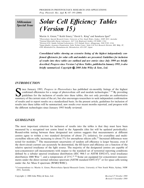
Solar Cell E ciency Tables (Version 15)Martin A.Green,1*Keith Emery,2David L.King 3and Sanekazu Igari 41Photovoltaics Special Research Centre,University of New South Wales,Sydney,NSW 2052,Australia2National Renewable Energy Laboratory,1617Cole Boulevard,Golden,CO 80401,USA3Division 6224,Sandia National Laboratories,1515Eubank Street,Albuquerque,NM 87185,USA 4Japan Quality Assurance Organization,Solar Techno Center,Solar Cell Test Research Division,HIC Bldg.2F,4598Murakushi-Cho,Hamamatsu-shi,Shizuoka-ken,431-1207,JapanConsolidated tables showing an extensive listing of the highest independently con-®rmed e ciencies for solar cells and modules are presented.Guidelines for inclusion of results into these tables are outlined and new entries since July 1999are brie¯y described.Progress since Version 1of these Tables,published in January 1993,is also brie¯y summarized.Copyright #2000John Wiley &Sons,Ltd.INTRODUCTIONSince January 1993,Progress in Photovoltaics has published six-monthly listings of the highest con®rmed e ciencies for a range of photovoltaic cell and module technologies.1±14By providing guidelines for the inclusion of results into these tables,this not only provides an authoritative summary of the current state of the art,but also encourages researchers to seek independent con®rmation of results and to report results on a standardized basis.In the present article,guidelines for inclusion of results into these tables will be summarized,new results over recent months reported,and progress with the di erent technologies since January 1993brie¯y reviewed.GUIDELINESThe most important criterion for inclusion of results into the tables is that they must have been measured by a recognized test centre listed in the Appendix (this list will be updated periodically).Round-robin testing between these designated test centres suggests that measurements at di erent centres agree to within a two standard deviation of about 2%(relative),for crystalline and multi-crystalline silicon cells,increasing to about 5%for amorphous silicon cells.15Increased di erences were noted for modules.15The measurement uncertainty of tandem cell e ciency is larger because,even if the short-circuit current can accurately be determined,the ®ll factor and e ciency are a function of the relative spectral irradiance of the light source.The majority of the designated centres are capable of non-concentrator cell measurements with respect to the standard set of terrestrial reporting conditions de®ned by a tabular spectral irradiance distribution (IEC 904-3or ASTM E892-87),total irradiance distribution 1000Wm À2,and a temperature of 258C.6±24Some are equipped for concentrator measure-ments under the direct normal reference spectrum (ASTM standard E891-87)17or for space cells testing under the Air Mass 0spectrum (WMO/WRC).PROGRESS IN PHOTOVOLTAICS:RESEARCH AND APPLICATIONSProg.Photovolt.Res.Appl.8,187±195(2000)*Correspondence to:Martin A.Green,Photovoltaics Special Research Centre,University of New South Wales,Sydney,NSW 2052,Australia.188M.A.GREEN ET AL.The area of the cell or module is an important parameter in determining e ciency.25It is also important that this area be measured by the test centre to an accuracy of better than0.5%.The areas used should conform to one of the three following provisional classi®cations:(i)Total area.This is the preferred area for reporting of results and equals the total projected area of thecell or module(the area that would be measured by taking a photograph of the device from a distance against a white background and measuring the area of the background shaded by the device).For the case of a cell attached to glass,the total area would be the area of the glass sheet.(ii)Aperture area.In this measurement,the device under test is masked so that the illuminated area is smaller than the total cell or module area,but all essential components of the device such as busbars,®ngers and interconnects lie within the masked area.(iii)Designated illumination area.In this case,the cell or module is masked to an area smaller than the total device area,but major cell or module components lie outside the masked area.For example,fora concentrator cell,the cell busbars would lie outside of the area designed for illumination and thisarea classi®cation would be the most appropriate.Results will be reported for cells and modules made from di erent semiconductors and for sub-categories within each semiconductor grouping(e.g.,crystalline,polycrystalline and thin®lm).Cell area must be at least1cm2for non-concentrating cells,although results for areas as low as0.25cm2will be eligible for concentrator cells.Given that cell and module e ciency normally decreases with increasing area,additional sub-categories will be included depending upon area.Although some¯exibility is desirable in this area,subcategory boundaries will be roughly at1cm2,10cm2and100cm2for non-concentrator cells,800cm2and3000cm2for modules,and0.25cm2,2cm2and20cm2for concentrator cells.NEW RESULTSHighest con®rmed cell results are reported in Tables I±III.Any changes in the tables from those previously published14are set in bold type.Table I summarizes the best measurements for cells and sub-modules,Table II shows the best results for modules and Table III shows the best results for concentrator cells and concentrator modules.Table IV contains what might be described as`notable exceptions'.While not conforming to the requirements to be recognized as a class record,the cells and modules in Table IV have notable characteristics that will be of interest to sections of the photovoltaic community.Two new results are reported in the present issue,both stemming from recent improvements in III±V monolithic tandem cells.Triple junction versions of these devices based on the GaInP/GaAs/Ge system are now in commercial production for space use.An e ciency of28.7%was demonstrated by a moderate area29.9cm2device fabricated by Spectrolab and measured by the National Renewable Energy Laboratory(Table I).This is the highest independently con®rmed e ciency for a one sun cell over4cm2 in area.A smaller triple junction cell(0.1cm2area)demonstrated32.3%e ciency at47suns concentra-tion(Table III),close to the highest ever for any photovoltaic device,and again the highest for a device of this size.Other results in the silicon and microcrystalline silicon areas are awaiting con®rmation and will be reported in the next issue of these tables.SUMMARY OF PROGRESSSince Version1of these tables was prepared almost exactly seven years ago,1there have been marked improvements in the best con®rmed results with several technologies.Some of the highlights are summarized below.In the bulk crystalline silicon area,the largest improvement has been in the module performance,driven by the demand for high performance modules for solar car racing.Con®rmed module performance has increased from18.2%to22.7%,representing25%relative improvement.Signi®cant but smallerimprovements also are documented for multicrystalline and supported ®lm devices,with even the basic 4cm 2silicon cell showing 7%relative improvement.In the III±V crystalline cell area,the major improvements have occurred in the monolithic tandem cell devices,with 2-junction devices surpassing 30%e ciency in 1996,and large area 3-junction devices now approaching similar e ciencies in commercial production.Table II.Con®rmed terrestrial module e ciencies measured under the global AM1.5spectrum (1000W/m 2)at a celltemperature of 258CClassi®cation a E c.b Area c V oc I sc FF d Test centre Description(%)(cm 2)(V)(A)(%)(and date)Si (crystalline)22.7+0.6778(da) 5.60 3.9380.3Sandia (9/96)UNSW/Gochermann 40Si (multicrystalline)15.3+0.41017(ap)14.6 1.3678.6Sandia (10/94)Sandia/HEM 41CIGSS 12.1+0.63651(ap)23.42 2.8367.9NREL (3/99)Siemens Solar 42CdTe10.5+0.21376(ap)34.910.65363.2JQA (2/99)Matsushita a-Si/a-SiGe/a-SiGe (tandem)e10.4+0.5905.1(ap)4.3533.28566.0NREL (10/98)USSC 43(a-Si/a-Si/a-Si :Ge)aCIGSS CuInGaSSe;a-Si amorphous silicon/hydrogen alloy;a-SiGe amorphous silicon/germanium/hydrogen alloy.bE c. e ciency.c (ap) aperture area;(da) designated illumination area.dFF ®ll factor.eLight soaked at NREL for 1000h at 508C,nominally 1-sun illumination.Table III.Terrestrial concentrator cell and module e ciencies measured under the direct beam AM1.5spectrum at acell temperature of 258CClassi®cationE c.a Area b Concentration c Test centres Description(%)(cm 2)(suns)(and date)Single cells GaAs 27.6+1.00.126(da)255Sandia (5/91)Spire 44GaInAsP 27.5+1.40.075(da)171NREL (2/91)NREL,Entech cover InP 24.3+1.20.075(da)99NREL (2/91)NREL,Entech cover 45Si26.8+0.8 1.60(da)96FhG-ISE (10/95)SunPower back-contact 46Si (large)21.6+0.720.0(da)11Sandia d (9/90)UNSW laser grooved 47GaAs (Si substrate)21.3+0.80.126(da)237Sandia (5/91)Spire 44InP (GaAs substrate)21.0+1.10.075(ap)88NREL (2/91)NREL,Entech cover 48Multijunction cells GaAs/GaSb 32.6+1.70.053(da)100Sandia d (10/89)Boeing,mechanical stack 49GaInP/GaAs/Ge 32.362.00.104(da)47NREL(9/99)Spectrolab,monolithicInP/GaInAs 31.8+1.60.063(da)50NREL (8/90)NREL,monolithic 3terminal 50GaAs/GaInAsP 30.2+1.50.053(da)40NREL (10/90)NREL,stacked 4terminal 50GaInP/GaAs 30.2+1.40.103(da)180Sandia (3/94)NREL,monolithic 2terminal 51GaAs/Si 29.6+1.50.317(da)350Sandia d (9/88)Varian/Stanford/Sandia,mech.stack 52Submodules GaAs/GaSb 25.1+1.441.4(ap)57Sandia (3/93)Boeing,3mech.stack units 53Modules Si20.3+0.81875(ap)80Sandia (4/89)Sandia/UNSW/ENTECH (12cells)54a E c. e ciency.b(da) designated illumination area;(ap) aperture area.cOne sun corresponds to an intensity of 1000Wm À2.d Measurements corrected from originally measured values due to Sandia recalibration in January 1991.190M.A.GREEN ET AL .192M.A.GREEN ET AL. In the compound semiconductor polycrystalline thin®lm area,the largest improvements have been obtained in the case of copper indium gallium selenide(CIGS)and related cells.The con®rmed perform-ance of1cm2devices has increased from13.7%to18.2%,a massive33%relative increase.Improvement at the module level has been9%relative.Almost the opposite has been the case for CdTe devices,where module performance has improved a massive30%relative,while the best con®rmed cell performance has not improved signi®cantly over this period.Similarly,in the amorphous silicon area,there has been little performance improvement con®rmed for 1cm2cells,although con®rmed small area tandem cell performance has improved by9%and stabilized module performance by17%.Some new categories have appeared since the®rst version of the tables representing emerging cell technologies.Two of note are nanocrystalline dye cells and thin®lm microcrystalline silicon cells on glass, where e ciencies of6.5%and10.1%,respectively,have been demonstrated for cells1±2cm2in area.DISCLAIMERWhile the information provided in the tables is provided in good faith,the authors,editors and publishers cannot accept direct responsibility for any errors or omissions.APPENDIXList of designated test centresEuropean Solar Test Installation(ESTI),CEC Joint Research Centre,21020Ispra(Varese),Italy. Contact:Dr Heinz Ossenbrink;Telephone:(39)332-789-196;Facsimile:(39)332-789-268;E-mail: jennifer.rundle@jrc.it/heinz.ossenbrink@(Terrestrial cells and modules)Fraunhofer-Institut fu r Solare Energiesysteme(Fraunhofer ISE),Oltmannsstrasse5,D-79100Freiburg, Germany.Contact:Dr Wilhelm Warta/Siegried Kunzelmann(cells);Georg Bopp(modules);Telephone:(49)761-4588-146;Facsimile:(49)761-4588-100;E-mail:wilhelm.warta@ise.fhg.de(Terrestrial and space cells and modules)Japan Quality Assurance Organization(JQA),Solar Techno Center,Solar Cell Test Research Division, HIC Bldg.2F,4598Murakushi-cho,Hanamatsu-shi,Shizuoka-ken,431-1207,Japan.Contact:Sanekazu Igari;Telephone:(81)53-484-4101;Facsimile:(81)53-484-4102;E-mail:sanekazu@carrot.ocn.ne.jp(Terrestrial cells and modules)NASA Lewis Research Center,MS302-1,21000Brookpark Road,Cleveland,OH44135,USA. Contact:Dr David Brinker,Senior Research Engineer;Telephone:(1)216-433-2236;Facsimile:(1)216-433-6106;E-mail:dbrinker@(AM0cell measurements)National Renewable Energy Laboratory,1617Cole Blvd.,Golden,CO80401,USA.Contact:Mr Keith Emery;Telephone:(1)303-384-6632;Facsimile:(1)303-384-6604;E-mail:keith_emery@(Terrestrial and concentrator cells and modules)Physikalisch-Technische Bundesanstalt,Bundesallee100,D-38116Braunschweig,Germany. Contact:Dr Ju rgen Metzdorf/Thomas Wittchen;Telephone:(49)531-592-4100/4181;Facsimile: (49)531-592-4105;E-mail:Juergen.Metzdoef@ptb.de(Terrestrial and AM0cells)SOLAR CELL EFFICIENCY TABLES193 Royal Aircraft Establishment,Defence Evaluation and Research Agency,Space Power Laboratory,X107 Building,Farnborough,Hampshire GU140LX,United Kingdom.Contact:C.Goodbody;Telephone:(44)1252-394-003;Facsimile:(44)1252-252-392-664;E-mail: cgoodbody@(Primarily AM0calibrations)Sandia National Laboratories,1515Eubank SE,Albuquerque,NM87123,USA.Contact:Mr David King;Dept.6219,MS-0752;Telephone:(1)505-844-8220;Facsimile: (1)505-844-6541;E-mail:dlking@(Terrestrial and concentrator cells and modules)REFERENCES1.M.A.Green and K.Emery,`Solar cell e ciency tables',Progr.Photovolt.,1,25±29(1993).2.M.A.Green and K.Emery,`Solar cell e ciency tables(version2)',Progr.Photovolt.,1,225±228(1993).3.M.A.Green and K.Emery,`Solar cell e ciency tables(version3)',Progr.Photovolt.,2,27±34(1994).4.M.A.Green and K.Emery,`Solar cell e ciency tables(version4)',Progr.Photovolt.,2,231±234(1994).5.M.A.Green,K.Emery,K.Bu cher and D.L.King,`Solar cell e ciency tables(version5)',Progr.Photovolt.,3,51±55(1995).6.M.A.Green,K.Emery,K.Bu cher and D.L.King,`Solar cell e ciency tables(version6)',Progr.Photovolt.,3,229±233(1995).7.M.A.Green,K.Emery,K.Bu cher and D.L.King,`Solar cell e ciency tables(version7)',Progr.Photovolt.,4,59±62(1996).8.M.A.Green,K.Emery,K.Bu cher,D.L.King and S.Igari,`Solar cell e ciency tables(version8)',Progr.Photovolt.,4,321±325(1996).9.M.A.Green,K.Emery,K.Bu cher,D.L.King and S.Igari,`Solar cell e ciency tables(version9)',Progr.Photovolt.,5,51±54(1997).10.M.A.Green,K.Emery,K.Bu cher,D.L.King and S.Igari,`Solar cell e ciency tables(version10)',Progr.Photovolt.,5,265±268(1997).11.M.A.Green,K.Emery,K.Bu cher,D.L.King and S.Igari,`Solar cell e ciency tables(version11)',Progr.Photovolt.,6,35±42(1998).12.M.A.Green,K.Emery,K.Bu cher,D.L.King and S.Igari,`Solar cell e ciency tables(version12)',Progr.Photovolt.,6,265±270(1998).13.M.A.Green,K.Emery,K.Bu cher,D.L.King and S.Igari,`Solar cell e ciency tables(version13)',Progr.Photovolt.,7,31±38(1999).14.M.A.Green,K.Emery,K.Bu cher,D.L.King and S.Igari,`Solar cell e ciency tables(version14)',Progr.Photovolt.,7,321±326(1999).15.J.Metzdorf,T.Wittchen,K.Heidler,K.Dehne,R.Shimokawa,F.Nagamine,H.Ossenbrink,L.Fornarini,C.Goodbody,M.Davies,K.Emery and R.DeBlasio,Objectives and results of the PEP'87round-robin calibration of reference solar cells and modules,in Conf.Record,21st IEEE Photovoltaic Specialists Conf.,Kissimimee,May, 1990,pp.952±959.16.Standard for Terrestrial Solar Spectral Irradiance Tables at Air Mass1.5for a378Tilted Surface,ASTMStandard E892,Vol.12.02,Philadelphia,PA.17.Standard for Terrestrial Direct Normal Solar spectral Irradiance Tables for Air Mass1.5,ASTM StandardE891,Vol.12.02,Philadelphia,PA.18.Measurement Principles for Terrestrial PV Solar Devices with Reference Spectral Irradiance Data,InternationalElectrochemical Commission Standard904-3,1989.19.Photovoltaic Devices Part1Measurement of Photovoltaic Current±Voltage Characteristics,InternationalElectrochemical Commission Standard904-1,1989.20.Standard Methods of Testing Electrical Performance of Non-Concentrator Terrestrial Photovoltaic Modulesand Arrays Using Reference Cells,ASTM Standard E1036,Philadelphia,PA.21.Standard Methods of Testing Electrical Performance of1Photovoltaic Cells Using Reference Cells,ASTMStandard E948,Vol.12.02,Philadelphia,PA.194M.A.GREEN ET AL.22.Standard Procedures for Terrestrial Photovoltaic Measurements,Commission of The European Community,CEC101,Issue2,EUR7078,EN,1981.23.K.A.Emery,C.R.Osterwald and C.V.Wells,Uncertainty analysis of photovoltaic e ciency measurements,Proc.19th IEEE Photovoltaic Specialists Conf.,New Orleans,LA,4±8May,1987,pp.153±159.24.K.Heidler and J.Beier,Uncertainty analysis of PV e ciency measurements with a solar simulator:spectralmismatch,non-uniformity and other sources of error,Proc.8th European Solar Energy Conf.,Florence,Italy, 9±12May,1988,pp.554±559.25.K.Emery and C.Osterwald,`E ciency measurements and other performance-rating methods',in CurrentTopics in Photovoltaics,Chap.4,Eds.T.Coutts and J.Meakin,Vol.3,pp.301±350,Academic Press,New York, 1988.26.J.Zhao,A.Wang,M.Green and F.Ferrazza,`Novel19.8%e cient`honeycomb'textured multicrystalline and24.4%monocrystalline silicon solar cell',Appl.Phys.Lett.,73,1991±1993(1998).27.Y.Bai,D.H.Ford,J.Rand and A.Barnett,16.6%e cient silicon-®lm2polycrystalline silicon solar cell,inConf.Record,26th IEEE Photovoltaic Specialists Conf.,Anaheim,September/October,1997,pp.35±38. 28.R.P.Gale,R.W.McClelland,D.B.Dingle,J.V.Gormley,R.M.Burgess,N.P.Kim,R.A.Mickelsen and B.J.Stanbery,High-e ciency GaAs/CuInSe2and AlGaAs/CuInSe2thin-®lm tandem solar cells,in Conf.Record, 21st IEEE Photovoltaic Specialists Conf.,Kissimimee,May,1990,pp.53±57.29.R.Venkatasubramanian,B.C.O'Quinn,J.S.Hills,P.R.Sharps,M.L.Timmons,J.A.Hutchby,H.Field,A.Ahrenkiel and B.Keyes,18.2%(AM1.5)e cient GaAs solar cell on optical-grade polycrystalline Ge substrate, in Conf.Record,25th IEEE Photovoltaic Specialists Conf.,Washington,May,1997,pp.31±36.30.C.J.Keavney,V.E.Haven and S.M.Vernon,Emitter structures in MOCVD InP solar cells,in Conf.Record,21st IEEE PHotovoltaic Specialists Conf.,Kissimimee,May,1990,pp.141±144.31.H.Ohyama,T.Aramoto,S.Kumazawa,H.Higuchi,T.Arita,S.Shibutani,T.Nishio,J.Nakajima,M.Tsuji,A.Hanafusa,T.Hibino,K.Omura and M.Murozono,16.0%e cient thin-®lm CdS/CdTe solar cells,in Conf.Record,26th IEEE Photovoltaic Specialists Conf.,Anaheim,September/October,1997,pp.343±346.32.D.Bonnet,H.Richter and K.Ja ger,The CTS thin®lm solar moduleÐcloser to production,in Conf.Record,13th European Photovoltaic Solar Energy Conf.,Nice,October,1995,pp.1456±1461.33.M.A.Contreras,B.Egaas,K.Ramanathan,J.Hiltner,A.Swartzlander,F.Hasoon and R.Nou®,`Progresstoward20%e ciency in Cu(In,Ga)Se polycrystalline thin-®lm solar cell',Progr.Photovolt.,7(this issue). 34.N.F.Cooray,K.Kushiya,A.Fujimaki,I.Sugimaya,T.Miura,D.Okumura,M.Sato,M.Ooshita and O.Yamase,Large area ZnO®lms optimized for graded band-gap Cu(InGa)Se2-based thin-®lm mini-modules,in Tech.Digest,Init.PVSEC-9,Miyasaki,November,1996,pp.597±598.35.S.Okamoto,T.Takahama,Y.Hishikawa,S.Tsuge,M.Nishikune,N.Nakamura,S.Tsuda,H.Nishiwaki,S.Nakano and Y.Kuwano,Improvement in a-Si:H and a-SiC:H for high-e ciency solar cells using hydrogen plasma treatment,in Conf.Record,11th European Photovoltaic Solar Energy Conf.,Montreux,October,1992, pp.537±540.36.Y.Hishikawa,M.Isomura,S.Okamoto,H.Hashimoto and S.Tsuda,E ects of the i-layer properties andimpurity on the performance of a-Si solar cells,in Tech.Digest,Int.PVSEC-7,Nagoya,November,1993, pp.29±32.37.M.Ohmori,T.Takamoto,E.Ikeda and H.Kurita,High e ciency InGaP/GaAs tandem solar cells,in Tech.Digest,Int.PVSEC-9,Miyazaki,Japan,November,1996,pp.525±528.38.K.Mitchell,C.Eberspacher,J.Ermer and D.Pier,Single and tandem junction CuInSe2cell and moduletechnology,in Conf.Record,20th IEEE Photovoltaic Specialists Conf.,Las Vegas,September,1988, pp.1384±1389.39.J.Yang,A.Banerjee,S.Sugiyama and S.Guha,Recent progress in amorphous silicon alloy leading to13%stable cell e ciency,in Conf.Record,26th IEEE Photovoltaic Specialists Conf.,Anaheim,September/October, 1997,pp.563±568.40.J.H.Zhao,A.Wang,F.Yun,G.Zhang,D.M.Roche,S.R.Wenham and M.A.Green,`20,000PERL siliconcells for the`1996World Solar Challenge'solar car race',Progr.Photovolt.,5,269±276(1997).41.D.L.King,W.K.Schubert and T.D.Hund,World's®rst15%e ciency multicrystalline silicon modules,Conf.Record,1st World Conf.on Photovoltaic Energy Conversion,Hawaii,December,1994,pp.1660±1662.42.R.R.Gay,Status and prospects for CIS-based photovoltaics,in Tech.Digest,Int.PVSEC-9,Miyazaki,1996,pp.149±152.43.J.Yang,A.Banerjee,T.Glatfelter,K.Ho man,X.Xu and S.Guha,Progress in triple-junction amorphoussilicon-based alloy solar cells and modules using hydrogen dilution,in Conf.Record,1st World Conf.Photovoltaic Energy Conversion,Hawaii,December,1994,pp.380±385.SOLAR CELL EFFICIENCY TABLES195 44.S.M.Vernon,S.P.Tobin,V.E.Haven,L.M.Geo roy and M.M.Sanfacon,High-e ciency concentratorcells from GaAs on Si,in Conf.Record,22nd IEEE Photovoltaic Specialists Conf.,Las Vegas,October,1991, pp.353±357.45.J.S.Ward,M.W.Wanlass,T.J.Coutts,K.A.Emery and C.R.Osterwald,InP concentrator solar cells,in Conf.Record,22nd IEEE Photovoltaic Specialists Conf.,Las Vegas,October,1991,pp.365±370.46.P.J.Verlinden,R.M.Swanson,R.A.Crane,K.Wickham and J.Perkins,A26.8%e cient concentrator point-contact solar cell,in Conf.Record,13th European Photovoltaic Solar Energy Conf.,Nice,October,1995, pp.1582±1585.47.F.Zhang,S.R.Wenham and M.A.Green,`Large area,concentrator buried contact solar cells',IEEE Trans.onElect.Devs.,42,144±149(1995).48.M.W.Wanlass,T.J.Coutts,J.S.Ward and K.A.Emery,High-e ciency heteroepitaxial InP solar cells,inConf.Record,21st IEEE Photovoltaic Specialists Conf.,Kissimimee,May,1990,pp.159±165.49.L.M.Frass,J.E.Avery,V.S.Sundaram,V.T.Kinh,T.M.Davenport,J.W.Yerkes,J.M.Gee and K.A.Emery,Over35%e cient GaAs/GaSb stacked concentrator cell assemblies for terrestrial applications,in Conf.Record,21st IEEE Photovoltaic Specialists Conf.,Kissimimee,May,1990,pp.190±195.50.M.W.Wanlass,T.J.Coutts,J.S.Ward,K.A.Emery,T.A.Gessert and C.R.Osterwald,Advanced high-e ciency concentrator tandem solar cells,in Conf.Record,21st IEEE Photovoltaic Specialists Conf.,Kissimimee,May,1990,pp.38±45.51.D.J.Friedman,S.R.Kurtz,K.A.Bertness,A.E.Kibbler,C.Kramer,J.M.Olson,D.L.King,B.R.Hansenand J.K.Snyder,`30.2%e cient GaInP/GaAs monolithic two-terminal tandem concentrator cells',Progr.Photovolt.,3,47±50(1995).52.J.M.Gee and G.F.Virshup,A30%-e cient GaAs/Silicon mechanically stacked,multijunction concentratorsolar cell,in Conf.Record,20th IEEE Photovoltaic Specialists Conf.,Las Vegas,September,1988,pp.754±758.53.M.F.Piszczor,D.J.Brinker,D.J.Flood,J.E.Avery,L.M.Fraas,E.S.Fairbanks,J.W.Yerkes and M.J.O'Neill,A high-performance photovoltaic concentrator array:the mini-dome Fresnel lens concentrator with 30%e cient GaAs/GaSb tandem cells,in Conf.Record,22nd IEEE Photovoltaic Specialists Conf.,Las Vegas,October,1991,pp.1485±1489.54.C.J.Chiang and E.H.Richards,A20%e cient photovoltaic concentrator module,in Conf.Record,21st IEEEPhotovoltaic Specialists Conf.,Kissimimee,May,1990,pp.861±863.55.J.Knobloch,S.W.Glunz,D.Biro,W.Warta,E.Scha er and W.Wettling,Solar cells with e ciencies above21%processed from Czochralski grown silicon,in Conf.Record,25th IEEE Photovoltaic Specialists Conf., Washington,May,1996,pp.405±408.56.A.Wang,J.Zhao,S.R.Wenham and M.A.Green,`21.5%e cient thin silicon solar cell',Progr.Photovolt.,4,55±58(1996).57.C.Hebling,S.W.Glunz,J.O.Schumacher and J.Knobloch,High-e ciency(19.2%)silicon thin-®lm solar cellswith interdigitated emitter and base-front-contact,in Conf.Record,14th European Photovoltaic Solar Energy Conf.,Barcelona,July,1997,pp.2318±2323.utenschlager,F.Lutz,C.Schetter,U.Schubert and R.Schindler,MC-silicon solar cells with417%e ciency,in Conf.Record,26th IEEE Photovoltaic Specialists Conf.,Anaheim,September,1997,pp.7±12.59.H.Nakaya,M.Nishida,Y.Takeda,S.Moriuchi,T.Tonegawa,T.Machida and T.Nunoi,`Polycrystallinesilicon solar cells with v-grooved surface',Solar Energy Mat.Solar Cells,34,219±225(1994).60.C.Hebling,S.Reber,K.Schmidt,R.Lu dermann and F.Lutz,Oriented recrystallization of silicon layers ofsilicon thin-®lm solar cells,in Conf.Record,26th IEEE Photovoltaic Specialists Conf.,Anaheim,September, 1997,pp.623±626.61.K.Yamamoto,M.Yoshimi,T.Suzuki,Y.Tawada,T.Okamoto and A.Nakajima,Thin®lm poly-si solar cell onglass substrate fabricated at low temperature,presented at MRS Spring Meeting,San Francisco,April,1998.62.Y.C.M.Yeh,C.Chang,F.Ho and H.Yoo,Large scale,high e ciency GaAs/Ge cell production,in Conf.Record,21st IEEE Photovoltaic Specialists Conf.,Kissimimee,May,1990,pp.79±83.63.R.R.Schmit,J.S.Reynolds,J.K.Arch and G.D.Stevens,The e ect of silicon purity on spheral Solar2cellprocessing and performance,in Conf.Record,24th IEEE Photovoltaic Specialists Conf.,Hawaii,December, 1994,pp.1603±1606.64.H.S.Ullal,K.Zweibel and B.G.von Roedern,Current status of polycrystalline thin-®lm technologies,in Conf.Record,26th IEEE Photovoltaic Specialists Conf.,Anaheim,September,1997,pp.301±305.。
一种用于治疗脉络膜新生血管的多肽纳米材料及其制备方法和应用[

(19)中华人民共和国国家知识产权局(12)发明专利申请(10)申请公布号 (43)申请公布日 (21)申请号 202011261144.4(22)申请日 2020.11.12(71)申请人 国家纳米科学中心地址 100190 北京市海淀区中关村北一条11号(72)发明人 王磊 王浩 张扩 (74)专利代理机构 北京品源专利代理有限公司11332代理人 巩克栋(51)Int.Cl.C07K 7/08(2006.01)C07K 7/06(2006.01)C07K 19/00(2006.01)B82Y 5/00(2011.01)B82Y 40/00(2011.01)A61K 47/64(2017.01)A61K 47/54(2017.01)A61P 9/00(2006.01)(54)发明名称一种用于治疗脉络膜新生血管的多肽纳米材料及其制备方法和应用(57)摘要本发明提供一种用于治疗脉络膜新生血管的多肽纳米材料及其制备方法和应用。
所述多肽纳米材料包括通过酰胺键相连的疏水单元、组装单元和靶向单元;所述靶向单元包括靶向新生血管内皮细胞的多肽序列,且所述多肽序列与血管内皮生长因子共受体特异性结合。
本发明提供的多肽纳米材料具有靶向新生血管内皮细胞的作用,并且通过配体‑受体相互作用与血管内皮生长因子共受体结合,并自组装形成纳米纤维,包裹在内皮细胞表面并占据了血管内皮生长因子共受体,阻断了其余血管内皮生长因子结合的信号通路,抑制内皮细胞的迁移,抑制新生血管生成,所述多肽纳米材料为脉络膜新生血管的治疗提供了可靠的靶向治疗方法。
权利要求书3页 说明书10页 附图8页CN 112409455 A 2021.02.26C N 112409455A1.一种用于治疗脉络膜新生血管的多肽纳米材料,其特征在于,所述多肽纳米材料包括通过酰胺键相连的疏水单元、组装单元和靶向单元;所述靶向单元包括靶向新生血管内皮细胞的多肽序列,且所述多肽序列与血管内皮生长因子共受体特异性结合。
基因插入使皮肤干细胞转变成类胚胎干细胞
基因插入使皮肤干细胞转变成类胚胎干细胞
薛惠文;章静波
【期刊名称】《基础医学与临床》
【年(卷),期】2008(28)2
【总页数】1页(P163-163)
【关键词】类胚胎干细胞;皮肤干细胞;基因插入;皮肤细胞;科学家
【作者】薛惠文;章静波
【作者单位】
【正文语种】中文
【中图分类】R329-33;R318
【相关文献】
1.印迹基因修饰使孤雌胚胎干细胞获得四倍体补偿能力 [J], 李旭;彭柯力;张金鑫;高倩;张文豪;滑若彤;帅领
2.纤维母细胞生长因子依赖的鼠诱导性多潜能干细胞具有类胚胎干细胞多能性 [J], 田丽
3.科学家利用人体皮肤细胞研制出类胚胎干细胞 [J],
4.科学家利用人体皮肤细胞研制出类胚胎干细胞 [J],
5.科学家首次利用人体皮肤细胞培育出类胚胎干细胞 [J],
因版权原因,仅展示原文概要,查看原文内容请购买。
日科学家找到制作安全万能细胞的新基因
日科学家找到制作安全万能细胞的新基因
佚名
【期刊名称】《企业技术开发》
【年(卷),期】2011()7
【摘要】据《日本经济新闻》等多家媒体2011年6月9日报道,京都大学万能细胞(ips细胞)发明人山中伸弥教授领导的研究团队找到一种名为G-isI的新基因,与山中教授自己发现的四个基因(又被称为"山中基因")结合,制作安全性能高的万能细胞取得成功,
【总页数】1页(P165-165)
【关键词】安全性能;新基因;细胞;制作;科学家;《日本经济新闻》;京都大学;发明人【正文语种】中文
【中图分类】Q78
【相关文献】
1.我科学家育出人胚胎干细胞·白血病重要致病因素被发现·生殖科学的新成果·吉林大学首创新型视觉导航AGV·巴西科学家破解相对论引出的著名悖论·乙肝病毒基因组新编码基因被破译 [J],
2.日科学家用淋巴细胞合成“万能细胞” [J],
3.中国科学家找到新的基因编辑工具 [J], ;
4.科学家找到治疗耳聋新方法修复内耳细胞基因有望治疗耳聋 [J], 李学华
5.科学家找到令癌细胞基因沉默新方法 [J],
因版权原因,仅展示原文概要,查看原文内容请购买。
光伏发电英文文献Ultra-High Efficiency Photovoltaic
Ultra-High Efficiency Photovoltaic Cells for Large Scale Solar Power GenerationYoshiaki NakanoAbstract The primary targets of our project are to dras-tically improve the photovoltaic conversion efficiency and to develop new energy storage and delivery technologies. Our approach to obtain an efficiency over40%starts from the improvement of III–V multi-junction solar cells by introducing a novel material for each cell realizing an ideal combination of bandgaps and lattice-matching.Further improvement incorporates quantum structures such as stacked quantum wells and quantum dots,which allow higher degree of freedom in the design of the bandgap and the lattice strain.Highly controlled arrangement of either quantum dots or quantum wells permits the coupling of the wavefunctions,and thus forms intermediate bands in the bandgap of a host material,which allows multiple photon absorption theoretically leading to a conversion efficiency exceeding50%.In addition to such improvements, microfabrication technology for the integrated high-effi-ciency cells and the development of novel material systems that realizes high efficiency and low cost at the same time are investigated.Keywords Multi-junctionÁQuantum wellÁConcentratorÁPhotovoltaicINTRODUCTIONLarge-scale photovoltaic(PV)power generation systems, that achieve an ultra-high efficiency of40%or higher under high concentration,are in the spotlight as a new technology to ease drastically the energy problems.Mul-tiple junction(or tandem)solar cells that use epitaxial crystals of III–V compound semiconductors take on the active role for photoelectric energy conversion in such PV power generation systems.Because these solar cells operate under a sunlight concentration of5009to10009, the cost of cells that use the epitaxial crystal does not pose much of a problem.In concentrator PV,the increased cost for a cell is compensated by less costly focusing optics. The photons shining down on earth from the sun have a wide range of energy distribution,from the visible region to the infrared region,as shown in Fig.1.Multi-junction solar cells,which are laminated with multilayers of p–n junctions configured by using materials with different band gaps,show promise in absorbing as much of these photons as possible,and converting the photon energy into elec-tricity with minimum loss to obtain high voltage.Among the various types of multi-junction solar cells,indium gallium phosphide(InGaP)/gallium arsenide(GaAs)/ger-manium(Ge)triple-junction cells that make full use of the relationship between band gaps and diverse lattice con-stants offered by compound semiconductors have the advantage of high conversion efficiency because of their high-quality single crystal with a uniform-size crystal lat-tice.So far,a conversion efficiency exceeding41%under conditions where sunlight is concentrated to an intensity of approximately5009has been reported.The tunnel junction with a function equivalent to elec-trodes is inserted between different materials.The positive holes accumulated in the p layer and the electrons in the adjacent n layer will be recombined and eliminated in the tunnel junction.Therefore,three p–n junctions consisting of InGaP,GaAs,and Ge will become connected in series. The upper limit of the electric current is set by the mini-mum value of photonflux absorbed by a single cell.On the other hand,the sum of voltages of three cells make up the voltage.As shown in Fig.1,photons that can be captured in the GaAs middle cell have a smallflux because of the band gap of each material.As a result,the electric currentoutputAMBIO2012,41(Supplement2):125–131 DOI10.1007/s13280-012-0267-4from the GaAs cell theoretically becomes smaller than that of the others and determines the electric current output of the entire tandem cell.To develop a higher efficiency tandem cell,it is necessary to use a material with a band gap narrower than that of GaAs for the middle cell.In order to obtain maximum conversion efficiency for triple-junction solar cells,it is essential to narrow down the middle cell band gap to 1.2eV and increase the short-circuit current density by 2mA/cm 2compared with that of the GaAs middle cell.When the material is replaced with a narrower band gap,the output voltage will drop.However,the effect of improving the electric current balance out-performs this drop in output voltage and boosts the effi-ciency of the entire multi-junction cell.When a crystal with such a narrow band gap is grown on a Ge base material,lattice relaxation will occur in the middle of epitaxial crystal growth because the lattice constants of narrower band-gap materials are larger than that of Ge (as shown in Fig.2).As a result,the carrier transport properties will degrade due to dislocation.Researchers from the international research center Solar Quest,the University of Tokyo,aim to move beyond such material-related restrictions,and obtain materials and structures that have effective narrow band gaps while maintaining lattice matching with Ge or GaAs.To achieve this goal,we have taken three approaches as indicated in Fig.3.These approaches are explained in detail below.DILUTE NITROGEN-ADDED BULK CRYSTAL Indium gallium nitride arsenide (InGaNAs)is a bulk material consists of InGaAs,which contains several percent of nitrogen.InGaNAs has a high potential for achieving a narrow band gap while maintaining lattice matching with Ge or GaAs.However,InGaNAs has a fatal problem,that is,a drop in carrier mobility due to inhomogeneousdistribution of nitrogen (N).To achieve homogeneous solid solution of N in crystal,we have applied atomic hydrogen irradiation in the film formation process and addition of a very small amount of antimony (Sb)(Fig.3).The atomic hydrogen irradiation technology and the nitrogen radical irradiation technology for incorporating N efficiently into the crystal can be achieved only through molecular beam epitaxy (MBE),which is used to fabricate films under high vacuum conditions.(Nitrogen radical irradiation is a technology that irradiates the surface of a growing crystal with nitrogen atoms that are resolved by passing nitrogen through a plasma device attached to the MBE system.)Therefore,high-quality InGaNAs has been obtained only by MBE until now.Furthermore,as a small amount of Sb is also incorporated in a crystal,it is nec-essary to control the composition of five elements in the crystal with a high degree of accuracy to achieve lattice matching with Ge or GaAs.We have overcome this difficulty by optimizing the crystal growth conditions with high precision and devel-oped a cell that has an InGaNAs absorption layer formed on a GaAs substrate.The short-circuit current has increased by 9.6mA/cm 2for this cell,compared with a GaAs single-junction cell,by narrowing the band gap down to 1.0eV.This technology can be implemented not only for triple-junction cells,but also for higher efficiency lattice-matched quadruple-junction cells on a Ge substrate.In order to avoid the difficulty of adjusting the compo-sition of five elements in a crystal,we are also taking an approach of using GaNAs with a lattice smaller than that of Ge or GaAs for the absorption layer and inserting InAs with a large lattice in dot form to compensate for the crystal’s tensile strain.To make a solid solution of N uniformly in GaNAs,we use the MBE method for crystal growth and the atomic hydrogen irradiation as in the case of InGaNAs.We also believe that using 3D-shaped InAs dots can effectively compensate for the tensile strainthatFig.1Solar spectrum radiated on earth and photon flux collected by the top cell (InGaP),middle cell (GaAs),and bottom cell (Ge)(equivalent to the area of the filled portions in the figure)occurs in GaNAs.We have measured the characteristics of a single-junction cell formed on a GaAs substrate by using a GaNAs absorption layer with InAs dots inserted.Figure 4shows that we were able to succeed in enhancing the external quantum efficiency in the long-wavelength region (corresponding to the GaNAs absorp-tion)to a level equal to GaAs.This was done by extending the absorption edge to a longer wavelength of 1200nm,and increasing the thickness of the GaNAs layer by increasing the number of laminated InAs quantum dot layers.This high quantum efficiency clearly indicates that GaNAs with InAs dots inserted has the satisfactory quality for middle cell material (Oshima et al.2010).STRAIN-COMPENSATED QUANTUM WELL STRUCTUREIt is extremely difficult to develop a narrow band-gap material that can maintain lattice matching with Ge orGaAs unless dilute nitrogen-based materials mentioned earlier are used.As shown in Fig.2,the conventionally used material InGaAs has a narrower band gap and a larger lattice constant than GaAs.Therefore,it is difficult to grow InGaAs with a thickness larger than the critical film thickness on GaAs without causing lattice relaxation.However,the total film thickness of InGaAs can be increased as an InGaAs/GaAsP strain-compensated multi-layer structure by laminating InGaAs with a thickness less than the critical film thickness in combination with GaAsP that is based on GaAs as well,but has a small lattice constant,and bringing the average strain close to zero (Fig.3.).This InGaAs/GaAsP strain-compensated multilayer structure will form a quantum well-type potential as shown in Fig.5.The narrow band-gap InGaAs layer absorbs the long-wavelength photons to generate electron–hole pairs.When these electron–hole pairs go over the potential bar-rier of the GaAsP layer due to thermal excitation,the electrons and holes are separated by a built-in electricfieldFig.2Relationship between band gaps and lattice constants of III–V-based and IV-based crystalsto generate photocurrent.There is a high probability of recombination of electron–hole pairs that remain in the well.To avoid this recombination,it is necessary to take out the electron–hole pairs efficiently from the well and transfer them to n-type and p-type regions without allowing them to be recaptured into the well.Designing thequantumFig.3Materials and structures of narrow band-gap middle cells being researched by thisteamFig.4Spectral quantum efficiency of GaAs single-junction cell using GaNAs bulk crystal layer (inserted with InAs dots)as the absorption layer:Since the InAs dot layer and the GaNAs bulk layer are stacked alternately,the total thickness of GaNAs layers increases as the number of stacked InAs dot layers is increased.The solid line in the graph indicates the data of a reference cell that uses GaAs for its absorption layer (Oshima et al.2010)well structure suited for this purpose is essential for improving conversion efficiency.The high-quality crystal growth by means of the metal-organic vapor phase epitaxy (MOVPE)method with excellent ability for mass production has already been applied for InGaAs and GaAsP layers in semiconductor optical device applications.Therefore,it is technologically quite possible to incorporate the InGaAs/GaAsP quantum well structure into multi-junction solar cells that are man-ufactured at present,only if highly accurate strain com-pensation can be achieved.As the most basic approach related to quantum well structure design,we are working on fabrication of super-lattice cells with the aim of achieving higher efficiency by making the GaAsP barrier layer as thin as possible,and enabling carriers to move among wells by means of the tunnel effect.Figure 6shows the spectral quantum effi-ciency of a superlattice cell.In this example,the thickness of the GaAsP barrier layer is 5nm,which is not thin enough for proper demonstration of the tunnel effect.When the quantum efficiency in the wavelength range (860–960nm)that corresponds to absorption of the quan-tum well is compared between a cell,which has a con-ventionally used barrier layer and a thickness of 10nm or more,and a superlattice cell,which has the same total layer thickness of InGaAs,the superlattice cell demonstrates double or higher quantum efficiency.This result indicates that carrier mobility across quantum wells is promoted by even the partial use of the tunnel effect.By increasing the P composition in the GaAsP layer,the thickness of well (or the In composition)can be increased,and the barrier layer thickness can be reduced while strain compensation is maintained.A cell with higher quantum efficiency can befabricated while extending the absorption edge to the long-wavelength side (Wang et al.2010,2012).GROWTH TECHNIQUE FOR STRAIN-COMPENSATED QUANTUM WELLTo reduce the strain accumulated in the InGaAs/GaAsP multilayer structure as close to zero as possible,it is nec-essary to control the thickness and atomic content of each layer with high accuracy.The In composition and thickness of the InGaAs layer has a direct effect on the absorption edge wavelength and the GaAsP layer must be thinned to a satisfactory extent to demonstrate fully the tunnel effect of the barrier layer.Therefore,it is desirable that the average strain of the entire structure is adjusted mainly by the P composition of the GaAsP layer.Meanwhile,for MOVPE,there exists a nonlinear rela-tionship between the P composition of the crystal layer and the P ratio [P/(P ?As)]in the vapor phase precursors,which arises from different absorption and desorption phenomena on the surface.As a result,it is not easy to control the P composition of the crystal layer.To break through such a difficulty and promote efficient optimiza-tion of crystal growth conditions,we have applied a mechanism to evaluate the strain of the crystal layer during growth in real time by sequentially measuring the curvature of wafers during growth with an incident laser beam from the observation window of the reactor.As shown in Fig.7,the wafer curvature during the growth of an InGaAs/GaAsP multilayer structure indicates a periodic behavior.Based on a simple mechanical model,it has become clear that the time changes ofwaferFig.5Distribution of potential formed by the InGaAs/GaAsP strain-compensated multilayer structure:the narrow band-gap InGaAs layer is sandwiched between wide band-gap GaAsP layers and,as a result,it as quantum well-type potential distribution.In the well,electron–hole pairs are formed by absorption of long-wavelength photons and at the same time,recombination of electrons and holes takes place.The team from Solar Quest is focusing on developing a superlattice structure with the thinnest GaAsP barrier layercurvature are proportionate to the strain of the crystal layer relative to a substrate during the growing process.One vibration cycle of the curvature is same as the growth time of an InGaAs and GaAsP pair (Sugiyama et al.2011).Therefore,the observed vibration of the wafer curvature reflects the accumulation of the compression strain that occurs during InGaAs growth and the release of the strain that occurs during GaAsP growth.When the strain is completely compensated,the growth of the InGaAs/GaAsP pair will cause this strain to return to the initial value and the wafer curvature will vibrate with the horizontal line as the center.As shown in Fig.7,strain can be compensated almost completely by adjusting the layer structure.Only by conducting a limited number of test runs,the use of such real-time observation technology of the growth layer enables setting the growth conditions for fabricating the layer structure for which strain has been compensated with highaccuracy.Fig.6Spectral quantum efficiency of GaAs single-junction cell using InGaAs/GaAsP superlattice as theabsorption layer:This structure consists of 60layers of InGaAs quantum wells.The graph also shows data of a reference cell that uses GaAs for its absorption layer (Wang et al.2010,2012)Fig.7Changes in wafer curvature over time during growth of the InGaAs/GaAsP multilayer structure.This graph indicates the measurement result and the simulation result of the curvature based on the layer structure(composition ?thickness)obtained by X-ray diffraction.Since compressive strain is applied during InGaAs growth,the curvature decreases as time passes.On the other hand,since tensile strain is applied during GaAsP growth,the curvature changes in the oppositedirection (Sugiyama et al.2011)FUTURE DIRECTIONSIn order to improve the conversion efficiency by enhancing the current matching of multi-junction solar cells using III–V compound semiconductors,there is an urgent need to create semiconductor materials or structures that can maintain lattice matching with Ge or GaAs,and have a band gap of1.2eV.As for InGaNAs,which consists of InGaAs with several percent of nitrogen added,we have the prospect of extending the band edge to1.0eV while retaining sufficient carrier mobility for solar cells by means of atomic hydrogen irradiation and application of a small quantity of Sb during the growth process.In addition,as for GaNAs bulk crystal containing InAs dots,we were able to extend the band edge to1.2eV and produce a high-quality crystal with enoughfilm thickness to achieve the quantum efficiency equivalent to that of GaAs.These crystals are grown by means of MBE. Therefore,measures that can be used to apply these crys-tals for mass production,such as migration to MOVPE, will be investigated after demonstrating their high effi-ciency by embedding these crystals into multi-junction cells.As for the InGaAs/GaAsP strain-compensated quantum well that can be grown using MOVPE,we are working on the development of a thinner barrier layer while compen-sating for the strain with high accuracy by real-time observation of the wafer curvature.We have had the prospect of achieving a quantum efficiency that will sur-pass existing quantum well solar cells by promoting the carrier transfer within the multilayer quantum well struc-ture using the tunnel effect.As this technology can be transferred quite easily to the existing multi-junction solar cell fabrication process,we strongly believe that this technology can significantly contribute to the efficiency improvement of the latest multi-junction solar cells. REFERENCESOshima,R.,A.Takata,Y.Shoji,K.Akahane,and Y.Okada.2010.InAs/GaNAs strain-compensated quantum dots stacked up to50 layers for use in high-efficiency solar cell.Physica E42: 2757–2760.Sugiyama,M.,K.Sugita,Y.Wang,and Y.Nakano.2011.In situ curvature monitoring for metalorganic vapor phase epitaxy of strain-balanced stacks of InGaAs/GaAsP multiple quantum wells.Journal of Crystal Growth315:1–4.Wang,Y.,Y.Wen,K.Watanabe,M.Sugiyama,and Y.Nakano.2010.InGaAs/GaAsP strain-compensated superlattice solar cell for enhanced spectral response.In Proceedings35th IEEE photovoltaic specialists conference,3383–3385.Wang,Y.P.,S.Ma,M.Sugiyama,and Y.Nakano.2012.Management of highly-strained heterointerface in InGaAs/GaAsP strain-balanced superlattice for photovoltaic application.Journal of Crystal Growth.doi:10.1016/j.jcrysgro.2011.12.049. AUTHOR BIOGRAPHYYoshiaki Nakano(&)is Professor and Director General of Research Center for Advanced Science and Technology,the University of Tokyo.His research interests include physics and fabrication tech-nologies of semiconductor distributed feedback lasers,semiconductor optical modulators/switches,monolithically integrated photonic cir-cuits,and high-efficiency heterostructure solar cells.Address:Research Center for Advanced Science and Technology, The University of Tokyo,4-6-1Komaba,Meguro-ku,Tokyo153-8904,Japan.e-mail:nakano@rcast.u-tokyo.ac.jp。
朗格汉斯细胞表面膜分子表达特征
朗格汉斯细胞表面膜分子表达特征【摘要】朗格汉斯细胞是一种重要的免疫细胞,其表面膜分子的表达特征在调节免疫应答中发挥关键作用。
本文主要探讨了朗格汉斯细胞表面膜分子的特征、功能、调控机制以及在疾病中的作用和免疫调节中的意义。
研究发现,朗格汉斯细胞表面膜分子可以识别和结合抗原,并通过调节细胞间信号传导来影响免疫应答。
深入了解朗格汉斯细胞表面膜分子的研究意义,有助于揭示免疫调节的机制,为相关疾病的治疗提供新思路。
展望未来,还需进一步探索朗格汉斯细胞表面膜分子的功能和调控机制,为免疫调节领域的研究提供更多启示。
【关键词】朗格汉斯细胞、表面膜分子、表达特征、功能、调控机制、疾病、免疫调节、研究意义、未来研究方向。
1. 引言1.1 背景介绍朗格汉斯细胞是一种免疫系统中重要的细胞类型,具有关键的免疫调节功能。
朗格汉斯细胞主要定位于皮肤和黏膜表面,是免疫系统中重要的抗原提呈细胞。
通过表达特定的抗原递呈分子,朗格汉斯细胞能够识别并捕获外来抗原,然后将其展示给T淋巴细胞,从而启动特异性免疫应答。
朗格汉斯细胞表面膜分子的特征是其区别于其他抗原提呈细胞的重要特征之一。
朗格汉斯细胞表面膜分子的表达谱在不同的生理和病理条件下可能发生变化,这直接影响了其功能和调控机制。
深入了解朗格汉斯细胞表面膜分子的特征对于揭示其在免疫调节和疾病发生发展中的作用具有重要意义。
本文将综合文献资料,探讨朗格汉斯细胞表面膜分子的特征、功能、调控机制以及在疾病和免疫调节中的作用,旨在深入了解朗格汉斯细胞在免疫系统中的重要作用,为未来相关研究提供参考和指导。
1.2 研究目的朗格汉斯细胞是一类重要的免疫细胞,其在免疫调节和疾病发展中发挥着重要作用。
针对朗格汉斯细胞表面膜分子的研究,旨在深入了解其在免疫调节和疾病中的作用机制,为相关疾病的治疗和预防提供新的思路和方法。
1. 研究朗格汉斯细胞表面膜分子的特征,分析其在免疫调节中的重要性和作用机制;2. 探究朗格汉斯细胞表面膜分子在不同疾病中的表达和调控机制,揭示其在疾病发展中的潜在作用;3. 探讨朗格汉斯细胞表面膜分子在免疫调节中的意义,为免疫治疗和免疫调节研究提供参考依据;4. 总结朗格汉斯细胞表面膜分子在疾病发生发展中的调节作用,为相关疾病的诊断和治疗提供新的思路和策略。
- 1、下载文档前请自行甄别文档内容的完整性,平台不提供额外的编辑、内容补充、找答案等附加服务。
- 2、"仅部分预览"的文档,不可在线预览部分如存在完整性等问题,可反馈申请退款(可完整预览的文档不适用该条件!)。
- 3、如文档侵犯您的权益,请联系客服反馈,我们会尽快为您处理(人工客服工作时间:9:00-18:30)。
BIFACIAL SOLAR CELLS BASED ON ISOTYPE JUNCTIONSA. Simashkevich1, D. Sherban1, P. Morvillo2, E. Bobeico2, L. Bruk1, Iu. Usatii21Institute of Applied PhysicsAcademiei 5 street, MD 2028, Chisinau, Republic of Moldova, e-mail: Alexey.Simashkevich@phys.asm.md2ENEA Research Centre PorticiLocalita Granatello, 80055, Portici (Na), Italy, e-mail: morvillo@portici.enea.itABSTRACT: A novel type of bifacial solar cells, containing only homopolar junctions with a n+-n-n+ structure was elaborated. Single crystalline (100) oriented Cz-Silicon 350µm thick wafer having a resistivity 1Ohm·cm, concentration 5·1015cm-3, carriers mobility 1250cm2/V·s was used as substrate. The ITO layers are deposited on the n-Si wafer surface by spraying alcoholic solution of InCl4 and SnCl4 in different proportions. The obtained thin film thickness value of 0,35µm was chosen for the frontal semiconductor-insulator-semiconductor structure fabrication. The back n-n+ junction is an usual back surface field structure consisting in highly doped n-Si layer obtained by P diffusion. The spectral distribution of the quantum efficiency has been studied at frontal and back illumination. It is seen that in the region of wavelengths from 400nm to 870nm that in the case of frontal illumination their value changes in the limits 0,6–1,0. For back illumination quantum efficiency is equal to 0,2–0,3 in the same region of the spectrum. The photoelectric parameters of the elaborated bifacial solar cell have been determined in standard AM1,5conditions: for the frontal side V oc=0,425V, J sc=32,63mA/cm2, FF=68,29%, E ff=9,47%, R ser=2,08Ohm,R sh=6,7·103Ohm; for the back side V oc=0,392V, J sc=13,23mA/cm2, FF69,28%, E ff=3,6%, R ser=3,40Ohm, R sh=1,26·104Ohm.Keywords: Bifacial, ITO, Solar Cell.1 INTRODUCTIONBifacial solar cells (BSC) are promising devices because they are able to convert solar energy coming from both sides of the cell, increasing its efficiency. Different constructions of BSC have been proposed and investigated. In the framework of the classification suggested in [1] the BSC structures could be divided into groups according to the number of junctions: a) two p-n junctions, b) one p-n junction and one high-low junction and, c) just one p-n junction. In all these types of BSC are based on a heteropolar p-n junction. The best results have been obtained in the case of b)-type BSC [2, 3] which were fabricated on the base of n+-p-p+ or p+-n-n+ structures with back surface field (BSF) at rear contact.In this case it is necessary to obtain two junctions: a heteropolar p-n junction at the frontal side of the silicon wafer and a homopolar n-n+ or p-p+ junction at the rear side. Usually these junctions are fabricated by impurity diffusion in the silicon wafer. The diffusion process occurs at high temperatures higher then 8000C and requires special conditions and precise control. In the case of BSF fabrication these difficulties increases sinceit is necessary to realize the simultaneously diffusion of impurities which have a opposite influence on the silicon properties. Therefore appears the problem of the silicon surface protection from the undesirable impurities.The p-n junction in the solar cells could be replacedby semiconductor-insulator-semiconductor (SIS) structures. The formation of such structures by a simple and low-temperature spray method was demonstrated in [4-7].The main objective of this paper is to demonstrate the possibility of a novel type of BSC fabrication on the baseof nSi crystals and indium tin oxide mixture (ITO) layers obtained by spray method, containing only homopolar junctions with a n+-n-n+ structure. The utilization of such structures removes a considerable part of above-mentioned problems in BSC fabrication. In this case a single diffusion process is carried out for BSF obtaining.2 EXPERIMENTALThe main steps of the fabrication of our cell are schematized in Figure 1.Figure 1: Process sequenceIn our process we have chosen to use single crystalline (100) oriented Cz-Silicon 350µm thick wafer having a resistivity 1Ohm·cm, concentration 5·1015cm-3, carriers mobility 1250cm2/V·s.The first frontal junction is a SIS structure formed by a ITO layer deposited on the rough surface of n-type silicon wafer by spraying alcoholic solution of InCl4 and SnCl4 in different proportions using the installation described in [7].The back n-n+ junction is an usual BSF structure consisting in highly doped n-Si layer obtained by P diffusion.Grids obtained by cuprum (Cu) evaporation in vacuum were deposited on the frontal and back surfaces484of the cell. In such a way the bifacial Cu/n +ITO/SiO 2/nSi/n +Si/Cu structure have been obtained.3 RESULTSThe schematic view of the fabricated and investigated structures is presented in Figure 2.Figure 2: The schematic view of BSC structuresThe properties of the ITO films obtained in this way depend on the concentration of indium chloride and tin chloride in the solution, the temperature of the substrate, the time of spraying and the speed of deposition. ITO films with maximum conductivity (8,3·10-3Ohm -1·cm -1) and maximum transmission coefficient in the visible range of spectrum (~92%) were obtained from solutions containing 90% InCl 3 and 10% SnCl 4 under the following conditions: substrate temperature 450o C , deposition rate 50Å/s , spraying time 45s , solution viscosity 0,04P. X-ray analysis showed that these films are polycrystalline with a cubic structure and a lattice parameter of 10,14Å. They are n-type conductors with charge carriers of 1,9·1021cm -3, mobility of 27cm 2/(V·s) and band gap of 3,4eV . The obtained thin film thickness value of 0,35µm was chosen for the frontal SIS structure fabrication. The SiO 2 insulating layers at the ITO-nSi interface were obtained by thermal or chemical oxidation, their thickness varies from 30Å to 40Å.1E151E161E171E181E191E20C o n c e n t r a t i o n (A t o m s *c m -3)depth (µm)Figure 3: SRP characteristic on p-type c-Si test-wafer for the utilized diffusion processesThe rear n-n +junction was fabricated on the top of polished side of the wafer by a diffusion process starting from POCl 3 gas mixture. The junction formation ends with a wet chemical etching of POCl 3 residual in a 10% HF bath. A junction depth of 1µm has been chosen in order to minimize recombination. To reduce the surfacerecombination velocity the wafers have been thermally oxidized at a temperature of 850o C . During the diffusion process the test-wafers were introduced together with process wafers (1 Ωcm) on which PV device were realised. These p-type test-wafer were used for spreading resistance profile (SRP) measurements to measure the depth of realised junction (Figure 3).Current voltage (I-V) and capacity voltage characteristics of these SIS structures have been studied. The results of these investigations show that the structure obtained in such way represent an asymmetrical doped barrier structure in which the wide band gap oxide layer plays the role of a transparent metal. Therefore this structure may be considered as Schottky barrier with a thin SiO 2 layer at the interface.C u r r e n t (A )Voltage (V)Figure 4: I-V dark curve of BSC structuresI-V dark characteristic of BSC is presented in Figure 4. This characteristic can be approximated by the usual relation:⎥⎦⎤⎢⎣⎡−⎟⎠⎞⎜⎝⎛=1exp 0AkT eV J JThe electric parameters of this structure are: A=1,57,J 0=2·10-7A . The diffusion potential (V D ) is equal to 0,42V , the series resistance is 1,6Ohm .Q Yλ (nm)Figure 5: Spectral distribution of the quantum efficiencyThe spectral distribution of the quantum efficiency has been studied at frontal and back illumination (Figure 5). It is seen that in the region of wavelengths from 400nm to 870nm the value of QY changes in the limits4850,65–0,95 in the case of frontal illumination. For back illumination QY is equal to 0,2–0,3 in the same region of the spectrum.The I-V load characteristics at AM1,5 spectral distribution and 1000W/m 2 illumination are presented in Figure 6. The photoelectric parameters of the elaborated BSC have been determined in standard AM1,5 conditions: for the frontal side V oc =0,425V , J sc =32,63mA/cm 2, FF =68,29%, E ff =9,47%, R ser =2,08Ohm , R sh =6,7·103Ohm ; for the back side V oc =0,392V , J sc =13,23mA/cm 2, FF=69,28%, E ff =3,6%, R ser =3,40Ohm , R sh =1,26·104Ohm .J (A /c m 2)U (V)Figure 6: I-V load characteristics at AM1,5 illuminationOn the base of physical parameters of the siliconwafer, ITO layers and our experimental results wasproposed the band diagram of the n +Si/nSi/SiO 2/n +ITO structure which is shown in Figure 7. The space charge regions of the both junction, equal to 0,52µm and 0,36µm are situated in nSi. The SiO 2 insulator layer is tunnel transparent for the charge carriers.Figure 7: Band diagram of the bifacial Cu/n +ITO/SiO 2/nSi/n +Si/Cu structureAt the structure illumination through the frontal contact the solar radiation is absorbed in the silicon wafer. The light generated carriers are separated by the nSi/SiO 2/ITO junction. The back surface fields of the n+Si/nSi junction facilitate the transport of the carriers to the back contact. The same processes take place at the illumination through the rear contact.4 CONCLUSIONSIn such a way a novel type of bifacial cells containing only isotype junctions was elaborated. Their advantages consist in the following: the frontal junction is obtained with a simple spray technique at low temperatures; it is not necessary the double diffusion process; the frontal ITO layer is at the same time collecting electrode and antireflection coating. The overall efficiency of the elaborated bifacial solar cells reach 13%. The optimization of BSC parameters is possible.5 ACKNOWLEDGEMENTSThis work is accomplished under the joint project of the Academy of Sciences of the Republic of Moldova and the Russian Foundation of Fundamental Investigation (Project nr. 06.14 CRF).6 REFERENCES [1] A. Cuevas, Proceedings 20th European PV Solar Energy Conference, Vol. 3 (2005) 801.[2] A. Hubner, A. G. Aberle, R. Hezel, Applied Physics Letters, 70 (1997) 1008.[3] D. Munoz et al, Proceedings 20th European PV Solar Energy Conference, Vol. 3 (2005) 996.[4]. N. Adeeb, I. Kretsu, D. Sherban, et al, Solar Energy Materials, 15 (1987) 9.[5] V. Vasu, A. Subrahmanyam, Semicondactor Science and Technology, 7 (1992) 320. [6] L. Gagara, L. Gorcheac, D. Sherban, et al, Proceeding of the International Conference Euro-Sun 96, Vol. 2 (1996) 665.[7] A. Simashkevich, D. Sherban, L. Bruk. E. Bobeico, A. Coval, V. Fedorov, Iu. Usatii, Proceedings 20th European Photovoltaic Solar Energy Conference, Vol. 3 (2005) 980.486。