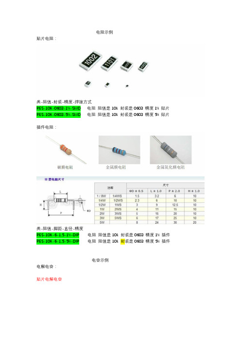
插件电阻规格尺寸
TVR-V压敏电阻中文资料
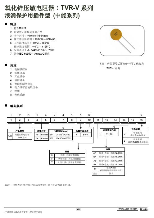
用途
1. 2. 3. 4. 5. 6. 7. 8. 电源供应器 家用电器 工业设备 通信设备 智能控制型电表 电力线智能通讯设备 照明 光伏系统
备注:产品型号后面打印一码 V 代表为 TVR-V 系列
编码规则
T 1 V 2 R 3 1 4 4 5 2 6 4 7 1 8 K 9 S 10 11 12 13 14 15
产品尺寸
35 39 42 49 53 58 65 70 80 85 92 92 95 98 100 110 130 140 155
适用于 SPD Type 3 应用
42
2013.03
产品规格与数据若有变更,恕不另行通知
氧化锌压敏电阻器:TVR-V 系列
浪涌保护用插件型 (中能系列)
(V) 340 360 395 455 500 550 595 650 710 775 845 930 1020 1120 1235 1355 1500 1650 1815
VDC
(V) 170 180 200 225 250 275 300 320 350 385 410 450 510 560 615 670 745 825 895
Cp
(pF) 970 880 820 720 650 600 550 500 440 400 370 340 300 290 270 250 220 200 180
UL rd 1449 3 SPD 应用类型*2
TVR14102-V 1000 (900~1100) TVR14112-V
1100 (990~1210)
备注:包装及内部控制代码未使用时, 第 11 码为可选后辍。
40
2013.03
产品规格与数据若有变更,恕不另行通知
插件国巨电阻规格书
Page-1Approval SheetforCarbon Film ResistorsCFR series±2% & ±5%YAGEO CORPORATIONHeadquarters: 3F, No.233-1, Pao Chiao Rd., Shin Tien, Taipei, Taiwan,R.O.C.Tel: 886-2-2917-7555 Fax: 886-2-2917-4286URL: Page-2Page-31. PRODUCT : CARBON FILM RESISTORS(Normal & Miniature Style)2. PART NUMBER : Part number of the carbon film resistor is identified by the name,power, tolerance, packing, temperature coefficient, special type and resistance value.Example :CFR -12 J T J 52 100RSeries Size Resistance Packing Temperature Special ResistanceName Code Tolerance Style Coefficient Type Value of Resistance(1) Style: CFR SERIES(2) Power Rating: -12=1/6W 、25S=1/4WS 、-25=1/4W 、50S=1/2WS 、-50=1/2W 、 1WS=1WS 、100=1W 、2WS=2WS 、200=2W(3) Tolerance: G=±2% J=±5%(4) Packaging Type : R =Paper Taping Reel T =Tape on Box Packing B =Bulk Packing(5) T .C .R : J=±350ppm/℃ — =lgnore(6) Special Type : 26=26mm 、52=52.4mm 、73=73mm 、 PN =PANAsert AV =AVlsert(7) Resistance Value: 1R 、10R 、100R 、10K 、100K 、330K 、1M………Page-43. BAND-CODE:4. ELECTRICAL CHARACTERISTICSTabe I*Standard resistance is 1Ω~ 10M Ω, below or over this resistance on request. *Rated Continuous Working Voltage (RCWV)=Value Resistance Rating Power ×FIG.1 TEMPERATURE COEFFICIENTPage-55. DERATING CURVE & HOT-SPOT TEMPERATURE6. DIMENSIONS7. ENVIRONMENTAL CHARACTERISTICS(1) Short Time Over Load TestAt 2.5 times of the rated voltage. (If the voltage exceeds the maximum load voltage, the maximum load voltage will be used as the rated voltage) applied for 5 seconds, the resistor should be free from defects after the resistor is released from load for about 30 minutes and the change of the resistance value should be within ±(0.25%+0.05Ω) as compared with the value before the test.Page-6(2) Dielectric Withstanding VoltageThe resistor is placed on the metal V Block. Apply a Table I dielectric withstanding between the terminals connected together with the block for about 60 seconds. The resistor shall be able to withstand without breakdown or flashover.(3) Temperature Coefficient TestTest of resistors above room temperature 125°C to 130°C (Testing Temperature) at the constant temperature silicon plate for over 4 to 5 minutes. Then measure the resistance. The Temperature Coefficient is calculated by the following equation and its value should be within the range of requested.600010t t 1R R R t Coefficien e Temperatur sistor Re ×−×−=R= Resistance value under the testing temperature R 0= Resistance value at the room temperature t = The testing temperature t o = Room temperature(4) Insulation ResistanceApply test terminal on lead and resistor body. The test resistance should be high than 10,000 Mohm.(5) SolderabilityImmerse the specimen into the solder pot at 230±5°C for 5±0.5 seconds. At least 95% solder coverage on the termination.(6) Resistance to SolventThe specimen into the appropriate solvent of Methyleme Chloride condition ofultrasonic machine for 1 minutes. The specimen is no deterioration of coatings and color code.(7) Terminal StrengthDirect Load – Resistors shall be held by one terminal and the load shall be gradually applied in the direction of the longitudinal axis of the resistor unit the applied load reacheds 5 pounds. The load shall be held for 10 seconds. The load of weight shall be ≧2.5kg(24.5N).Page-7(8) Pulse OverloadApply 4 times of rated voltage to the specimen at the 1 second on and 25 seconds off cycle, subjected to voltage application cycles specified in 10000. The change of the resistance value shall be within ±(2%+0.05Ω).(9) Load Life in HumidityPlace the specimen in a test chamber at 40±2°C and 90~95% relative humidity. Apply the rated voltage to the specimen at the 1.5 hours on and 0.5 hour off cycle. The total length of test is 1000 hours. The change of the resistance value shall be within ±(1.5%+0.05Ω).(10) Load Life TestPlaced in the constant temperature chamber of 70±3°C the resistor shall be connected to the lead wire at the point of 25mm. Length with each terminal, the resistors shall be arranged not much effected mutually by the temperature of the resistors and the excessive ventilation shall not be performed, for 90 minutes on and 30 minutes off under this condition the rated D.C. voltage is applied continuously for 1000+48/-0 hours then left at no-load for 1hour, the change of the resistance value measured at this time to the value before the test shall be within ±(1.5%+0.05Ω). There shall be no remarkable change in the appearance and the color code shall be legible after the test.(11) Temperature Cycling TestThe temperature cycle shown in the following table shall be repeated 5 times consecutively. The measurement of the resistance value is done before the first cycle and after ending the fifth cycle, leaving in the room temperature for about 1 hour, the change shall be within ±(1%+0.05Ω). After the test the resistor shall be free from the electrical or mechanical damage.Temperature Cycling Conditions: Step Temperature(°C) Time (minute)1 +25+10 -5 10 to152 -65+0 -3 30 3 +25+10 -5 10 to15 4+150+3 -030Page-8(12) Resistance to Soldering HeatThe terminal lead shall be dipped into the solder pot at 350±10°C for 3±0.5 seconds up to 3 mm. The change of the resistance value shall be within ±(1%+0.05Ω).8. PACKING METHODS Bandolier for Axial leadsThe resistors are supplied on bandolier, either 1000 resistors in ammopack or 5000 resistors on reel.9. TAPE ON REEL PACKING & TAPE ON BOX PACKING10. SPECIAL TYPE (FORMING DIMENSIONS)。
接插件标准
4.端子座及基座
• 材质:PBT(聚对苯二甲酸丁二醇酯 ) PA66 PA6(尼龙)
• 耐温: PBT、PA尼龙:-25~+85℃
• 耐燃烧: PA 94V-1、PBT 94V-2
• 绝缘阻抗: 500VDC 15S 20MΩ
5
5.端子与端子座装配间隙尺寸
• 公端子座与母端子座尺寸:0.10mm • 公端子座与母端子座锁扣间隙尺寸0.30~0.70mm • 端子与端子座窜动间隙尺寸:0.30~0.50mm • 端子与端子座孔四周间隙尺寸:0.05mm • 公端子插入对插件塑胶孔间隙,横向左右0.05mm,纵向上下0.05mm • 端子座及针座行间及列间距公差:0.05mm
2
2.端子抗弯性
材料厚度 最小弯曲力要求
≦0.20mm
4.0N
≦0.30mm
10.0N
≦0.40mm
15.0N
>0.40mm
20.0N
以上弯折角度30º,不可出现撕裂现象。
3
3.插针
• 厚度公差标准:0.02mm • 电镀膜厚标准: • a.镍底:20-40μ" • b.镀镍:70μ" • c.镀锡:80-120μ" • d.镀银:8-12μ" • e.镀金:1~3μ"(如有特殊要求另定) • 接触阻抗:20mΩ • 盐雾标准:24H、48H(好帮手用) • 材质:黄铜(H62)
2.8mm
6.35m m
*
20.0
10.0 5.0 1.5
不管什 么情况, 总连接 电阻不 得超过 20 mΩ
20MΩ
4.8KG
12
16.耐化学溶液能力试验
• 这个试验只是用于密封型连接 液体类型
插件电阻封装设计标准是什么

插件电阻封装设计标准是什么
插件电阻封装设计标准是指针对插件电阻的外观尺寸、结构、引脚布局、焊盘形状等进行规范和标准化的要求。
插件电阻是一种常用的电子元器件,用于限制电流、调整电路参数和实现分压等功能。
以下是常见的插件电阻封装设计标准:
1. 尺寸要求:插件电阻的尺寸应符合插入电路板的要求,一般采用直径和长度两个尺寸进行描述。
常见的直径尺寸有
2.5、
3.2、5.0、7.0等,长度尺寸一般为6.0、9.5、12.5、15.0等,
具体尺寸可根据实际需求确定。
2. 引脚布局:插件电阻的引脚布局应符合标准规定,在同一行或同一列上的引脚应间距均匀,并能够与插座或插针良好匹配,以确保插入稳固、可靠。
常见的引脚布局有单行直插、双行直插、倒插和多行直插等形式。
3. 引脚形状:插件电阻的引脚一般采用圆柱形状,直径和长度需要根据实际需求进行确定。
引脚的形状应保证插入电路板的稳固性和可靠性,一般采用弯脚、直脚、U形脚等形式。
4. 焊盘形状:插件电阻的焊盘形状应符合标准要求,以便于与焊盘或焊接点进行可靠连接。
常见的焊盘形状有圆形、方形、椭圆形等,需要根据实际焊接要求进行选择。
总之,插件电阻封装设计标准是根据实际应用需求和生产工艺要求来确定的,不同厂家和生产标准可能会有差异,因此在实际设计和选择过程中应参照相应的标准进行。
插件元器件引脚尺寸
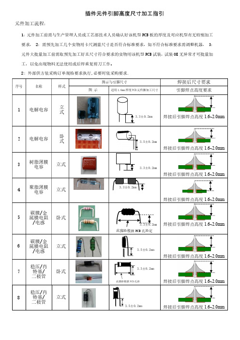
插件元件引脚高度尺寸加工指引
元件加工流程:
1:元件加工前需与生产管理人员或工艺部技术人员确认好该机型PCB板的厚度及对应机型有无特别加工要求, 2:需预先加工几个实物用卡尺测量尺寸是否符合标准要求,如不符合标准要求需调整机器, 3:元件大批量加工前需取预先加工好且尺寸符合要求的实物用该机型PCB试装,试装OK无异常才可批量加工,以免出现物料无法使用或后焊重复剪刀工作。
2: 外部供方依采购订单规格要求执行,必要时依采购要求.
焊接后引脚焊点高度1.6~2.0mm
焊接后引脚焊点高度1.6~2.0mm
焊接后引脚焊点高度1.6~2.0mm
焊接后引脚焊点高度1.6~2.0mm
焊接后引脚焊点高度1.6~2.0mm
3.5±0.2mm
焊接后引脚焊点高度1.6~2.0mm
此脚距根据PCB孔距焊接后引脚焊点高度1.6~2.0mm
焊接后引脚焊点高度1.6~2.0mm
焊接后引脚焊点高度1.6~2.0mm
焊接后引脚焊点高度1.6~2.0mm
焊接后引脚焊点高度1.6~2.0mm
焊接后引脚焊点高度1.6~2.0mm
焊接后引脚焊点高度1.8~2.4mm
焊接后引脚焊点高度1.6~2.0mm
焊接后引脚焊点高度1.6~2.0mm 3.3±0.2mm
焊接后引脚焊点高度1.8~2.4mm
焊接后引脚焊点高度1.6~2.0mm
焊接后引脚焊点高度1.6~2.0mm
焊接后引脚焊点高度2.0~2.4mm。
电子物料命名规则及图示(1)
说明:所有物料文件中含有其它物料时需要在该文件的第一行添加子类说明,严格按照相应子类添加到所属子类,没有该类则新建该子类。如:其它物料类-电池
二极管三极管 mos管 oled蜂鸣器蓝牙模块 电池 连接线 磁珠TVS管如何分类?
1.“二极管,三极管mos磁珠”建设为一个文档,分子标题管理,效果如图,建料号时分类严格建立
规格信息:器件名/型号/封装信息/(工作电压)
说明:二极管子类中包括普通二极管,双向二极管,tvs管
命名:
器件类型-型号-封装-焊接方式【中文备注信息电压,色光等】,中文备注信息没有的写无,如【无】。
如:
DIO-B5819WS-SOD323-SMD【40v】
二极管:DIO -型号:B5819WS-封装形式:SOD323-焊接方式:SMD【工作电压40v】
DIO-LED-0603-SMD【黄色】
二极管:DIO -类型:LED-封装形式:0603-焊接方式:SMD【黄色】
三极管:器件类型-型号-封装-焊接方式
AUD-9012-SOT23-SMD【无】
MOS管:器件类型-型号-封装-焊接方式
MOS-IRF7805Z-SO8-SMD【无】
TVS: 器件类型-型号-封装-焊接方式【电压】
TVS-SMCJ30A-SMC-SMD
2.OLED 等归入“显示屏幕”类,规格信息:名称-尺寸-引脚数-通信方式【备注颜色】
OLED -0.91寸-4pin-iic【黄色】
3.蜂鸣器列入“其它物料”类中,新建子类规格信息,格式:名称-尺寸-工作电压-焊接方式
buz-9*5.5-3v-DIP
4.蓝牙,WiFi等模块归入“模块物料”中,规格信息包括,型号,引脚数,品牌等
电子厂手工插件工艺标准
插装标准(4)
手工插件工艺标准—作业标准
• 组件 • 高压包完全插贴PCB,并且使卡扣完全卡入
PCB卡位 • 高频头完全插贴PCB,固定脚对角拧弯紧固,
与PCB相垂直 • 中频板、BBE板、图文板、立体声板等组
件,完全插贴PCB,并且使其与PCB相垂 直;直接插贴板面需点胶加固
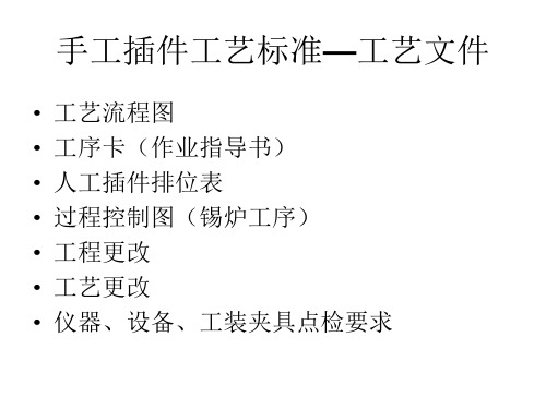
插装标准(5)
手工插件工艺标准—工艺文件
• 工艺流程图 • 工序卡(作业指导书) • 人工插件排位表 • 过程控制图(锡炉工序) • 工程更改 • 工艺更改 • 仪器、设备、工装夹具点检要求
手工插件工艺标准—作业标准
• 手指要尽量避免与元件引脚、PCB板焊盘 直接接触
• 大元件(如高压包)或PCB板组件拿取时, 应拿住能支撑整个元件(或组件)重量的 位置,而不能抓住象引线之类的脆弱部位
• 轻拿轻放
元器件拿取要求
手工插件工艺标准—作业准
• 元件成型应尽量使用专用的成型设备或夹 具。
• 元件成型标准:引脚长度相等且与PCB板 孔距一致;元件两端长度约1.5MM,引脚长度 一般为4~6MM
元件成型要求
手工插件工艺标准—作业标准
• 电阻 1/2W及以下功率电阻插平贴板面; 1W及以上功率电阻需预先成型,插件高度 即为成型高度。
手工插件工艺标准—作业标准
• 导线 线头<1MM,将导线和PCB的结合部用热 熔胶覆盖
• 其它如IC、变压器、开关、声表、插座等 元件均需插贴PCB
插装标准(6)
• 二极管 无磁环的二极管平贴PCB板插件 有磁环的二极管由磁环的高度决定 插装时需注意极性
插装标准(1)
手工插件工艺标准—作业标准
• 电容 • 磁介电容、绦纶电容、陶瓷滤波器自插料时
2w插件电阻的封装尺寸 -回复

2w插件电阻的封装尺寸-回复2W插件电阻的封装尺寸,或者说2瓦插件电阻的尺寸,是指一种电子元件,用于电路中的阻抗匹配、限流和分压等功能。
在设计和制造过程中,电子工程师需要了解这些电阻的封装尺寸以确保其安装和使用的可靠性。
本文将从封装类型、尺寸规格以及常见的应用场景等方面一步一步进行回答。
首先,我们来了解2W插件电阻的封装类型。
插件电阻分为多种类型,常见的有有线管型、无线管型和无线管型预折弯等。
其中,有线管型封装的插件电阻主要有两种标准尺寸,分别是9.0mm x 2.5mm和12.5mm x 3.5mm。
而无线管型封装的插件电阻则主要有3.2mm x 1.6mm、6.4mm x 3.2mm和8.0mm x 3.2mm等尺寸可供选择。
另外,无线管型预折弯封装的插件电阻一般有两种尺寸,分别为9.0mm x 3.5mm和12.5mm x 4.5mm。
接下来,我们将讨论2W插件电阻的尺寸规格。
2W插件电阻的尺寸规格主要包括长度、宽度和高度三个方面。
以9.0mm x 2.5mm封装的有线管型插件电阻为例,其长度通常为9.0mm,宽度为2.5mm,高度则根据电阻值和功率来确定。
同样地,以3.2mm x 1.6mm封装的无线管型插件电阻为例,其长度通常为3.2mm,宽度为1.6mm,高度也是根据电阻值和功率来确定。
总的来说,2W插件电阻的尺寸规格是有一定的可变性的,具体的尺寸可以根据不同的设计需求进行选择。
最后,我们来探讨2W插件电阻的应用场景。
2W插件电阻通常用于一些功率要求较高的电路中,如电源供应、稳压和限流电路等。
由于其具有较高的功率承受能力,插件电阻能够稳定地工作在高温和高电流的环境中。
此外,插件电阻的封装结构也使得其易于焊接和放置在电子电路板上。
因此,2W插件电阻在电子设备制造和维修中广泛应用。
总结起来,2W插件电阻的封装尺寸涉及到封装类型、尺寸规格和应用场景等方面。
不同类型的插件电阻有着不同的尺寸选项,且尺寸规格一般包括长度、宽度和高度。