CS2540 灯珠数码管驱动芯片
FM4115K LED恒流驱动IC说明书
FM4115K(文件编号:S&CIC1450)LED恒流驱动IC概述FM4115K是一款连续电感电流导通模式的降压恒流源,用于驱动一颗或多颗串联LED。
FM4115K输入电压范围从6伏到30伏,输出电流可调,最大可达1.2A。
根据不同的输入电压和外部器件,FM4115K可以驱动高达数十瓦的LED。
FM4115K内置功率开关,采用高端电流采样设置LED平均电流,并通过DIM引脚可以接受模拟调光和很宽范围的PWM调光。
当DIM的电压低于0.3伏时,功率开关关断,FM4115K进入极低工作电流的待机状态。
FM4115K采用SOT89-5封装和ESOP8封装。
特点极少的外部元器件;很宽的输入电压范围:从6V~30V;最大输出1.2A的电流(铝基板);复用DIM引脚进行LED开关、模拟调光和PWM调光;±3%的输出电流精度;LED开路自然保护;高达97%的效率;输出可调的恒流控制方法;增强散热能力的ESOP8封装可用于大功率驱动。
产品应用低压LED射灯代替卤素灯;车载LED灯;LED备用灯;LED信号灯。
TongshengtimesUseOnlyFM4115K (文件编号:S&CIC1450)LED 恒流驱动ICESOP-8功能模块图F o rT o ng s he n g t im e sFM4115K (文件编号:S&CIC1450)LED 恒流驱动IC参数特性注1:最大极限值是指超出该工作范围,芯片有可能损坏。
推荐工作范围是指在该范围内,器件功能正常,但并不完全保证满足个别性能指标。
电气参数定义了器件在工作范围内并且在保证特定性能指标的测试条件下的直流和交流电参数规范。
对于未给定上下限值的参数,该规范不予保证其精度,但其典型值合理反映了器件性能。
注2:温度升高最大功耗一定会减小,这也是由T JMAX ,θJA ,和环境温度T A 所决定的。
最大允许功耗为:P DMAX =(T JMAX -T A )/θJA 或是极限范围给出的数字中比较低的那个值。
CH455数码管驱动及键盘控制芯片说明书
数码管驱动及键盘控制芯片CH455中文手册版本:1E1、概述CH455是数码管显示驱动和键盘扫描控制芯片。
CH455内置时钟振荡电路,可以动态驱动4位数码管或者32只LED;同时还可以进行28键的键盘扫描;CH455通过SCL和SDA组成的2线串行接口与单片机等交换数据。
2、特点●内置显示电流驱动级,段电流不小于25mA,字电流不小于160mA。
●动态显示扫描控制,支持8×4或者7×4,直接驱动4位数码管或者32只发光管LED。
●内部限流,通过占空比设定提供8级亮度控制。
●内置28键键盘控制器,基于7×4矩阵键盘扫描。
●内置按键状态输入的下拉电阻,内置去抖动电路。
●提供低电平有效的键盘中断,提供按键释放标志位,可供查询按键按下与释放。
●高速2线串行接口,时钟速度从0到4MHz,兼容两线I2C总线,节约引脚。
●内置上电复位,支持2.7V~5V电源电压。
●支持低功耗睡眠,节约电能,可以被按键唤醒或者被命令操作唤醒。
●内置时钟振荡电路,不需要外部提供时钟或者外接振荡元器件,更抗干扰。
●提供DIP18、SOP18和SOP16三种无铅封装,兼容RoHS,功能和引脚部分兼容CH450芯片。
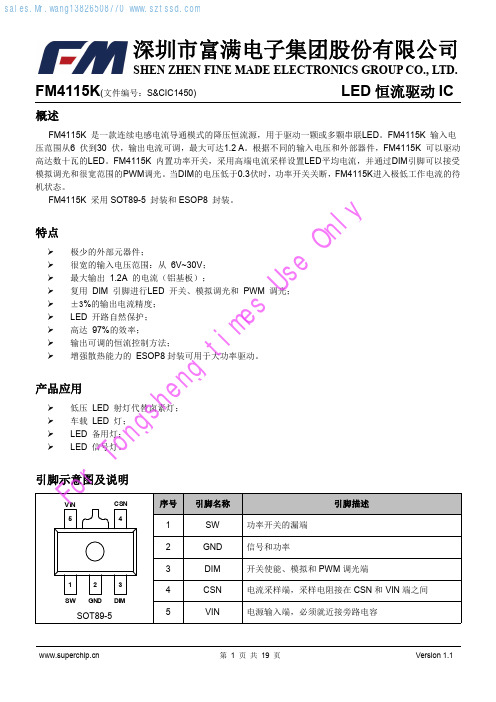
3、封装封装形式宽度引脚间距封装说明订货型号DIP18 7.62mm 300mil 2.54mm 100mil 标准18脚双列直插CH455K SOP18 7.62mm 300mil 1.27mm 50mil 标准的宽18脚贴片CH455H SOP16 3.9mm 150mil 1.27mm 50mil 标准的16脚贴片CH455G4、引脚引脚号引脚名称类型引脚说明DIP18/SOP18 SOP1611 14 VCC 电源正电源,持续电流不小于150mA4 8 GND 电源公共接地,持续电流不小于150mA9、10 12、13 14、15 16 12、1315、161、23SEG0~SEG6三态输出及输入数码管的段驱动,高电平有效,键盘扫描输入,高电平有效,内置下拉17 4 SEG7 输出数码管的小数点段驱动输出,高电平有效,7段模式下的键盘中断输出,低电平有效1、5 6、75、910、11DIG0~DIG3输出数码管的字驱动,低电平有效,键盘扫描输出,高电平有效3 7 SDA 内置上拉开漏输出及输入2线串行接口的数据输入和输出,内置上拉电阻2 6 SCL 输入2线串行接口的数据时钟,内置上拉电阻18 无INT# 内置上拉开漏输出键盘中断输出,低电平有效8 无ISET 输入段电流上限调整,悬空为默认设置5、功能说明5.1. 一般说明本手册中的数据,以B结尾的为二进制数,以H结尾的为十六进制数,否则为十进制数,标注为x的位表示该位可以是任意值。
深圳市凯斯得 LED 驱动 方案介绍
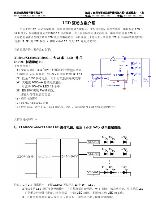
LED 驱动方案介绍市场上的LED 驱动方案较多,但总体趋势是要性能稳定,带恒流功能,转换效率高,串联驱动LED 灯10颗以上,驱动电流能力大的DC/DC 恒流模块,并且在实际中可以灵活应用,驱动串联,并联LED 灯。
上海芯龙最新研发的大功率LED 照明灯驱动芯片,可以涵盖几乎绝大部分的需要LED 恒流驱动的系统应用,(包括1W,3W 的LED 模组, N 多颗white LED 白光LED 阵列,背光等);目前已量产的主要产品有如下:XL6003/XL6004/XL6005----大功率LED 升压DC/DC 恒流驱动IC主要特点如下:(1)宽输入电压:3.6V~36V (低压可以兼顾锂电供电)(2)输出电压高:最高可升到42V ,可串联12颗1W LED(3)低至0.2V 参考电压,可以有效提高系统效率 (4)大电流1050mA 持续电流输出,可驱动1W~3W LED 12个串 (5)EN 脚可实现PWM 调光,且输入自带软启动功能(6)应用电路简单(7)SOP8L /TO252-5L 封装(8)应用领域:适用于基于LED 的汽车,路灯,太阳能灯及LED 背光驱动的应用。
具体应用列举如下:I :XL6003/XL6004/XL6005 LED 路灯电源,低压(小于36V )供电领域应用:特点:1.当24V 直流供电,单颗XL6003可以驱动12串1W LED 。
2.可以支持LED 路灯多路恒流输出,并且每路都具有恒流,PWM 调光,软启动功能,可以提高LED 灯的稳定性和使用寿命。
组合灵活,一路LED 故障,不影响其他LED 的工作。
3.升压应用领域对输入端的电压要求低,可以替代部分降压应用领域II :XL6003/XL6004/XL6005 太阳能LED 灯电源应用:0.5W~3W LED 灯太阳能LED 电源驱动方案60mW LED 阵列太阳能LED 电源驱动方案特点:1. XL6003/XL6004/XL6005是升压DC/DC 恒流驱动IC ,12V 蓄电池电压通过XL6003升压可以驱动12颗串联1W LED 灯。
LED显示屏原理详细解析(用到的芯片74HC138、74HC245、74HC595、4953、TB62726、JXI5020等芯片功能详解)
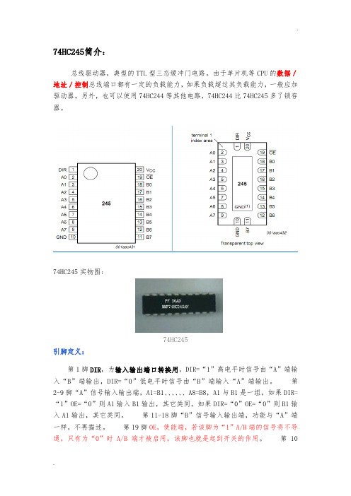
74HC245简介:总线驱动器,典型的TTL型三态缓冲门电路。
由于单片机等CPU的数据/地址/控制总线端口都有一定的负载能力,如果负载超过其负载能力,一般应加驱动器。
另外,也可以使用74HC244等其他电路,74HC244比74HC245多了锁存器。
74HC245实物图:74HC245引脚定义:第1脚DIR,为输入输出端口转换用,DIR=“1”高电平时信号由“A”端输入“B”端输出,DIR=“0”低电平时信号由“B”端输入“A”端输出。
第2-9脚“A”信号输入输出端,A1=B1、、、、、、A8=B8,A1与B1是一组,如果DIR=“1”OE=“0”则A1输入B1输出,其它类同。
如果DIR=“0”OE=“0”则B1输入A1输出,其它类同。
第11-18脚“B”信号输入输出端,功能与“A”端一样,不再描述。
第19脚OE,使能端,若该脚为“1”A/B端的信号将不导通,只有为“0”时A/B端才被启用,该脚也就是起到开关的作用。
第10脚GND,电源地。
第20脚VCC,电源正极。
TRUTH TABLE真值表Control Inputs 控制输入Operation 运行G DIRL L B 数据到A 总线L H A 数据到B 总线H X 隔开H=高电平 L=低电平×=不定Absolute Maximum Ratings绝对最大额定值Supply Voltage电源电压(VCC) -0.5 to -7.0V DC Input Voltage DIR and G pins (VIN) 直流输入电压方向和G引脚(输入电压)-1.5 to VCC -1.5V DC Input/Output Voltage (VIN, VOUT)直流输入/输出电压-0.5 to VCC -0.5V Clamp Diode Current 钳位二极管电流(ICD) ±20 mA DC Output Current直流输出电流,每个引脚(输出)±35 mA DC VCC or GND Current, per pin (ICC) ±70 mA Storage Temperature Range 储存温度范围(TSTG) -65℃ to -150℃Power Dissipation (PD)功耗(Note 3) 600 mW S.O. Package only 500 mW Lead Temperature (TL) (Soldering 10 seconds) 260℃【74HC245的作用:信号功率放大。
S4225开关调色温控制芯片

深圳市芯飞凌半导体有限公司
S4225xx 系列开关调色温控制芯片
AC
C1 :决定状态保持时间,一般 1uF 的电容
drv
可以保持 5S 左右
cs gnd
R1 1M R3 10 K (Vo max 13) / 5 R 2 (Vo min 13) / 1.5
其中: Vo max 是输出的最大电压 Vo min 是输出的最小电压
-----------------------------------------------------------------------------------------S4225XX-DS-V1p1 Page 9 of 9
深圳市芯飞凌半导体有限公司
S4225xx 系列开关调色温控制芯片
封装脚位图 管脚描述
管脚名 Vcc Vdd Clk Gnd D1,D2 IC供电脚 外接电容,实现保持时间 IC检测脚 信号和功率地 LED灯珠负极连接点 主要描述
图2 脚位图
订购信息
型号 S4225xS S4225xD 丝印 S4225xS 8EDxxx S4225xD 8EBxxx 包装形式 2500/盘,编带 2000/盒,管装
内置 400V1A 晶闸管,无需外挂开关管 外围原件简单,无需对 AC 输入检测 多个电源同时使用时无逻辑紊乱的问题 内置限压电路,保证可以更宽的工作范围 兼容隔离和非隔离的应用 专利技术,性能稳定
应用范围
设计提供便利性。
开关调色温的 LED 电源
典型应用
(其它请参考“外围参数计算”)
AC
典型应用其它请参考外围参数计算gndcsdrvacd2d1vccclkvddgndr2r1u1c1d1led1led2r3s42xxs4225典型图gndcsdrvacd2d1vccclkvddgndr2r1u1c1d1led1led2s42xx深圳市芯飞凌半导体有限公司s4225xx系列开关调色温控制芯片s4225xxdsv1p1wwwsdsemicompage脚位图订购信息型号丝印包装形式s4225xss4225xs8edxxx2500盘编带s4225xds4225xd8ebxxx2000盒管装note1l表示带小夜灯功能管脚描述管脚名主要描述vccic供电脚vdd外接电容实现保持时间clkic检测脚gnd信号和功率地d1d2led灯珠负极连接点应用极限参数note1参数范围vccgnd03v25vvddgnd03v6vclkgnd03v6vd1d2gnd03v55v工作温度范围
数码管_引脚图_驱动芯片

数码管的使用方法一、工作原理数码管是一种半导体发光器件,其基本单元是发光二极管。
能显示4位数字的叫四位数码管,当然也有多位和只有一位的数码管,他们的电气原理相同。
数码管按段数分为七段数码管和八段数码管,八段数码管比七段数码管多一个发光二极管单元(多一个小数点显示);按发光二极管单元连接方式分为共阳极数码管和共阴极数码管。
共阳数码管是指将所有发光二极管的阳极接到一起形成公共阳极(COM)的数码管。
共阳数码管在应用时应将公共极COM接到+5V,当某一字段发光二极管的阴极为低电平时,相应字段就点亮。
当某一字段的阴极为高电平时,相应字段就不亮。
共阴数码管是指将所有发光二极管的阴极接到一起形成公共阴极(COM)的数码管。
共阴数码管在应用时应将公共极COM接到地线GND上,当某一字段发光二极管的阳极为高电平时,相应字段就点亮。
当某一字段的阳极为低电平时,相应字段就不亮。
万联芯城-电子元器件采购网一直秉承着以良心做好良芯的服务理念,为广大客户提供一站式的电子元器件配单服务,客户行业涉及电子电工,智能工控,自动化,医疗安防等多个相关研发生产领域,所售电子元器件均为原厂渠道进货的原装现货库存。
只需提交BOM表,即可为您报价。
万联芯城同时为长电,顺络,先科ST等知名原厂的指定授权代理商,采购代理品牌电子元器件价格更有优势,欢迎广大客户咨询,点击进入万联芯城。
二、电气特性单位数码管有十个管脚,其中有8根是用来点亮a,b,c,d,e,f,dp 共8个发光二极管(原理中有介绍),3,8两个管脚为公共COM脚,它们相连通且作用相同,可接任意一根。
为了更清楚介绍,贴图如下:三、驱动方式静态驱动也称直流驱动。
静态驱动是指每个数码管的每一个段码都由一个单片机的I/O端口进行驱动,或者使用如BCD码二-十进制译码器译码进行驱动。
静态驱动的优点是编程简单,显示亮度高,缺点是占用I/O端口多,如驱动5个数码管静态显示则需要5×8=40根I/O端口来驱动,要知道一个89S51单片机可用的I/O端口才32个呢:),实际应用时必须增加译码驱动器进行驱动,增加了硬件电路的复杂性。
永嘉原厂VK1640B是LED数显驱动芯片,发光二极管显示驱动IC,8段12位共阴.12段8位共阳
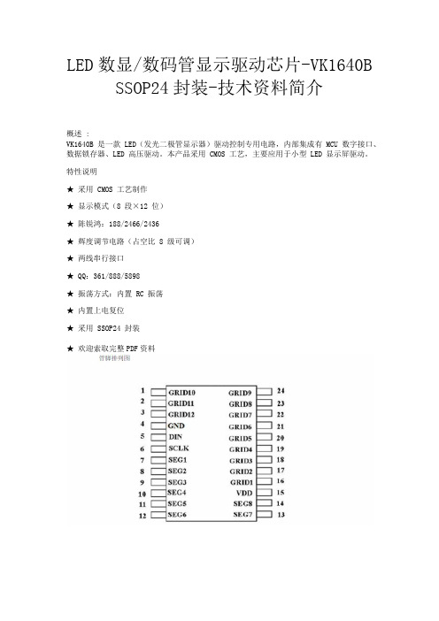
LED数显/数码管显示驱动芯片-VK1640B SSOP24封装-技术资料简介概述 :VK1640B 是一款 LED(发光二极管显示器)驱动控制专用电路,内部集成有 MCU 数字接口、数据锁存器、LED 高压驱动。
本产品采用 CMOS 工艺,主要应用于小型 LED 显示屏驱动。
特性说明★采用 CMOS 工艺制作★显示模式(8 段×12 位)★陈锐鸿:188/2466/2436★辉度调节电路(占空比 8 级可调)★两线串行接口★ QQ:361/888/5898★振荡方式:内置 RC 振荡★内置上电复位★采用 SSOP24 封装★欢迎索取完整PDF资料——————————————————————LCD/LED液晶控制器及驱动器系列芯片简介如下:RAM映射LCD控制器和驱动器系列:VK1024B 2.4~5.2V SEG*COM:6*4、6*3、6*2 偏置电压1/2 1/3 S0P-16VK1056B 2.4~5.2V SEG*COM:14*4、14*3/14*2偏置电压1/2 1/3 SOP/SSOP24 VK1072B 2.4~5.2V SEG*COM:18*4、18*3、18*2偏置电压1/2 1/3 SOP28VK1072C 2.4~5.2V SEG*COM:18*4、18*3、18*2偏置电压1/2 1/3 SOP28VK1072D 2.4~5.2V SEG*COM:18*4、18*3、18*2偏置电压1/2 1/3 SSOP28 VK1088B 2.4~5.2V SEG*COM:22*4、22*3、22*2 偏置电压1/2 1/3 QFN32(4*4) VK0192 2.4~5.2V 24seg*8com 偏置电压1/4 LQFP-44VK0256 2.4~5.2V 32seg*8com 偏置电压1/4 QFP-64VK0256B 2.4~5.2V 32seg*8com 偏置电压1/4 LQFP-64VK0256C 2.4~5.2V 32seg*8com 偏置电压1/4 LQFP-52VK1621 2.4~5.2V SEG*COM:32*4、32*3、32*2偏置电压1/2 1/3 LQFP44/48/SSOP48/SKY28/DICE裸片VK1622 2.4~5.5V 32seg*8com偏置电压1/4 LQFP44/48/52/64/QFP64/DICE裸片VK1623 2.4~5.2V 48seg*8com偏置电压1/4 LQFP-100/QFP-100/DICE裸片VK1625 2.4~5.2V 64seg*8com偏置电压1/4 LQFP-100/QFP-100/DICE 裸片VK1626 2.4~5.2V 48seg*16com偏置电压1/5 LQFP-100/QFP-100/DICE 裸片——————————————————————————————————高抗干扰LCD液晶控制器及驱动系列:VK2C21A 2.4~5.5V 20seg*4com 16*8 偏置电压1/3 1/4 I2C通讯接口 SOP-28VK2C21B 2.4~5.5V 16seg*4com 12*8 偏置电压1/3 1/4 I2C通讯接口 SOP-24VK2C21C 2.4~5.5V 12seg*4com 8*8 偏置电压1/3 1/4 I2C通讯接口 SOP-20VK2C21D 2.4~5.5V 8seg*4com 4*8 偏置电压1/3 1/4 I2C通讯接口 SOP-16VK2C22A 2.4~5.5V 44seg*4com 偏置电压1/2 1/3 I2C通讯接口 LQFP-52VK2C22B 2.4~5.5V 40seg*4com 偏置电压1/2 1/3 I2C通讯接口 LQFP-48VK2C23A 2.4~5.5V 56seg*4com 52*8 偏置电压1/3 1/4 I2C通讯接口 LQFP-64VK2C23B 2.4~5.5V 36seg*8com 偏置电压1/31/4 I2C通讯接口 LQFP-48VK2C24 2.4~5.5V 72seg*4com 68*8 60*16 偏置电压1/3 1/4 1/5 I2C通讯接口 LQFP-80超低功耗LCD液晶控制器及驱动系列:VKL060 2.5~5.5V 15seg*4com 偏置电压1/2 1/3 I2C通讯接口SSOP-24VKL128 2.5~5.5V 32seg*4com 偏置电压1/2 1/3 I2C通讯接口LQFP-44VKL144A 2.5~5.5V 36seg*4com 偏置电压1/2 1/3 I2C通讯接口TSSOP-48VKL144B 2.5~5.5V 36seg*4com 偏置电压1/21/3 I2C通讯接口QFN48L (6MM*6MM)静态显示LCD液晶控制器及驱动系列:VKS118 2.4~5.2V 118seg*2com 偏置电压 -- 4线通讯接口LQFP-128VKS232 2.4~5.2V 116seg*2com 偏置电压1/1 1/2 4线通讯接口LQFP-128内存映射的LED控制器及驱动器VK1628---通讯接口:STb/CLK/DIO 电源电压:5V(4.5~5.5V) 驱动点阵:70/52共阴驱动:10段7位/13段4位共阳驱动:7段10位按键:10x2 封装SOP28VK1629---通讯接口:STb/CLK/DIN/DOUT 电源电压:5V(4.5~5.5V) 驱动点阵:128共阴驱动:16段8位共阳驱动:8段16位按键:8x4 封装QFP44VK1629A---通讯接口:STb/CLK/DIO 电源电压:5V(4.5~5.5V) 驱动点阵:128共阴驱动:16段8位共阳驱动:8段16位按键:--- 封装SOP32VK1629B---通讯接口:STb/CLK/DIO 电源电压:5V(4.5~5.5V) 驱动点阵:112共阴驱动:14段8位共阳驱动:8段14位按键:8x2 封装SOP32VK1629C---通讯接口:STb/CLK/DIO 电源电压:5V(4.5~5.5V) 驱动点阵:120共阴驱动:15段8位共阳驱动:8段15位按键:8x1 封装SOP32VK1629D---通讯接口:STb/CLK/DIO 电源电压:5V(4.5~5.5V) 驱动点阵:96共阴驱动:12段8位共阳驱动:8段12位按键:8x4 封装SOP32VK1640---通讯接口: CLK/DIN 电源电压:5V(4.5~5.5V) 驱动点阵:128共阴驱动:8段16位共阳驱动:16段8位按键:--- 封装SOP28VK1640A---通讯接口: CLK/DIN 电源电压:5V(4.5~5.5V) 驱动点阵:128共阴驱动:8段16位共阳驱动:16段8位按键:--- 封装SSOP28VK1640B---通讯接口: CLK/DIN 电源电压:5V(4.5~5.5V) 驱动点阵:96 共阴驱动:8段12位共阳驱动:12段8位按键:--- 封装SSOP24VK1650---通讯接口: SCL/SDA 电源电压:5V(3.0~5.5V)共阴驱动:8段4位共阳驱动:4段8位按键:7x4 封装SOP16/DIP16VK1651---通讯接口: SCL/SDA 电源电压:5V(3.0~5.5V)共阴驱动:7段4位共阳驱动:4段7位按键:7x1 封装SOP16/DIP16VK1616---通讯接口: 三线串行电源电压:5V(3.0~5.5V)显示模式:7段4位按键:7x1 封装SOP16/DIP16VK1668---通讯接口:STb/CLK/DIO 电源电压:5V(4.5~5.5V) 驱动点阵:70/52共阴驱动:10段7位/13段4位共阳驱动:7段10位按键:10x2 封装SOP24VK6932---通讯接口:STb/CLK/DIN 电源电压:5V(4.5~5.5V) 驱动点阵:128共阴驱动:8段16位17.5/140mA 共阳驱动:16段8位按键:--- 封装SOP32VK16K33A/B/C---通讯接口:SCL/SDA 电源电压:5V(4.5V~5.5V)驱动点阵:128/96/64共阴驱动:16段8位/12段8位/8段8位共阳驱动:8段16位/8段12位/8段8位按键:13x3 10x3 8x3封装SOP20/SOP24/SOP28VK1618---带键盘扫描接口的LED驱动控制专用电路,内部集成有MCU数字接口、数据锁存器、键盘扫描等电路共阴驱动:5段7位/6段6位/7段5位/8段4位共阳驱动:7段5位/6段6位/5段7位/4段8位按键:5x1 封装SOP18/DIP18VK1S68C---LED驅動IC 10x7/13x4段位10段7位/11段6位共阴10x2按键,封装SSOP24VK1Q68D---LED驅動IC 10x7/13x4段位10段7位/11段6位共阴10x2按键,封装QFP24VK1S38A---LED驱动IC 8段×8位封装SSOP24VK1638--- LED驱动IC 共阴10段8位共阳8段10位封装SOP32——————————————————————————————————触摸触控IC系列简介如下:标准触控IC-电池供电系列:VKD223EB --- 工作电压/电流:2.0V-5.5V/5uA-3V 感应通道数:1 通讯接口最长响应时间快速模式60mS,低功耗模式220ms 封装:SOT23-6VKD223B --- 工作电压/电流:2.0V-5.5V/5uA-3V 感应通道数:1通讯接口最长响应时间快速模式60mS,低功耗模式220ms 封装:SOT23-6VKD233DB ---工作电压/电流:2.4V-5.5V/2.5uA-3V 1感应按键封装:SOT23-6 通讯接口:直接输出,锁存(toggle)输出低功耗模式电流2.5uA-3VVKD233DH ---工作电压/电流:2.4V-5.5V/2.5uA-3V 1感应按键封装:SOT23-6 通讯接口:直接输出,锁存(toggle)输出有效键最长时间检测16SVKD233DS ---工作电压/电流:2.4V-5.5V/2.5uA-3V 1感应按键封装:DFN6通讯接口:直接输出,锁存(toggle)输出低功耗模式电流2.5uA-3VVKD233DR ---工作电压/电流:2.4V-5.5V/1.5uA-3V 1感应按键封装:DFN6 通讯接口:直接输出,锁存(toggle)输出低功耗模式电流1.5uA-3VVKD233DG --- 工作电压/电流:2.4V-5.5V/2.5uA-3V 1感应按键封装:DFN6 通讯接口:直接输出,锁存(toggle)输出低功耗模式电流2.5uA-3VVKD233DQ --- 工作电压/电流:2.4V-5.5V/5uA-3V 1感应按键封装:SOT23-6通讯接口:直接输出,锁存(toggle)输出低功耗模式电流5uA-3VVKD233DM --- 工作电压/电流:2.4V-5.5V/5uA-3V 1感应按键封装:SOT23-6 (开漏输出)通讯接口:开漏输出,锁存(toggle)输出低功耗模式电流5uA-3VVKD232C--- 工作电压/电流:2.4V-5.5V/2.5uA-3V 感应通道数:2 封装:SOT23-6通讯接口:直接输出,低电平有效固定为多键输出模式,內建稳压电路——————————————————————————————————MTP触摸IC——VK36N系列抗电源辐射及手机干扰:VK3601L --- 工作电压/电流:2.4V-5.5V/4UA-3V3 感应通道数:1 1对1直接输出待机电流小,抗电源及手机干扰,可通过CAP调节灵敏封装:SOT23-6VK36N1D --- 工作电压/电流:2.2V-5.5V/7UA-3V3 感应通道数:1 1对1直接输出触摸积水仍可操作,抗电源及手机干扰,可通过CAP调节灵敏封装:SOT23-6VK36N2P --- 工作电压/电流:2.2V-5.5V/7UA-3V3 感应通道数:2 脉冲输出触摸积水仍可操作,抗电源及手机干扰,可通过CAP调节灵敏封装:SOT23-6VK3602XS ---工作电压/电流:2.4V-5.5V/60UA-3V 感应通道数:2 2对2锁存输出低功耗模式电流8uA-3V,抗电源辐射干扰,宽供电电压封装:SOP8VK3602K --- 工作电压/电流:2.4V-5.5V/60UA-3V 感应通道数:2 2对2直接输出低功耗模式电流8uA-3V,抗电源辐射干扰,宽供电电压封装:SOP8VK36N2D --- 工作电压/电流:2.2V-5.5V/7UA-3V3 感应通道数:2 1对1直接输出触摸积水仍可操作,抗电源及手机干扰,可通过CAP调节灵敏封装:SOP8VK36N3BT ---工作电压/电流:2.2V-5.5V/7UA-3V3 感应通道数:3 BCD码锁存输出触摸积水仍可操作,抗电源及手机干扰,可通过CAP调节灵敏封装:SOP8VK36N3BD ---工作电压/电流:2.2V-5.5V/7UA-3V3 感应通道数:3 BCD码直接输出触摸积水仍可操作,抗电源及手机干扰,可通过CAP调节灵敏封装:SOP8VK36N3BO ---工作电压/电流:2.2V-5.5V/7UA-3V3 感应通道数:3 BCD码开漏输出触摸积水仍可操作,抗电源及手机干扰封装:SOP8/DFN8(超小超薄体积)VK36N3D --- 工作电压/电流:2.2V-5.5V/7UA-3V3 感应通道数:3 1对1直接输出触摸积水仍可操作,抗电源及手机干扰封装:SOP16/DFN16(超小超薄体积)VK36N4B ---工作电压/电流:2.2V-5.5V/7UA-3V3 感应通道数:4 BCD输出触摸积水仍可操作,抗电源及手机干扰封装:SOP16/DFN16(超小超薄体积)VK36N4I---工作电压/电流:2.2V-5.5V/7UA-3V3 感应通道数:4 I2C输出触摸积水仍可操作,抗电源及手机干扰封装:SOP16/DFN16(超小超薄体积)VK36N5D ---工作电压/电流:2.2V-5.5V/7UA-3V3 感应通道数:5 1对1直接输出触摸积水仍可操作,抗电源及手机干扰封装:SOP16/DFN16(超小超薄体积)VK36N5B ---工作电压/电流:2.2V-5.5V/7UA-3V3 感应通道数:5 BCD输出触摸积水仍可操作,抗电源及手机干扰封装:SOP16/DFN16(超小超薄体积)VK36N5I ---工作电压/电流:2.2V-5.5V/7UA-3V3 感应通道数:5 I2C输出触摸积水仍可操作,抗电源及手机干扰封装:SOP16/DFN16(超小超薄体积)VK36N6D --- 工作电压/电流:2.2V-5.5V/7UA-3V3 感应通道数:6 1对1直接输出触摸积水仍可操作,抗电源及手机干扰封装:SOP16/DFN16(超小超薄体积)VK36N6B ---工作电压/电流:2.2V-5.5V/7UA-3V3 感应通道数:6 BCD输出触摸积水仍可操作,抗电源及手机干扰封装:SOP16/DFN16(超小超薄体积)VK36N6I ---工作电压/电流:2.2V-5.5V/7UA-3V3 感应通道数:6 I2C输出触摸积水仍可操作,抗电源及手机干扰封装:SOP16/DFN16(超小超薄体积)VK36N7B ---工作电压/电流:2.2V-5.5V/7UA-3V3 感应通道数:7 BCD输出触摸积水仍可操作,抗电源及手机干扰封装:SOP16/DFN16(超小超薄体积)VK36N7I ---工作电压/电流:2.2V-5.5V/7UA-3V3 感应通道数:7 I2C输出触摸积水仍可操作,抗电源及手机干扰封装:SOP16/DFN16(超小超薄体积)VK36N8B ---工作电压/电流:2.2V-5.5V/7UA-3V3 感应通道数:8 BCD输出触摸积水仍可操作,抗电源及手机干扰封装:SOP16/DFN16(超小超薄体积)VK36N8I ---工作电压/电流:2.2V-5.5V/7UA-3V3 感应通道数:8 I2C输出触摸积水仍可操作,抗电源及手机干扰封装:SOP16/DFN16(超小超薄体积)VK36N9I ---工作电压/电流:2.2V-5.5V/7UA-3V3 感应通道数:9 I2C输出触摸积水仍可操作,抗电源及手机干扰封装:SOP16/DFN16(超小超薄体积)VK36N10I ---工作电压/电流:2.2V-5.5V/7UA-3V3 感应通道数:10 I2C输出触摸积水仍可操作,抗电源及手机干扰封装:SOP16/DFN16(超小超薄体积)——————————————————————————————————1-8点高灵敏度液体水位检测IC——VK36W系列VK36W1D ---工作电压/电流:2.2V-5.5V/10UA-3V3 1对1直接输出水位检测通道:1可用于不同壁厚和不同水质水位检测,抗电源/手机干扰封装:SOT23-6备注:1. 开漏输出低电平有效2、适合需要抗干扰性好的产品应用VK36W2D ---工作电压/电流:2.2V-5.5V/10UA-3V3 1对1直接输出水位检测通道:2可用于不同壁厚和不同水质水位检测,抗电源/手机干扰封装:SOP8备注:1. 1对1直接输出 2、输出模式/输出电平可通过IO选择VK36W4D ---工作电压/电流:2.2V-5.5V/10UA-3V3 1对1直接输出水位检测通道:4可用于不同壁厚和不同水质水位检测,抗电源/手机干扰封装:SOP16/DFN16 备注:1. 1对1直接输出 2、输出模式/输出电平可通过IO选择VK36W6D ---工作电压/电流:2.2V-5.5V/10UA-3V3 1对1直接输出水位检测通道:6可用于不同壁厚和不同水质水位检测,抗电源/手机干扰封装:SOP16/DFN16 备注:1. 1对1直接输出2、输出模式/输出电平可通过IO选择VK36W8I ---工作电压/电流:2.2V-5.5V/10UA-3V3 I2C输出水位检测通道:8可用于不同壁厚和不同水质水位检测,抗电源/手机干扰封装:SOP16/DFN16。
奥斯特里亚米科斯AS2540 CMOS集成电路说明书
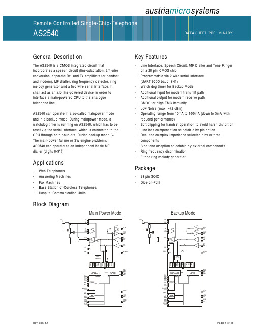
Data Sheet AS2540austria micro systemsaustria micro systemsGeneral DescriptionThe AS2540 is a CMOS integrated circuit that incorporates a speech circuit (line-adaptation, 2/4-wire conversion, separate Rx- and Tx-amplifiers for handset and modem), MF dialler, ring frequency detector, ring melody generator and a two wire serial interface. It shall act as an a/b-line-powered device in order to interface a main-powered CPU to the analogue telephone line.AS2540 can operate in a so-called mainpower mode and in a backup mode. During mainpower mode, a watchdog timer is running on AS2540, which has to be reset via the serial interface, which is connected to the CPU through opto-couplers. During backup mode (= The main-power failure or SW engine problem),AS2540 can operate as an independent basic MF dialler (digits 0-9*#)Applications-Web Telephones-Answering Machines-Fax Machines-Base Station of Cordless Telephones-Hospital Communication Units Key Features-Line Interface, Speech Circuit, MF Dialler and Tone Ringer on a 28 pin CMOS chip-Programmable via 2-wire serial interface(UART 9600 baud, 8N1)-Watch dog timer for Backup Mode-Additional input for modem transmit path-Additional output for modem receive path-CMOS for high EMC immunity-Low Noise (max. –72 dBm)-Operating range from 15mA to 100mA (down to 5mA with reduced performance)-Soft clipping for handset operation to avoid harsh distortion -Line loss compensation selectable by pin option-Real and complex impedance selectable by external components-Side tone adaption selectable by external components-Ring frequency discrimination-3-tone ring melody generatorPackage-28 pin SOIC-Dice-on-FoilBlock DiagramMain Power Mode Backup ModePin Description15RFD R ing F requency D iscriminationSchmitt trigger input for ring frequency discrimination. Disabled during off-hook.7LS L ine Current S ense InputInput for sensing the line current5LI L ine I nputInput used for power extraction and line current sensing6RI R eceive I nputInput for ac-separated receive signal2STB S ide T one B alance InputInput for side tone cancellation network3CS C urrent S hunt Control OutputN-channel open drain output to control the external high power shunt transistor for synthesising ac- anddc- impedance, modulation of line voltage and shorting the line during make periods of pulse dialling8CI C omplex I mpedance InputInput pin for the capacitor to program a complex impedance16DPn D ial P ulse OutputOpen drain output pulls low during break periods of pulse dialling and flash17EHS E lectronic H ook S witchSchmitt Trigger Input to detect an electronic off-hook.18MHS M anual H ook S witchSchmitt Trigger Input to detect a manual off-hook.19MODE D TMF L evel S election-4/-6dBm—>DLS open-6/-8dBm—>DLS-r1-8/-10dBm—>DLS-r2L ine L oss C ompensation Select Pin45mA-75mA—>LLC open20mA-50mA—>LLC-r3None—>LLC-r428MO Ring M elody O utputPDM output of the ring melody generator.11VDD V oltage D rain D rainPositive Power Supply4VSS V oltage S ource S ourceNegative Power Supply25OSC O scillator InputInput for ceramic resonator 3.58MHz.Recommended type: Murata CSA 3.58MG312AM or compatible12AGND A nalogue G roundSpecial ground for the internal amplifiers26RXD R eceive D ata InputSchmitt trigger input to serial interface27TXD T ransmit D ata OutputOpen drain output from serial interface20 21R1R2Keyboard R ows22 23 24C1C2C3Keyboard C olumns10ROT R eceive O utput to T ransformerOutput for driving a transformer with an ac impedance larger than 10kΩ1TIT T ransformer I nput from T ransformerSingle ended input for transformer9ROH R eceive O utput to H andsetOutput for driving a dynamic earpiece with an impedance from 150Ω to 300Ω13 14M2M1M icrophone InputsDifferential inputs for the microphone (electret)Functional DescriptionModes of operationThere are 4 possible modes:Idle ModeManual hook-switch and electronic hook-switch (e.g. relay) is open (MHS ∩ EHS = logical 0), no ring signal is applied, the oscillator is stopped, signalling via the serial interface is not possible.Ringing ModeAS2540 is supplied via the ring capacitor and external path, manual hook -switch and electronic hook-switch is open (MHS ∩ EHS = logical 0), the oscillator is running, a valid incoming ringing is signalled via the serial interface to the CPU. If the CPU does not reply the AS2540 switches into backup mode and sends a ring melody to the MO output.Backup ModeManual hook-switch and/or electronic hook-switch is closed (MHS ∪ EHS = logical 1), AS2540 is supplied with line current, the oscillator is running, the keyscan is enabled and the handset path is switched on, signalling via the serial interface is possible. After AS2540 has started dialling in backup mode, he must not be interrupted any more in order to ensure consistent dialling. A mode transition BM -> MPM is only possible before AS2540 has started dialling digits independently.Main Power ModeManual hook-switch and/or electronic hook-switch is closed, AS2540 is supplied with line current (MHS ∪ EHS = logical 1), the oscillator is running, the keyscan is disabled, AS2540 is controlled via the serial interface, handset path or monitor path or modem path is on, signalling via the serial interface is possible.Select Operation Mode<SetHandsetPath>SROH SROT & STIT <SetModemPath>SROT & STIT<SetMonitorPath>SROH & SROT STIT Example Main Power ModeStart-up in backup modeAs soon as AS2540 is supplied with line current, the external V dd capacitor will be charged up via the LI and VDD pin and after the V dd voltage has reached the operating level, the handset path of the speech circuit is switched on. This off-hook status is also signalled to the internal logic via the MHS or EHS pin in order to start the pinscan and subsequently set the country specific modes. Additionally a <LineEvent> message is sent to the CPU.Start-up in ring modeWhen a ringing signal is applied to the line, V dd of AS2540 is charged up via an external path. After V dd has reached the operating voltage the oscillator starts and AS2540 discriminates the ring frequency. After a valid ring frequency is applied on the RFD pin, the logic sends a<LineEvent> message is sent to the CPU and a watchdog timer is started. When the <LineEvent> message is not quit by the CPU before the watchdog timer has finished the countdown, AS2540 changes into backup mode and sends out a melody via the MO pin.DC conditionsThe normal operating mode is from 15mA to 100mA. An operating mode with reduced performance is from 5mA to 15mA. In the line hold range from 0mA to 5mA the device is in a power down mode and the voltage at LI is reduced to a maximum of 3.5VReceive pathThe gain of the LS —> ROH receive path is set to 2dB for ac-impedance 1000Ω. The receive input is the differentialsignal of RI and STB. During DTMF dialling a MF comfort tone is applied to ROH which is -30dB relative to the line level. The soft clip circuit limits the output voltage at ROH to 1V p. It prevents harsh distortion and acoustic shock.The gain of the LS —> ROT receive path is set to 0dB for ac-impedance 1000Ω. The receive input is the differential signal of RI and STB. The soft clip circuit is not active for this output.ModescanThe DTMF-level on the line and the function of the line loss compensation can be selected with the connection of the MODE-pin to the keyboard matrix. The MODE-pin is scanned once after each OFF-Hook transition.C3C2C1R2R1LLC Dtmf Level 45mA-75mA -6dBm XX45mA-75mA -8dBm X45mA-75mA -10dBm X20mA-50mA -6dBm X20mA-50mA-8dBm X X 20mA-50mA -10dBm XXNo LLC -6dBm X X No LLC -8dBm XXX No LLC-10dBmX indicates connection to pin modeSerial interfaceThe communication principle is derived from a standard UART: -Baud Rate9600-Start Bit1-Data Bits8-Parity None-Stop Bit1-LSB is transferred prior to MSBRx - messagesX MSB X d5d4d3d2d11LSBx x010101Digit 0Starts DTMF dialling of digit x x000011Digit 1Starts DTMF dialling of digit x x000101Digit 2Starts DTMF dialling of digit x x000111Digit 3Starts DTMF dialling of digit x x001001Digit 4Starts DTMF dialling of digit x x001011Digit 5Starts DTMF dialling of digit x x001101Digit 6Starts DTMF dialling of digit x x001111Digit 7Starts DTMF dialling of digit x x010001Digit 8Starts DTMF dialling of digit x x010011Digit 9Starts DTMF dialling of digit x x010111Digit *Starts DTMF dialling of digit x x000001Digit #Starts DTMF dialling of digit x x011001Digit A Starts DTMF dialling of digit x x011011Digit B Starts DTMF dialling of digit x x011101Digit C Starts DTMF dialling of digit x x011111Digit D Starts DTMF dialling of digit x x100001KeyReleased Stops Diallingx x101101SetDPn_HIGH Release pin Dpn (open drain) x x100011SetDPn_LOW Force pin DPn = VSSx x100101SetMask Force LI-Voltage to 1.2 Vx x100111ResetMaskx x101111SetTestmode FOR FACTORY TEST ONLY x x101001MuteON Mute Transmit pathx x101011MuteOFFx x110011SetHandsetPathx x111011SetMonitorPathx x110101SetModemPathx x110001RequestStatus AS2540 sends Status information x x110111reserved<LineEvent>x x111001reserved<LineEvent>x x111101reserved<LineEvent>x x111111reserved<LineEvent>Tx messages<Ack> messageb7 MSB b6b5b4b3b201LSB7643101valid ring signal detected001no ring signal101manual hook switch - off-hook (pin MHS)001manual hook switch - on-hook (pin MHS)101electronic hook switch - off-hook (pin EHS)001electronic hook switch - on-hook (pin EHS)Status of AS254000001no LLC comparator .....................00101LLC comparator 20mA (45mA) ...01001LLC comparator 26mA (51mA) ...01101LLC comparator 32mA (57mA) ... 10001LLC comparator 38mA (63mA) ... 10101LLC comparator 44mA (69mA) ... 11001LLC comparator 50mA (75mA) ...coded status of LLC comparator<Line Event> Messageb7 MSB b6b511111LSB76431111101valid ring signal detected0111101no ring signal1111101manual hook switch - off-hook (pin MHS)0111101manual hook switch - on-hook (pin MHS)1111101electronic hook switch - off-hook (pin EHS)0111101electronic hook switch - on-hook (pin EHS)Status of AS2540 ProtocolLine EventsAS2540 has 3 inputs, namely MHS (Manual Hook Switch), EHS (Electronic Hook Switch) and RFD (Ring Frequency Detector), which sense the state of the two hook-switches and discriminate an applied ring signal. The MHS is connected to the manual hook switch which is operated by the handset and the EHS is connected to an electronic hook switch which is operated by the CPU. Whenever the state of these inputs changes, AS2540 immediately sends <LineEvent> to the CPU after a debounce time. MHS and EHS up-debouncing lasts 15ms, down-debouncing lasts 85ms. RFD start to discriminate the ring frequency immediately but will send a <LineEvent> message with a delay of 102ms. A status change of MHS and EHS pins must not change the momentary selected path of the speech network.The <LineEvent>-message is sent without consideration of the momentary activities of AS2540 in order to meet PTT requirements (e.g. line break signalling). The code for the <LineEvent>-message is chosen with regard to the minimum current consumption in order to operate the optocouplers. Pending <Ack>-messages will be queued after the <LineEvent>-message. An already running transmissions of <Ack> will not be interrupted and<LineEvent> will be sent afterwards in this case.-Mode transitions Idle → BM → MPM → Idle AS2540 always starts up in backup mode and is prepared to act like an independent dialler. <LineEvent> is sent to the CPU and AS2540 remains in back-up mode until any valid message is sent from the CPU. This makes sure that a non-operable CPU does not disable basic dialling functions.-Mode transition MPM → BMA watchdog timer is started after <LineEvent> and is reset whenever AS2540 receives a message from the CPU via the serial interface. If the CPU does not send any further valid message within 2400ms, AS2540 goes back into back-up mode, immediately locks the UART and remains in backup mode till next on-hook.Dialling FunctionsDTMFThe DTMF generator provides 8 frequencies (in Hz):11697+120922697+133633697+147744770+120955770+133666770+147777852+120988852+133699852+1477*941+120900941+1336#941+1477The MF output levels are set to -4/-6dB which should allowefficient backup dialling under all line conditions. The TONE/PAUSE ratio is 90ms/90ms. The preemphasis between low group and high group frequencies is t.m.2.6dB.FLASH timingCPU can control the DPn pin and the MASK-mode ofAS2540 via serial interface.Tone RingerRing frequency discriminationThe ring frequency discrimination assures that only signals with a frequency between 13Hz and 70Hz are regarded as valid ring signals.When a valid ring signal is present for 102ms continuously, the ring melody generator is activated and remains active as long as a valid ring signal is present.Once the ring melody generator has started, the ring signal is continuously monitored and the ring melody generator is instantly turned off according to the momentary presence of a valid or invalid ring signal until next off-hook.Toner ringer melodyThe 3 basic melody frequencies are:-F1=880Hz-F2=1067Hz-F3=1333HzThe repetition rate is set to 4 which means that the sequence of F1, F2, F3, F1, F2, F3 is repeated 4 times within a second.Keyboard connectionsDouble contacts under keys 0-9*#: One contact is connected to AS2540, the other one to CPU.Electrical characteristicsElectrical characteristics are measured with the Test Circuit application. Typical mean values will not be tested.Absolute maximum ratingsPositive Supply Voltage-0.3V <= V DD <= 7V Input Current+/- 25mA Input Voltage (LS)-0.3V <= V in <= 10V Input Voltage (LI, CS)-0.3V <= V in <= 8V Input Voltage (STB, RI)-2V <= V in <= V DD+0.3V Digital Input Voltage-0.3V <= V in <= V DD+0.3V Electrostatic Discharge (HBM 1.5kΩ-100pF)+/- 800V Storage Temperature-65°C to +125°CRecommended operating conditionsSupply Voltage (generated internally) 3.6V <= V DD <= 5VOscillator FrequencyResonator Murata CSA 3.58MG312AM 3.58MHz Operating Temperature-15°C to +60°CDC characteristicsI Line=15mA w/o operation of SI through optocouplers, unless other specifiedI DD Operating Current Speech ModeSpeech Mode with SIMF DiallingLD Dialling, V DD=2.5VRing Mode, V DD=2.5V3542003005mAmAmAµAµAYNNNNV LI Line Voltage15mA<=I LINE<=100mA 4.2 4.5 4.8V Y I OL Output Current, Sink CS,DPn, MO TXD V OL=0.4VV OL=10mA110mAmANNI OH Output Current, Source MOV OH=V DD-0.4V-1mA NTransmit characteristicsA MTX Transmit GainM1/M2 —> LSZ AC(syn)=1000Ω+36.5+38+39.5dB YA TTX Transmit GainTIT —> LSZ AC(syn)=1000Ω+6.5+8+9.5dB Y THD Distortion V LS=0.25V RMS2%Y V AGC Soft Clip LevelM1/M2 —> LS at LS2.0V P NA SCO Soft Clip OverdriveM1/M220dB NZ IN Input ImpedanceM1/M2 - TIT20kΩNV NO Noise Output VoltageLST AMP=25°C-72dBmp Y RL Return Loss Z AC(syn)=1000Ω18dB Y Receive characteristicsA HRX Receive GainLS —> ROHZ AC(syn)=1000Ω+0.5+2+3.5dB YA TRX Receive GainLS —> ROT Z AC(syn)=1000Ω-3.5-2-0.5dB YYTHD Distortion V LS=0.25V RMS2%YV AGC Soft Clip LevelROH1V P NA SCO Soft Clip OverdriveROH10dB NV NO Noise Output VoltageROH - ROTT AMP=25°C-72dBmp Y Z IN Input Imp. RI8kΩN ST Sidetone V RI<=0.25V RMS24dB Y RL Return Loss Z AC(syn)=1000Ω18dB YLD characteristicst(td)Flash Duration DPN pin status can be directlycontrolled via serial interfaceDTMF characteristicsV MFlow Tone Level Low GroupLS-6dBm Y ∆V L-H Preemphasis L-H 2.0 2.6 3.2dB YUFC Unwanted FrequencyComponents 300Hz - 4.3kHz4.3kHz - 7kHz7kHz - 10kHz10kHz - 14kHz14kHz - 28.5kHz28.5kHz – 40kHz-40-46-52-58-70-80dBmdBmdBmdBmdBmdBmYYYYYY∆f Frequency Deviation 1.2%Y t(td)Tone Duration8082.385ms Y t(itp)Inter Tone Pause8082.385ms Y t(mo)Mute Overhang6ms Y V CT-H Comfort Tone (DTMF)ROH rel. to LS-30dB NRinger characteristicsf1Frequency 1770800830Hz Y f2Frequency 2102510671110Hz Y f3Frequency 3128013331385Hz Y f MIN Min. Det. Frequency121314Hz Y f MAX Max. Det. Frequency687075Hz Y t DT Detection Time Initially102ms NSerial Interfacet RXD-r RXD signal rise time V dd=4V,R Pull-up=1.2kΩ30µs N t RXD-f RXD signal fall time30µs NV dd/2V N V comp Input comparator level atRXDBR RXD RXD baud rate+/-2%9600bps N BR TXD TXD baud rate+/-2%9600bps YMiscellaneoust D Key Debouce Time15ms N t time-out Watch-dog Timer2400ms NTypical ApplicationTest CircuitILine28-pin plastic SOIC (suffix T)Max. Body Length18.1mm / 713milMax. Body Width7.6mm / 300milPitch 1.27mm / 50milPin-out1–TIT–28 2–STB–27 3–CS–26 4–VSS–25 5–LI–24 6–RI–23 7–LS–22 8–CI–21 9–ROH–20 10–ROT–19 11–VDD–18 12–AGD–17 13–M1–16 14–M2–15MarkingYYWWAAA Ordering InformationNumber Package DescriptionAS2540T SOIC28plastic small outline package -28 leads (suffix T)AS2540Q Dice-on-Foil diceDevices sold by austriamicrosystems AG are covered bythe warranty and patent identification provisions appearingin its Term of Sale. austriamicrosystems AG makes no warranty, express, statutory, implied, or by description regarding the information set forth herein or regarding the freedom of the described devices from patent infringement. austriamicrosystems AG reserves the right to change specifications and prices at any time and without notice. Therefore, prior to designing this product into a system, itis necessary to check with austriamicrosystems AG for current information. This product is intended for use in normal commercial applications. Applications requiring extended temperature range, unusual environmental requirements, or high reliability applications, such as military, medical life-support or life-sustaining equipmentare specifically not recommended without additional processing by austriamicrosystems AG for each application.CopyrightCopyright © 1997-2002, austriamicrosystems AG, Schloss Premstaetten, 8141 Unterpremstaetten, Austria-Europe. Trademarks Registered ®. All rights reserved. The material herein may not be reproduced, adapted, merged, translated, stored, or used without the prior written consentof the copyright owner.The information furnished here by austriamicrosystems AGis believed to be correct and accurate. However, austriamicrosystems AG shall not be liable to recipient or any third party for any damages, including but not limitedto personal injury, property damage, loss of profits, loss of use, interruption of business or indirect, special, incidentalor consequential damages, of any kind, in connection withor arising out of the furnishing, performance or use of the technical data herein. No obligation or liability to recipientor any third party shall arise or flow out of austriamicrosystems AG rendering of technical or other services.USA (east)austriamicrosystems USA, Inc.Suite 400, 8601 Six Forks RoadRaleigh, NC 27615, USAPhone: +1/919/676 5292Fax: +1/919/676 5305United Kingdomaustriamicrosystems UK, Ltd.Coliseum Business Centre, Watchmoor Park Camberley, Surrey, GU15 3YL, UKPhone: +44/1276/23 3 99Fax: +44/1276/29 3 53Japanaustriamicrosystems AGShin Yokohama Daini, Center Bldg. 10F3-19-5, Shin YokohamaKohoku-ku, Yokohama 222-0033, JapanPhone: +81/45/474 0962Fax: +81/45/472 9845Distributors & Representatives austriamicrosystems AG is represented by distributors in the following countries. Please contact your nearest regional sales office for the distributor address: Spain, Israel, Korea, Hong-Kong, Taiwan, Malaysia, Singapore, India, BrazilApplication SupportPlease contact your local sales office or your distributor.。
- 1、下载文档前请自行甄别文档内容的完整性,平台不提供额外的编辑、内容补充、找答案等附加服务。
- 2、"仅部分预览"的文档,不可在线预览部分如存在完整性等问题,可反馈申请退款(可完整预览的文档不适用该条件!)。
- 3、如文档侵犯您的权益,请联系客服反馈,我们会尽快为您处理(人工客服工作时间:9:00-18:30)。
IUP2
SDA引腳的輸入(或輸出)上拉電流
IUP3
ADDR或 STB引腳的輸入上拉電流
VR
上電重定的預設電壓門限
最小值 3.0
-0.5 2.0 4.2 4.5 -5
2.3
典型值 5 80
最大值 6.0 120 0.1 0.8
VCC+0.5 0.8
0.5
0
5
250
400
3
200
2.6
2.8
單位 V mA mA V V V V V V uA uA uA V
空
引腳說明 正電源,持續電流不小於 120mA 公共接地,持續電流不小於 120mA
段驅動輸出 字驅動輸出 序列介面的時鐘輸入 序列介面的資料登錄 保留引腳,禁止連接
空腳
微處理器的資料通過兩線匯流排介面和CS2540通信,在輸入資料時當SCLK 是高電平時, DIN 上的信號必須保持不變;只有SCLK上的時鐘信號為低電平時,DIN上的信號才能改變。資 料的輸入總是低位元元在前,高位在後傳輸.資料登錄的開始條件是CLK 為高電平時,DIN 由高變 低;結束條件是SCLK為高時,DIN由低電平變為高電平。 指令資料傳輸過程如下圖:
內部時序參數(測試條件:TA=25℃,VCC=5V)
(注:本表時序參數都是內置時鐘週期的倍數,內置時鐘的頻率隨著電源電壓的降低而降低)
名稱
參數說明
最小值
典型值
最大值
單位
TPR
電源上電檢測產Th的復位時間
5
8
30
mS
TDP
顯示掃描週期
8
mS
Cooperation Electronic technology Co.,Ltd.
VIL
介面輸入引腳低電平輸入電壓
VIH
介面輸入引腳高電平輸入電壓
VOLdig
DIG引腳低電平輸出電壓(-100mA)
VOHdig
DIG引腳高電平輸出電壓(100mA)
VOLseg
SEG引腳低電平輸出電壓(-18mA)
VOHseg
SEG引腳高電平輸出電壓(18mA)
IUP1
SCL或 SCK或 DIN引腳的輸入洩漏電流
C1 220u,EL
D14 D15
D13
D12
1 2 3
SEG3 SEG2
4 5 6 7
DIG0 SEG1 SEG0 DIN
8 9 10 11
SCLK PCK VCC GND
12 13 14
DIG14 DIG15 DIG13 DIG12
DIG1 DIG2
28 27 26
DIG3 DIG4
NC DIG5
Taiwan/Singapore 頁 1
CS2540-E
電器規格
絕對最大值(臨界或者超過絕對最大值將可能導致晶片工作不正常甚至損壞)
名稱
參數說明
最小值
最大值
單位
TA
工作時的環境溫度
-40
85
℃
TS
儲存時的環境溫度
-55
125
℃
VCC
電源電壓(VCC接電源,GND接地)
-0.5
7.0
V
VIO
輸入或者輸出引腳上的電壓
BIT位元以區別不同的指令。
B7
B6
指令
0
1
數據命令設置
1
0
顯示控制命令設置
1
1
位址命令設置
指令設置分類
如果在指令或資料傳輸時出現END有效,串列通訊被初始化,並且正在傳送的指令或資料無效
(之前傳送的指令或資料保持有效)。
Cooperation Electronic technology Co.,Ltd.
25 24 23 22
DIG6 DIG7 DIG8 DIG9
21 20 19 18
NC DIG10
NC D2 D3 D4
D5 D6 D7 D8 D9
D10
D11
F
B
S2
S1
G
E
C
D
D13
DP
S3
F
B
S2 S1
G
E
C
D
D14
DP
S3
F
B
S2 S1
G
E
C
D
D15
DP
S3
S0
0
1
0
1
1
1
0
0
0
1
1
0
1
1
0
0
0
1
1
1
1
1
0
0
1
0
0
0
1
1
0
0
1
0
0
1
1
1
0
0
1
0
1
0
1
1
0
0
1
0
1
1
1
1
0
0
1
1
0
0
1
1
0
0
1
1
0
1
1
1
0
0
1
1
1
0
1
1
0
0
1
1
1
1
顯示位址命令設置
CS2540-E
說明 位址自動加1
固定地址 普能模式
說明 00H 01H 02H 03H 04H 05H 06H 07H 08H 09H 0AH 0BH 0CH 0DH 0EH 0FH
應用場合
大家電 電子秤 電動車儀錶板 LED 顯示屏
概述
CS2540 是128顆 LED 發光管顯示驅動晶片。CS2540 內置時鐘振盪電路,可以動態驅動 32 位元4 段結構或16位元8段結構的128顆LED發光管;CS2540通過2線串列介面與單片機 等交換資料。
Cooperation Electronic technology Co.,Ltd.
自動位址寫資料格式
寫 SRAM 資料固定位元址模式:
Command1:設置數據 Command2:設置位址 Data1~N: 傳輸顯示資料 Command3:控制顯示
固定位址寫資料格式
資料指令
指令用來設置顯示模式和LED 驅動器的狀態。
在指令START有效後由DIN輸入的第一個位元組作為一條指令。經過譯碼,取最高B7、B6兩位
16x8 & 32x4 LED Driver
CS2540-E
功能特性
內置顯示電流驅動級,段電流不小於 25mA,字電流不小於 150mA。 動態顯示掃描控制,直接驅動 32位元4段結構或16位元8段結構的128顆LED。 內部限流,通過占空比設定提供 8 級亮度控制。 高速2線串列介面,時鐘速度從 0到2MHz。 內置時鐘振盪電路,不需要外部提供時鐘或者外接振盪元器件,更抗幹擾。 自動低功耗睡眠,節約電能。 8KV增強 ESD性能。 支持低成本的單面板 PCB佈線。 封裝形式:SOP28,無鉛封裝,相容 RoHS。 程式驅動相容TM1640
A
F
B
S2
G
E
C
D DP
修訂追蹤
技術支持 15900553177 楊工 業務諮詢 13916104252 常小姐
Cooperation Electronic technology Co.,Ltd.
Taiwan/Singapore 頁 8
顯示控制:
B7 B6 B5 B4 B3 B2 B1 B0 功能說明 1 0 0 0 1 0 0 0 亮度設置 1 0 0 0 1 0 0 1 亮度設置 1 0 0 0 1 0 1 0 亮度設置 1 0 0 0 1 0 1 1 亮度設置 1 0 0 0 1 1 0 0 亮度設置 1 0 0 0 1 1 0 1 亮度設置 1 0 0 0 1 1 1 0 亮度設置 1 0 0 0 1 1 1 1 亮度設置 1 0 0 0 0 X X X 顯示開關設置 1 0 0 0 1 X X X 顯示開關設置
指令資料傳輸格式 Cooperation Electronic technology Co.,Ltd.
Taiwan/Singapore 頁 3
寫 SRAM 資料位址自動加 1 模式:
CS2540-E
Command1:設置數據 Command2:設置位址 Data1~N:傳輸顯示資料 Command3:控制顯示
顯示模式控制指令
功能說明 設置脈衝寬度為 1/16 設置脈衝寬度為 2/16 設置脈衝寬度為 4/16 設置脈衝寬度為 10/16 設置脈衝寬度為 11/16 設置脈衝寬度為 12/16 設置脈衝寬度為 13/16 設置脈衝寬度為 14/16 顯示關 顯示開
Cooperation Electronic technology Co.,Ltd.
S0
A
F
B
S2 S1
G
E
C
D
D7
DP
S3
S0
A
F
B
S2
S1
G
E
C
D
D8
DP
S3
S0
A
F
B
S2 S1
G
E
C
D
D9
DP
S3
S0
A
F
B
S2
G
E
C
D DP
S0
A
F
B
F
B
S1
S2
S1
S2 S1
G
G
E
C
E
C
D
D
D10