MX620B芯片手册中文版
电源管理电路代换手册

电源管理电路代换手册上海明达微电子有限公司2006年版XC6201系列XC6204系列XC6209系列与本公司对应型号XC6201P252Mx *XC6204x252Mx *XC6209x252Mx *MD73R25 XC6201P282Mx *XC6204x282Mx *XC6209x282Mx *MD73R28 XC6201P302Mx *XC6204x302Mx *XC6209x302Mx *MD73R30 XC6201P332Mx *XC6204x332Mx *XC6209x332Mx *MD73R33 XC6201P362Mx *XC620x362Mx *XC6209x362Mx *MD73R36 XC6201P442Mx *XC6204x442Mx *XC6209x442Mx *MD73R44 XC6201P502Mx *XC6204x502Mx *XC6209x502mx *MD73R50 SOT-25(250mA) SOT-25(150mA) SOT-25(150mA) SOT-23-5可以直接代换。
(CE端接高电平)管脚排列一致,可以直接代换注:有*号者带使能端。
”H”高电平有效。
TOREX(特瑞仕)公司电压调整器电路代换表XC6206系列XC6206系列与本公司对应型号XC6206P152Mx XC6206P152Px MD7315XC6206P182Mx XC6206P182Px MD7318XC6206P252Mx XC6206P252Px MD7325XC6206P282Mx XC6206P282Px MD7328XC6206P302Mx XC6206P302Px MD7330XC6206P332Mx XC6206P332Px MD7333XC6206P362Mx XC6206P362Px MD7336XC6206P442Mx XC6206P442Px MD7344XC6206P502Mx XC6206P502Px MD7350 SOT-23 SOT-89 TO-92/SOT-89SOT-23-3 管脚排列一致,可以直接代换TOREX(特瑞仕)公司电压调整器电路代换表XC62FP系列(250mA) 与本公司对应型号XC62FP1502Tx XC62FP1502Px XC62FP1502Mx MD7315XC62FP1802Tx XC62FP1802Px XC62FP1802Mx MD7318XC62FP2502Tx XC62FP2502Px XC62FP2502Mx MD7325XC62FP2802Tx XC62FP2802Px XC62FP2802Mx MD7328XC62FP3002Tx XC62FP3002Px XC62FP3002Mx MD7330XC62FP3302Tx XC62FP3302Px XC62FP3302Mx MD7333XC62FP3602Tx XC62FP3602Px XC62FP3602Mx MD7336XC62FP4402Tx XC62FP4402Px XC62FP4402Mx MD7344XC62FP5002Tx XC62FP5002Px XC62FP5002Mx MD7350 TO-92 SOT-89 SOT-23 TO-92/SOT-89SOT-23-3 管脚排列一致,可以直接代换XC6213系列(150mA) XC6219系列(300mA) 与本公司对应型号*XC6213B252Mx *XC6219x252Mx *MD73R25*XC6213P282Mx *XC6219x282Mx *MD73R28*XC6213P302Mx *XC6219x302Mx *MD73R30*XC6213P332Mx *XC6219x332Mx *MD73R33*XC6213P362Mx *XC6219x362Mx *MD73R36*XC6213P442Mx *XC6219x442Mx *MD73R44*XC6213P502Mx *XC6219x502Mx *MD73R50 SOT-25 SOT-25 SOT-23-5 管脚排列一致, 可以直接代换注:有*号者带使能端。
宝德自强·鲲鹏个人电脑 PT620K 用户手册说明书
宝德自强·鲲鹏个人电脑PT620K用户手册V1.0发布日期:2020/07/01广西数广宝德信息科技有限公司本手册可能会出现技术或排版印刷的错误,因此公司会定期修订此手册,并将修改后的内容纳入新版本中。
公司拥有对产品、程序进行改进、更新的权力。
公司对于在非公司提供的设备上使用本公司软件的可靠性概不负责。
本手册中载有受版权保护的专利信息,版权所有,未经公司的事先书面许可,本手册中的任何内容均不得复印、翻印或翻译。
所有其它公司或产品名称分别是持有者的商标或服务标志。
广西数广宝德信息科技有限公司地址:中国(广西)自由贸易试验区南宁片区亮岭路12号8号五层本手册主要描述了如何对服务器进行操作、升级、配置和疑难解答,它可使操作者熟悉服务器并为将来可能出现的问题提供参考。
章节说明本手册包括以下内容:1.使用准备2.系统结构描述3.系统说明与设置4.BIOS设置5.集成RAID配置6.操作系统安装说明7.系统故障诊断特殊标志手册中出现以下三种特定提示标志:警告:会引起人身伤害及灾难性的行为注意:会引起硬件损坏或造成软件故障的行为注释:提供重要信息目录使用准备 (6)1.1使用准备工作摘要 (6)1.2检查运输包装 (6)1.3选择一个放置计算机的合适位置 (6)1.4检查电源线 (7)1.5增加设备 (7)1.6连接外围设备 (8)1.7如果需要,连接其它扩展设备 (8)1.8打开显示器和计算机 (8)第二章系统结构描述 (9)2.1PT620K结构特性 (9)2.1.1前面板及指示灯: (9)2.1.2计算机后板连接示意图 (10)2.1.3网络状态灯说明: (10)2.2台式机主板 (11)2.2.1主板丝印说明 (11)第三章系统说明与设置 (13)3.1CPU (13)3.1.1CPU概述 (13)3.1.2CPU及散热器的安装 (13)3.2内存 (17)3.2.1内存概述 (17)3.2.2内存安装注意事项 (17)3.3内存安装步骤 (18)3.3.1安装前注意事项 (18)3.3.2操作步骤 (18)3.4视频控制器 (19)3.5硬盘控制器 (20)3.6网络控制器 (20)3.7键盘和鼠标 (20)3.8光驱和软驱 (20)3.9PCI扩展 (20)3.10其他配置 (20)3.11认证兼容操作系统 (20)第四章BIOS设置 (22)4.1BIOS的设置 (22)4.2BIOS功能简介 (25)4.2.1操作步骤 (25)第五章操作系统安装说明 (29)5.1操作系统的安装 (29)第六章系统故障排除 (37)6.1系统复位介绍 (37)6.2系统首次启动 (37)6.3其他问题及解决办法 (38)6.3.1准备系统进行诊断程序 (38)6.3.2验证系统指示灯 (38)6.4具体问题 (39)6.4.1电源灯不亮 (39)6.4.2屏幕不显示字符 (39)6.4.3屏幕显示字符不正确或字符扭曲 (39)6.4.4系统风扇转动不正常 (40)6.4.5硬盘驱动器的工作指示灯不亮 (40)6.4.6CD-ROM驱动器的工作指示灯不亮 (40)6.4.7可引导光盘不能自引导 (41)附录一: (42)7.1产品有害物质含量状态说明 (42)使用准备使用准备工作摘要本章内容的主要任务是讲述如何做一些基本的准备工作,它们包括:检查运输包装;选择一个放置计算机的合适位置;检查电源设置开关;检查电源线;增加设备;连接外围设备;打开显示器和计算机;操作系统安装准备。
NXP MIMXRT1020 EVK 板级硬件用户指南说明书
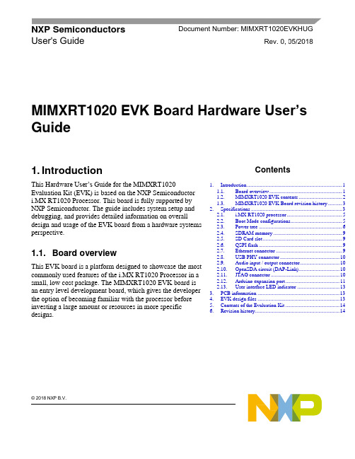
© 2018 NXP B.V.MIMXRT1020 EVK Board Hardware User’sGuide1. IntroductionThis Hardware User’s Guide for the MIMXRT 1020Evaluation Kit (EVK) is based on the NXP Semiconductor i.MX RT1020 Processor. This board is fully supported by NXP Semiconductor. The guide includes system setup and debugging, and provides detailed information on overall design and usage of the EVK board from a hardware systems perspective.1.1. Board overviewThis EVK board is a platform designed to showcase the most commonly used features of the i.MX RT1020 Processor in a small, low cost package. The MIMXRT1020 EVK board is an entry level development board, which gives the developer the option of becoming familiar with the processor before investing a large amount or resources in more specific designs.NXP Semiconductors Document Number: MIMXRT1020EVKHUGUser's GuideRev. 0 , 05/2018Contents1.Introduction ........................................................................ 1 1.1. Board overview ....................................................... 1 1.2. MIMXRT1020 EVK contents ................................. 2 1.3. MIMXRT1020 EVK Board revision history ........... 3 2.Specifications ..................................................................... 3 2.1. i.MX RT1020 processor .......................................... 5 2.2. Boot Mode configurations ....................................... 5 2.3. Power tree ............................................................... 6 2.4. SDRAM memory .................................................... 9 2.5. SD Card slot ............................................................ 9 2.6. QSPI flash ............................................................... 9 2.7. Ethernet connector .................................................. 9 2.8. USB PHY connector ............................................. 10 2.9. Audio input / output connector .............................. 10 2.10. OpenSDA circuit (DAP-Link) ............................... 10 2.11. JTAG connector .................................................... 10 2.12. Arduino expansion port ......................................... 11 2.13. User interface LED indicator ................................ 13 3.PCB information .............................................................. 13 4. EVK design files .............................................................. 13 5. Contents of the Evaluation Kit ......................................... 14 6.Revision history (14)IntroductionFeatures of the MIMXRT1020 EVK board are shown in Table 11.2. MIMXRT1020 EVK contentsThe MIMXRT1020 EVK contains the following items: •MIMXRT1020 EVK Board•USB Cable (Micro B)Specifications 1.3. MIMXRT1020 EVK Board revision history•Rev A: Prototype.2. SpecificationsThis chapter provides detailed information about the electrical design and practical considerations of the EVK Board, and is organized to discuss each block in the following block diagram of the EVK board.( Figure 1)Figure 1. Block diagramThe overview of the MIMXRT1020 EVK Board is shown in Figure 1 & Figure 2.SpecificationsFigure 2. Overview of the MIMXRT1020 EVK Board (Front side)Figure 3. Overview of the MIMXRT1020 EVK Board (Back side)Specifications 2.1. i.MX RT1020 processorThe i.MX RT1020 is a new processor family featuring NXP's advanced implementation of the Arm® Cortex®-M7 Core. It provides high CPU performance and best real-time response. The i.MX RT1020 provides various memory interfaces, including SDRAM, Raw NAND FLASH, NOR FLASH,SD/eMMC, Quad SPI, HyperBus and a wide range of other interfaces for connecting peripherals, such as WLAN, Bluetooth™, GPS. Same as other i.MX processors, i.MX RT1020 also has rich audio features, including SPDIF and I2S audio interface.The i.MX RT1020 applications processor can be used in areas such as industrial HMI, IoT, motor control and home appliances. The architecture's flexibility enables it to be used in a wide variety of other general embedded applications too. The i.MX processor provides all interfaces necessary to connectp eripherals such as WLAN, Bluetooth™, GPS.The more detail information about i.MX RT1020 can be found in the Datasheet and Reference Manual2.2. Boot Mode configurationsThe device has four boot modes (one is reserved for NXP’s use). The boot mode is selected based on the binary value stored in the internal BOOT_MODE register. Switch (SW8-3 & SW8-4) is used to select the boot mode on the MIMXRT1020 EVK Board.Typically, the internal boot is selected for normal boot, which is configured by external BOOT_CFG GPIOs. The following Table 3 shows the typical Boot Mode and Boot Device settings.NOTEFor more information about boot mode configuration, see the System Boot chapter of theMIMXRT1020 Reference Manual. (waiting for update)For more information about MIMXRT1020 EVK boot device selection and configuration, see the main board schematic. (waiting for update)Specifications2.3. Power treeA DC 5 V external power supply is used to supply the MIMXRT1020 EVK Board at J2, and a slide switch SW1 is used to turn the Power ON/OFF. J23 and J9 also can be used to supply the EVK Board. Different power supply need to configure different Jumper setting of J1. Table 4 shows the details:NOTEFor some computers’ USB, it cannot support 500ma before establishingcommunication. In this case, it is recommended to replace the computer oruse the power adapter(J2) to power the EVK Board.The power tree is shown in Figure 4SpecificationsFigure 4. Power TreeThe power control logic of the MIMXRT1020 EVK board is shown in the Figure 5: •It will power up SNVS, and then PMIC_REQ_ON will be switched on to enable external DC/DC to power up other power domains.•ON/OFF button is used to switch ON/OFF PMIC_REQ_ON to control power modes.•RESET button and WDOG output are used to reset the system power.SpecificationsFigure 5. Power Control Diagram The power rails on the board are shown in Table 5.Specifications2.4. SDRAM memoryOne 256 Mb, 166MHz SDRAM (MT48LC16M16A2P) is used on the EVK Board.2.5. SD Card slotThere is a SD card slot(J15) on the MIMXRT1020 EVK Board. J15 is the Micro SD slot for USDHC1 interface. If the developer wants to boot from the SD Card, the boot device switch (SW8) settings should be: OFF, ON, ON, OFF, as shown in Table 3.2.6. QSPI flashA 64 Mbit QSPI Flash is used on the MIMXRT1020 EVK Board. If the developer wants to boot from the QSPI Flash, the boot device switch(SW8) settings should be: OFF, OFF, ON, OFF, as shown in Table 3.2.7. Ethernet connectorThere is one Ethernet Mac controller in the MIMXRT1020 processor. The Ethernet subsystem of the MIMXRT1020 EVK Board is provided by the KSZ8081RNB 10/100M Ethernet Transceiver (U11) and a RJ45 (J14) with integrated Magnetic.Figure 6. Ethernet Connector RJ45Specifications2.8. USB PHY connectorThe MIMXRT1020 contains a integrated USB 2.0 PHYs capable of connecting to USB host/device systems at the USB low-speed (LS) rate of 1.5 Mbits/s, full-speed (FS) rate of 12 Mbits/s or at the USB 2.0 high-speed (HS) rate of 480 Mbits/s.2.9. Audio input / output connectorThe Audio CODEC used on the MIMXRT1020 EVK Board is Wolfson’s Low Power, high quality Stereo Codec, WM8960.The MIMXRT1020 EVK Board include one headphone interface (J11), one onboard MIC (P1), two speaker interfaces (J12, J13). J11 is a 3.5 mm audio stereo headphone jack, which supports jack detect.2.10. OpenSDA circuit (DAP-Link)The OpenSDA circuit (CMSIS–DAP) is an open-standard serial and debug adapter. It bridges serial and debug communications between a USB host and an embedded target processor.CMSIS-DAP features a mass storage device (MSD) bootloader, which provides a quick and easy mechanism for loading different CMSIS-DAP Applications such as flash programmers, run-control debug interfaces, serial-to-USB converters, and more. Two or more CMSIS-DAP applications can run simultaneously. For example, run-control debug application and serial-to-USB converter runs in parallel to provide a virtual COM communication interface while allowing code debugging via CMSIS-DAP with just single USB connection.For the MIMXRT1020 EVK Board, J23 is the connector between the USB host and the target processor. Jumper to serial downloader mode to use stable DAP-Link debugger function. If developer wants to make OpenSDA going to the bootloader mode, and press SW5 when power on. Meanwhile, the OpenSDA supports drag/drop feature for U-Disk. First, use the seral downloader mode and drag/drop the image file to U-Disk. Then select QSPI Flash as boot device and reset the Board, the image will run.2.11. JTAG connectorJ16 is a standard 20-pin/2.54 mm Box Header Connector for JTAG. The pin definitions are shown in Figure 7. Support SWD by default.SpecificationsFigure 7. JTAG pin definitions2.12. Arduino expansion portJ17 – J20 (unpopulated) is defined as Arduino Interface. The pin definitions of Arduino Interface are shown in Table 6.Specifications2.12.1. Power switchSW1 is a slide switch to control the power of the MIMXRT1020 EVK Board when the power supply is from J2. The function of this switch is listed below:•Sliding the switch to the ON position connects the 5 V power supply to the Evaluation board main power system.•Sliding the switch to OFF position immediately removes all power from the board.2.12.2. ON/OFF buttonSW2 is the ON/OFF button for MIMXRT1020 EVK Board. A short pressing in OFF mode causes the internal power management state machine to change state to ON. In ON mode, a short pressing generates an interrupt (intended to be a software-controllable(power-down). An approximate 5 seconds or more pressing causes a forced OFF. Both boot mode inputs can be disconnected.2.12.3. Reset buttonThere are two Reset Button on the EVK Board. SW5 is the Power Reset Button. Pressing the SW5 in the Power On state will force to reset the system power except SNVS domain. The Processor will be immediately turn off and reinitiate a boot cycle from the Processor Power Off state. SW3 is POR Reset Button.EVK design files 2.12.4. USER buttonSW4 is the USER Button(GPIO5-00) for developers using. Pressing can produce changes in high and low levels.2.13. User interface LED indicatorThere are four LED status indicators located on the EVK Board. The functions of these LEDs include: •Main Power Supply(D3)Green: DC 5V main supply is normal.Red: J2 input voltage is over 5.6V.Off: the board is not powered.•Reset RED LED(D15)•OpenSDA LED(D16)•USER LED(D5)3. PCB informationThe MIMXRT1020 EVK Board is made using standard 2-layer technology. The material used was FR-4. The PCB stack-up information is shown in Table 7.4. EVK design filesThe schematics, layout files, and gerber files (including Silkscreen) can be downloaded from/MIMXRT1020-EVK(waiting for update).Revision history5. Contents of the Evaluation KitNOTEPower adaptor, Micro SD Card are not standard parts of the Evaluation Kit.6. Revision historyTable 9 summarizes the changes made to this document since the initial release.Document Number: MIMXRT1020EVKHUGRev. 0 05/2018How to Reach Us: Home Page: Web Support: /supportInformation in this document is provided solely to enable system and softwareimplementers to use NXP products. There are no express or implied copyright licenses granted hereunder to design or fabricate any integrated circuits based on the information in this document. NXP reserves the right to make changes without further notice to any products herein.NXP makes no warranty, representation, or guarantee regarding the suitability of its products for any particular purpose, nor does NXP assume any liability arising out of the application or use of any product or circuit, and specifically disclaims any and all liability, including without limitation consequenti al or incidental damages. “Typical” parameters that may be provided in NXP data sheets and/or specifications can and do vary in different applications, and actual performance may vary over time. All operating parameters, including “typicals”, must be validated for each customer application by customer’s technical experts. NXP does not convey any license under its patent rights nor the rights of others. NXP sells products pursuant to standard terms and conditions of sale, which can be found at the following address: /SalesTermsandConditions . While NXP has implemented advanced security features, all products may be subject to unidentified vulnerabilities. Customers are responsible for the design and operation of their applications and products to reduce the effect of these vulnerabilities oncustomer’s applications and products, and NXP accepts no liability for any vulne rability that is discovered. Customers should implement appropriate design and operating safeguards to minimize the risks associated with their applications and products NXP, the NXP logo, NXP SECURE CONNECTIONS FOR A SMARTER WORLD, , Freescale, the Freescale logo, and Kinetis, are trademarks of NXP B.V. All other product or service names are the property of their respective owners. Arm and Cortex are registered trademarks of Arm Limited (or its subsidiaries) in the EU and/or elsewhere. All rights reserved. © 2018 NXP B.V.。
主板芯片维修技术资料

主板芯片维修技术资料主板芯片级维修技术资料一主板各芯片的功能及名词解释主板芯片组〔chipset〕(pciset) :分为南桥和北桥南桥〔主外〕:即系统I/O芯片〔SI/O〕:主要管理中低速外部设备;集成了中断控制器、DMA控制器。
功能如下:PCI、ISA与IDE之间的通道。
PS/2鼠标控制。
〔间接属南桥管理,直接属I/O管理〕KB控制〔keyboard〕。
(键盘)USB控制。
〔通用串行总线〕SYSTEM CLOCK系统时钟控制。
I/O芯片控制。
ISA总线。
IRQ控制。
〔中断请求〕DMA控制。
〔直接存取〕RTC控制。
IDE的控制。
南桥的连接:ISA—PCICPU—外设之间的桥梁内存—外存北桥〔主内〕:系统控制芯片,主要负责CPU与内存、CPU与AGP之间的通信。
掌控项目多为高速设备,如:CPU、Host Bus。
后期北桥集成了内存控制器、Cache高速控制器;功能如下:CPU与内存之间的交流。
Cache控制。
AGP控制〔图形加速端口〕PCI总线的控制。
CPU与外设之间的交流。
支持内存的种类及最大容量的控制。
〔标示出主板的档次〕内存控制器:决定是否读内存〔高档板集成于北桥〕。
586FX 82438FXVX 82438VXCache:高速缓冲存储器。
〔1〕、high—speed高速〔2〕、容量小主要用于CPU与内存北桥之间加速〔坏时死机,把高速缓冲关掉〕CPUCache内存I/O芯片input/output,〔局部I/O〕。
I/O芯片管理:①LPI〔并口,打印口,PP〕②COM〔串口,鼠标口,SP〕③FDD〔软驱〕④KB控制器〔键盘〕COM口控制芯片:主板上唯一的一个用±12V电源芯片。
串口鼠标问题:1、电源。
2、COM口控制芯片。
3、COM口控制芯片旁的二极管。
BIOS:基本输入输出系统。
〔Basic Input Output System〕主要负责软件、硬件的连接。
既属于硬件,又属于软件,其固化了开机自检程序,以及主板BIOS编写厂家〔Compaq、IBM、Asus等〕的信息。
ZX62R-B-5P中文资料(hirose)中文数据手册「EasyDatasheet - 矽搜」

摇篮
+
DIP
Cradles
ZX80-B-5S ZX80-B-5SA
注:上表列表大会(绝缘体/ 触点 /锁)插头部分1.部件号和相应屏蔽/封面. 注:2.可选印刷电路板插头显示仅供参考.未提供适用连接器. 注意:3上方绝缘子体在大会(绝缘体/ 触点 /锁定)在3D图像列中所示颜色是蓝色清晰度.参考
材料(第2页)为正确颜色.
空白
8
单元
SLD*
SMT 通孔(焊片长:0.8毫米)
大会(绝缘子/触点/锁) 盖(注1)
注1:量词,如A,B,和C *输入.
微型A
微-B
微型AB
2
芯片中文手册,看全文,戳
sConfigurations
配合侧面 组态
应用
安装,终止 款式/导线连接
SMT
标准
SMT
+
DIP 微-B
相反
接触电阻:从10 MO最大初值上升. 插入力:35 N最大,去除力:8 N分钟.
材料
LCP
铜合金 不锈钢
材料 合成树脂
铜合金 不锈钢 不锈钢
sOrdering 信息
qReceptacles
ZX 62 RD - B - 5 P
*8
123
4
56 7 8
qPlugs
ZX 40 - B - 5 S * - 单位
SMT
USB2.0标准 ZX SeriesqMicro-USB接口会议要求
零件号
ZX62-B-5PA(11) ZX62D-B-5PA8
ZX62R-B-5P
三维图像
投递
SMT
ZX62M-B-5P(02)
SMT
Himax HM01B0 UPduino 芯片说明书
HM01B0-UPD-EVNHimax HM01B0 UPduino Shield User GuideFPGA-UG-02081 Version 1.0November 2018Himax HM01B0 UPduino ShieldUser GuideContentsAcronyms in This Document (3)1.Introduction (4)1.1.Further Information (4)2.Power Supply (5)3.Board Overview (5)4.iCE40 UltraPlus Pin Summary (7)5.Software Requirements (9)6.Board Configuration and Programming (9)6.1.Board Configuration (9)6.2.Programming the SPI Flash (10)6.3.Programming the CRAM Directly (11)7.Storage and Handling (13)8.Ordering Information (13)References (14)Technical Support Assistance (14)Appendix A. Himax HM01B0 UPduino Shield Board Schematics (15)Revision History (19)FiguresFigure 1.1. Himax HM01B0 UPduino Shield (4)Figure 3.1. UPduino v2.0 – Front View (5)Figure 3.2. UPduino v2.0 – Back View (5)Figure 3.3. Himax HM01B0 Adapter Board – Front View (6)Figure 3.4. Himax HM01B0 Adapter Board – Back View (6)Figure 6.1. Programming Settings (9)Figure 6.2. Device Family and Device Setting (10)Figure 6.3. Onboard SPI Flash Device Properties Settings (11)Figure 6.4. Device Family and Device Settings (12)Figure 6.5. Device Properties for iCE40 Device Configuration Memory (12)Figure A.1. UPduino 2.0 FPGA Schematic (15)Figure A.2. UPduino 2.0 SPI Flash/I/O Pins/Regulator Connections (16)Figure A.3. UPduino 2.0 FTDI Chip Connection (17)Figure A.4. Himax HM01B0 Adapter Board Schematic (18)TablesTable 4.1. Upstream Connector Mapping (7)Table 8.1. Reference Part Number (13)© 2018 Lattice Semiconductor Corp. All Lattice trademarks, registered trademarks, patents, and disclaimers are as listed at /legal.All other brand or product names are trademarks or registered trademarks of their respective holders. The specifications and information herein are subject to change without notice.2 FPGA-UG-02081-1.0Himax HM01B0 UPduino ShieldUser Guide Acronyms in This DocumentA list of acronyms used in this document.Acronym DefinitionFPGA Field-Programmable Gate ArrayFTDI Future Technology Devices InternationalI²S Inter-IC SoundLED Light-Emitting DiodeSOIC Small Outline Integrated CircuitSPI Serial Peripheral InterfaceUSB Universal Serial Bus© 2018 Lattice Semiconductor Corp. All Lattice trademarks, registered trademarks, patents, and disclaimers are as listed at /legal.All other brand or product names are trademarks or registered trademarks of their respective holders. The specifications and information herein are subject to change without notice. FPGA-UG-02081-1.0 3Himax HM01B0 UPduino ShieldUser Guide© 2018 Lattice Semiconductor Corp. All Lattice trademarks, registered trademarks, patents, and disclaimers are as listed at /legal .All other brand or product names are trademarks or registered trademarks of their respective holders. The specifications and information herein are subject to change without notice.4 FPGA-UG-02081-1.01. IntroductionThe Himax HM01B0 UPduino Shield is an evaluation and development platform based on the iCE40™ UltraPlus FPGA (Field-Programmable Gate Array). It consists of two boards – the UPduino v2.0 and the Himax HM01B0 Aapter Board. The UPduino v2.0 is an efficient, low-cost base platform designed by Gnarly Grey, including the iCE40UP5K FPGA, and basic power and programming control. The Himax HM01B0 Adapter Board adds a camera with a low-power Himax image sensor, two microphones, and multiple LEDs for quick visual feedback.This flexible and powerful platform enables designers to investigate and experiment with key features of the iCE40 UltraPlus FPGA and assists with rapid prototyping and testing of specific designs.Key features of the Himax HM01B0 UPduino Shield include: ∙ UPduino v2.0∙ iCE40 FPGA - iCE40UP5K-SG48I (5K LUTs, 39 I/Os, 120 Kbits Embedded Block RAM, 1 PLL and more in a 7 mm x7 mm 48-pin QFN package.)∙ USB connection for UART and device programming ∙ On-board Boot Flash ∙ RGB LED∙ Himax HM01B0 Adapter Board∙ Camera module with Himax HM01B0 image sensor ∙ Two I 2S microphones ∙ Six green LEDs∙ Also included with the kit∙ 3 ft Micro USB cable for programming and power ∙ QuickStart GuideFigure 1.1. Himax HM01B0 UPduino Shield1.1. Further InformationThis board features an iCE40UP5K-SG48I FPGA. More information about this FPGA can be found on the Lattice web site at: /iCE40UltraPlus . A complete description of this device can be found in iCE40 UltraPlus Family Data Sheet (FPGA-DS-02008).Himax HM01B0 UPduino ShieldUser Guide© 2018 Lattice Semiconductor Corp. All Lattice trademarks, registered trademarks, patents, and disclaimers are as listed at /legal .All other brand or product names are trademarks or registered trademarks of their respective holders. The specifications and information herein are subject to change without notice.FPGA-UG-02081-1.0 52. Power SupplyExternal 5 V Power from the USB Connector (J7) provides power to the entire two board set. Alternately, power can be applied to headers on the UPduino v2.0 board: ∙ J6 - 5.0 V ∙ J9 – Ground3. Board OverviewThe following diagrams show key features of the Himax HM01B0 Adapter and UPduino v2.0 boards.RGB LED iCE40 UltraPlus FPGAMicro USB ConnectorFigure 3.1. UPduino v2.0 –Front ViewUSB uCFigure 3.2. UPduino v2.0 – Back ViewHimax HM01B0 UPduino ShieldUser Guide© 2018 Lattice Semiconductor Corp. All Lattice trademarks, registered trademarks, patents, and disclaimers are as listed at /legal .All other brand or product names are trademarks or registered trademarks of their respective holders. The specifications and information herein are subject to change without notice.6FPGA-UG-02081-1.0Camera Module with Himax HM01B0 Sensor Holes for MicrophoneAudio InputLEDsFigure 3.3. Himax HM01B0 Adapter Board –Front ViewDual I2S MicrophonesFigure 3.4. Himax HM01B0 Adapter Board – Back ViewHimax HM01B0 UPduino ShieldUser Guide© 2018 Lattice Semiconductor Corp. All Lattice trademarks, registered trademarks, patents, and disclaimers are as listed at /legal .All other brand or product names are trademarks or registered trademarks of their respective holders. The specifications and information herein are subject to change without notice.FPGA-UG-02081-1.0 74. iCE40 UltraPlus Pin SummaryThe following is a reference to indicate the connection of the iCE40 UltraPlus FPGA I/O pins on each board. SG48 Function Pin Type Bank Differential Pair UPduino v2.0 Himax HM01B0Adapter 1 VCCIO_2 VCCIO 2 – – – 2 IO B_6a PIO 2 –JP6-16 I2S data 3 IO B_9b DPIO 2 COMP_of_IOB_8a JP6-11 Molex1 – 8: SDA 4 IO B_8a DPIO 2 TRUE_of_IOB_9bJP6-10 Molex1 – 7: SCL5 VCC VCC VCC –– –6 IO B_13b DPIO 1 COMP_of_IOB_12aJP6-8 Molex1 – 5: FVLD7 CDONE CONFIG 1 – LED – D2– 8 creset_b CONFIG 1 – – –9 IO B_16a PIO 1 – JP6-7 Molex1 – 4: TRIG 10 IO B_18a PIO 1 – TP3 – 11 IO B_20a PIO 1 –JP6-6 MCLK12 IO B_22a DPIO 1 TRUE_of_IOB_23b JP6-1 Molex1 – 18: D1 13 IO B_24a DPIO1 TRUE_of_IOB_25bJP6-3RESET_CAM (NC)14 IO B_32a_SPI_SO DPIO/CONFIG_SPI 1 – SPI Flash – SDO – 15 IO B_34a_SPI_SCK DPIO/CONFIG_SPI 1 – SPI Flash – SCK – 16 IO B_35b_SPI_SS DPIO/CONFIG_SPI 1 – SPI Flash – CS – 17 IO B_33b_SPI_SI DPIO/CONFIG_SPI1 – SPI Flash – SDI–18 IO B_31b PIO 1 – JP6- 5 PWDN (NC) 19 IO B_29b PIO 1 – JP6- 4 Molex1 – 16: PCLK 20 IO B_25b_G3 DPIO/GBIN 1 COMP_of_IOB_24a TP4 –21 IO B_23b DPIO 1 COMP_of_IOB_22aJP6- 2 Molex1 – 17: D022 SPI_V CCIO1 VCCIO 1 –– – 23 IOT_37a DPIO/I3C 0 TRUE_of_IOT_36bJP5- 3 D9 24 VPP_2V5 VPP VPP –– – 25 IOT_36b DPIO/I3C 0 COMP_of_IOT_37a JP5- 4 D826 IOT_39a DPIO 0 TRUE_of_IOT_38b JP5- 5 Molex1 – 24: D7 27 IOT_38b DPIO 0 COMP_of_IOT_39aJP5- 6 Molex1 – 23: D628 IOT_41a PIO 0 – JP5- 16 LED5 29 VCCPLL VCCPLL – – – 30 VCC VCC VCC –– –31 IOT_42b DPIO 0 COMP_of_IOT_43a JP5- 9 Molex1 – 20: D3 32 IOT_43a DPIO 0 TRUE_of_IOT_42bJP5- 7 Molex1 – 22: D533 VCCIO_0 VCCIO 0 –– – 34 IOT_44b DPIO 0 COMP_of_IOT_45aJP5- 11 LEDO35 IOT_46b_G0 DPIO/GBIN 0 –JP5- 8 Mole x1 – 21: D436 IOT_48b DPIO 0 COMP_of_IOT_49a JP5- 13 LED237 IOT_45a_G1 DPIO/GBIN 0 TRUE_of_IOT_44b JP5- 10 Molex1 – 19: D238 IOT_50b DPIO 0 COMP_of_IOT_51aJP5- 15 LED4 39 RGB0 LED 0 – RGB LED – Red –40 RGB1 LED 0 – RGB LED – Green – 41 RGB2 LED 0 –RGB LED – Blue– 42 IOT_51a DPIO 0 TRUE_of_IOT_50b JP5- 14 LED3 43IOT_49aDPIOTRUE_of_IOT_48bJP5- 12LED1Himax HM01B0 UPduino ShieldUser Guide© 2018 Lattice Semiconductor Corp. All Lattice trademarks, registered trademarks, patents, and disclaimers are as listed at /legal .All other brand or product names are trademarks or registered trademarks of their respective holders. The specifications and information herein are subject to change without notice.8 FPGA-UG-02081-1.0SG48 Function Pin Type Bank Differential Pair UPduino v2.0 Himax HM01B0Adapter 44 IO B_3b_G6 DPIO/GBIN 2 COMP_of_IOB_2a JP6- 9 Molex1 – 6: LVLD 45 IO B_5b DPIO 2 COMP_of_IOB_4a JP6- 13 U2 – 2: STBY 46 IO B_0a PIO 2 –JP6- 15 I25 Clk 47 IO B_2a DPIO 2 TRUE_of_IOB_3b JP6- 14 I25 WS 48 IO B_4a DPIO 2 TRUE_of_IOB_5bJP6- 12 –Paddle GNDGNDGND––Molex1 – 9: INTHimax HM01B0 UPduino ShieldUser Guide 5.Software RequirementsInstall the following software before you begin developing designs for the board:∙Lattice Radiant 1.0 (or higher)∙Used for developing your own custom designs for the iCE40 UltraPlus FPGA∙Download at: /radiant∙Radiant Programmer 1.0 (or higher)∙Used to program the iCE40 UltraPlus FPGA∙This is included with Radiant software installation, or as a stand-alone tool.∙Download at: /radiant6.Board Configuration and Programming6.1.Board ConfigurationThe iCE40 UltraPlus on Himax HM01B0 UPduino Shield can be programmed via the included micro-USB cable using a PC running Lattice Radiant Programmer software. After the software is installed and launched, and the USB cable is connected to the board, see below for programming procedures.There are two modes to program the iCE40 UltraPlus FPGA on the UPduino v2.0 board.∙SPI Flash Programming (default): In this mode, the on-board SPI Flash is programmed, which in-turn programs the iCE40 UltraPlus FPGA at power-up or reset. This allows the user program to be stored in non-volatile memory when the board is powered-off or reset. This is the default programming mode.∙Direct CRAM Programming: In this mode, the iCE40 UltraPlus FPGA CRAM memory is programmed directly. This may allow for more rapid reconfiguration (if you need to regularly re-program the iCE40 UltraPlus whiledebugging), but the program is not be retained when the board is powered-off. To use this mode, a modification to the board is required.The default programming mode is SPI Flash programming. To change the programming mode, resistor R4 and R3 must be removed and replaced in the orientation shown in Figure 6.1.Figure 6.1. Programming Settings© 2018 Lattice Semiconductor Corp. All Lattice trademarks, registered trademarks, patents, and disclaimers are as listed at /legal.All other brand or product names are trademarks or registered trademarks of their respective holders. The specifications and information herein are subject to change without notice. FPGA-UG-02081-1.0 9Himax HM01B0 UPduino ShieldUser Guide6.2.Programming the SPI FlashTo program the SPI Flash:1.Set board resistors to horizontal for SPI Flash programming.Note: This is the default mode.2.Connect the Himax HM01B0 UPduino Shield via USB cable to PC with Radiant Programmer installed.3.Start Radiant Programmer.4.Set Device Family to iCE40 UltraPlu s and Device to iCE40UP5K as shown in Figure 6.2.Figure 6.2. Device Family and Device Setting5.Click the iCE40 UltraPlus row, and select Edit > Device Properties.6.In the Device Properties dialog box, apply the settings below that are common to the three files to program (seeFigure 6.3).a.Under Device Operation, select the options below:∙Target Memory —External SPI Flash Memory (SPI FLASH)∙Port Interface—SPI∙Access Mode— Direct Programming∙Operation—Erase, Program, Verifyb.Under Programming Options, select the option below:∙Programming File —<Select desired file to program>c.Under SPI Flash Options, select the options below:∙Family —SPI Serial Flash∙Vendor —Winbond∙Device —W25P32∙Package —16-pin SOIC© 2018 Lattice Semiconductor Corp. All Lattice trademarks, registered trademarks, patents, and disclaimers are as listed at /legal.All other brand or product names are trademarks or registered trademarks of their respective holders. The specifications and information herein are subject to change without notice.10 FPGA-UG-02081-1.0Himax HM01B0 UPduino ShieldUser GuideFigure 6.3. Onboard SPI Flash Device Properties Settings7.Click OK to close the Device Properties window.8.Click the Program button in Radiant Programmer to program the Onboard SPI Flash.6.3.Programming the CRAM DirectlyTo program the CRAM directly:1.Set board resistors to vertical for CRAM Programming.2.Connect the Himax HM01B0 UPduino Shield via USB cable to PC with Radiant Programmer installed.3.Start Radiant Programmer.4.Set Device Family to iCE40 UltraPlus and Device to iCE40UP5K as shown in Figure 6.4.5.Click the iCE40 UltraPlus row, and select Edit > Device Properties.© 2018 Lattice Semiconductor Corp. All Lattice trademarks, registered trademarks, patents, and disclaimers are as listed at /legal.All other brand or product names are trademarks or registered trademarks of their respective holders. The specifications and information herein are subject to change without notice. FPGA-UG-02081-1.0 11Himax HM01B0 UPduino ShieldUser GuideFigure 6.4. Device Family and Device Settings6.In the Device Properties dialog box, apply the as shown in Figure 6.5.∙Target Memory —Compressed Random Access Memory (CRAM)∙Port Interface —Slave SPI∙Access Mode — Direct Programming∙Operation —Fast Configuration7.Click OK to close the Device Properties window.8.Click the Program button in Radiant Programmer to begin programming.Figure 6.5. Device Properties for iCE40 Device Configuration Memory© 2018 Lattice Semiconductor Corp. All Lattice trademarks, registered trademarks, patents, and disclaimers are as listed at /legal.All other brand or product names are trademarks or registered trademarks of their respective holders. The specifications and information herein are subject to change without notice.12 FPGA-UG-02081-1.0Himax HM01B0 UPduino ShieldUser Guide© 2018 Lattice Semiconductor Corp. All Lattice trademarks, registered trademarks, patents, and disclaimers are as listed at /legal .All other brand or product names are trademarks or registered trademarks of their respective holders. The specifications and information herein are subject to change without notice.FPGA-UG-02081-1.0 137. Storage and HandlingStatic electricity can shorten the life span of electronic components. Observe these tips to prevent damage that can occur from electrostatic discharge:∙ Use antistatic precautions such as operating on an antistatic mat and wearing an antistatic wristband. ∙ Store the development board in the provided packaging.∙ Touch a metal USB housing to equalize voltage potential between you and the board.8. Ordering InformationDescriptionOrdering Part Number China RoHS Environment-Friendly Use Period (EFUP)Himax HM01B0 UPduino ShieldHM01B0-UPD-EVNHimax HM01B0 UPduino ShieldUser GuideReferencesFor more information, refer to∙iCE40 Ultra Plus Family Data Sheet (FPGA-DS-02008)∙/iCE40UltraPlusTechnical Support AssistanceSubmit a technical support case through /techsupport.© 2018 Lattice Semiconductor Corp. All Lattice trademarks, registered trademarks, patents, and disclaimers are as listed at /legal.All other brand or product names are trademarks or registered trademarks of their respective holders. The specifications and information herein are subject to change without notice.14 FPGA-UG-02081-1.0Himax HM01B0 UPduino ShieldUser Guide Revision HistoryRevision 1.0, November 2018Section Change SummaryAll Initial release.© 2018 Lattice Semiconductor Corp. All Lattice trademarks, registered trademarks, patents, and disclaimers are as listed at /legal. All other brand or product names are trademarks or registered trademarks of their respective holders. The specifications and information herein are subject to change without notice.FPGA-UG-02081-1.0 197th Floor, 111 SW 5th Avenue Portland, OR 97204, USAT 503.268.8000 HM01B0-UPD-EVN。
超强K620系列信创服务器 用户指南说明书
机架式服务器产品说明书——超强K620系列信创服务器用户指南前言前言概述本文档介绍了超强K620鲲鹏服务器的产品外观,结构,组件和规格,指导用户对超强K620进行安装、连线、上电下电、基本配置、安装操作系统及处理故障等操作。
本文档适用于鲲鹏920处理器以下型号:7260、5250、5230、7265、5255、5220和3210。
其中,7260原为6426、5250对原为4826、5230原为3226。
符号约定在本文中可能出现下列标志,它们所代表的含义如下。
目录前言...................................................................................................................................................... i i 1简介 .. (1)1.1 物理结构 (1)1.2 逻辑结构 (3)2组件 (7)2.1 前面板组件 (7)2.2 前面板指示灯和按钮 (10)2.3 后面板组件 (13)2.4 后面板指示灯 (15)2.5 灵活IO 卡 (16)2.6 硬盘编号及指示灯 (17)2.6.1 硬盘编号 (17)2.6.2 SAS/SATA 硬盘指示灯 (21)2.6.3 NVMe 硬盘指示灯 (21)2.7 Riser 卡和PCIe 插槽 (22)2.8 风扇 (28)3产品规格 (30)3.1 技术规格 (30)3.2 环境规格 (33)3.3 物理规格 (35)3.4 电源规格 (35)4软硬件兼容性 (36)5安装与配置 (37)5.1 工具准备 (37)5.2 设备上的标志 (38)5.3 防静电 (39)5.3.1 操作准则 (39)5.3.2 佩戴防静电腕带 (40)5.4 安装环境要求 (40)5.4.1 空间要求与通风要求 (40)5.4.2 温度要求与湿度要求 (41)5.4.3 机柜要求 (41)5.5 拆除机箱外包装 (41)5.6 安装硬件选件 (42)5.7 安装导轨及服务器 (42)5.7.1 安装L 型滑道及服务器 (42)5.7.2 安装可伸缩滑道及服务器 (45)5.8 连接外部线缆 (46)5.8.1 布线指导 (46)5.8.2 连接鼠标、键盘和VGA 接口线缆 (47)5.8.3 连接网线 (48)5.8.4 连接光口线缆 (49)5.8.5 连接USB 设备 (52)5.8.6 连接串口线缆 (53)5.8.7 连接电源线缆 (54)5.8.7.1 连接交流电源线缆 (54)5.8.7.2 连接直流电源线缆 (55)5.8.8 检查线缆连接 (56)5.9 上电与下电 (57)5.10 初始配置 (59)5.10.1 默认数据 (59)5.10.2 配置简介 (60)5.10.3 查询管理网口IP 地址 (61)5.10.4 登录iBMC Web 界面 (64)5.10.5 检查服务器 (65)5.10.6 修改初始密码 (69)5.10.7 配置RAID. (73)5.10.8 设置BIOS. (73)5.10.9 安装操作系统 (81)5.10.10 使系统保持最新状态 (81)6故障处理指导 (83)7维保与安全 (84)7.1 维保与保修 (84)7.2 安全 (84)8常用操作 (85)8.1 登录远程虚拟控制台 (85)8.1.1 通过iBMC WEB 登录服务器远程虚拟控制台 (85)8.1.2 使用独立远程控制台登录服务器实时桌面 (90)8.2 登录iBMC 命令行 (95)8.3 使用PuTTY 登录服务器(串口方式) (98)8.4 使用PuTTY 登录服务器(网口方式) (100)8.5 查询服务器处理器型号 (102)9更多资源 (106)9.1 技术支持 (106)9.2 维护工具 (107)A 附录 (108)A.1 BIOS. (108)A.2 iBMC (109)A.3 术语 (109)A.4 缩略语 (111)A.5 传感器列表(配置鲲鹏920 7260、5250、5230、7265 或5255 处理器) (114)A.6 传感器列表(配置鲲鹏920 5220 或3210 处理器) (117)1 简介超强K620鲲鹏服务器是基于鲲鹏920处理器的数据中心服务器,K620是2U 2路机架服务器。
深圳市粤原点 PIC16F785 HV785 数据手册
深圳市粤原点科技有限公司(Microchip Authorized Design Partner)指定授权总部地址:深圳市福田区福虹路世贸广场C座1103座Add: Room 1103,Block C,World Trade Plaza,9Fuhong Road,Futian District Shen Zhen City电话(tel) :86-755-83666321,83666320,83666325传真(fax) :86-755-83666329Web: E-mail:********************@联系人:马先生,王小姐,汤小姐在线咨询:QQ:42513912MSN:***********************7x24小时在线产品咨询:135******** 137********PIC16F785/HV785数据手册采用双相异步反馈PWM双高速比较器和双运算放大器的20引脚8位CMOS闪存单片机 2006 Microchip Technology Inc.初稿DS41249D_CNDS41249D_CN 第ii 页初稿2006 Microchip Technology Inc.提供本文档的中文版本仅为了便于理解。
请勿忽视文档中包含的英文部分,因为其中提供了有关Microchip 产品性能和使用情况的有用信息。
Microchip Technology Inc.及其分公司和相 关公司、各级主管与员工及事务代理机构对译文中可能存在的任何差错不承担任何责任。
建议参考Microchip Technology Inc.的英文原版文档。
本出版物中所述的器件应用信息及其他类似内容仅为您提供便利,它们可能由更新之信息所替代。
确保应用符合技术规范,是您自身应负的责任。
Microchip 对这些信息不作任何明示或暗示、书面或口头、法定或其他形式的声明或担保,包括但不限于针对其使用情况、质量、性能、适销性或特定用途的适用性的声明或担保。
QBD-CB-UMD-201803280018 曙光天阔I620-G30用户手册V1.3(2)
商标和版权
“SUGON”及图标是曙光信息产业股份有限公司的商标或注册商标。 “中科曙光”及图标是曙光信息产业股份有限公司的商标或注册商标,文中“曙光信息产业股份有限公司”简称“曙 光公司”。 “Intel”、“Xeon”图标是 Intel 公司的注册商标。 “Microsoft”、“Windows”、“Windows Server”及“Windows Server System”是微软公司的商标或注册商标。 上面未列明的本手册提及的其他产品、标志和商标名称也可能是其他公司的商标或注册商标,并由其各自公司、其 他性质的机构或个人拥有。 在本用户手册中描述的随机软件,是基于最终用户许可协议的条款和条件提供的,只能按照该最终用户许可协议的 规定使用和复制。 版权所有©2013 曙光信息产业股份有限公司,所有权利保留。 本手册受到著作权法律法规保护,未经曙光信息产业股份有限公司事先书面授权,任何人士不得以任何方式对本手 册的全部或任何部分进行复制、抄录、删减或将其编译为机读格式,以任何形式在可检索系统中存储,在有线或无 线网络中传输,或以任何形式翻译为任何文字。
声明 4: 【注意】
为减少人身伤害、火灾设备损坏的危险,为机架供电的交流电源分支电路不得超载。请向制定设备布线和安装要 求的电气机构咨询。
声明 5: 【注意】
请使用调节式不间断电源(UPS),以免服务器受到电源波动和临时断电的影响。此设备可防止硬件因电涌和电压 峰值的影响而受损,并且可在电源出现故障时使系统保持正常工作状态。
服务器的连接处。
危险警告声明vii
目录
声明........................................................................................................................................ii 商标和版权.......................................................................................................................... iii 电源相关的操作说明...........................................................................................................iv 危险警告声明.......................................................................................................................vi 目录.................................................................................................................................... viii 插图目录...............................................................................................................................xi 表格目录..............................................................................................................................xv 1 产品简介........................................................................................................................... 1
EMX3 中文产品手册
XLR-8:自适应加速控制实时实际语言显示AuCom希望使你的工作变得很简单,图形显示器在许多情况下,我们不用文字,而是远端显示器安装操作板很容易采用任选的操作板安装电机温度电流电机功率上次起动信息日期和时间性能图SCR导通用户可编程的屏幕跳闸消息可拆卸连接器和独特接线器采用插入式控制接线排,容易安装。
调试速度更快EMX3在设计时考虑到易用性,菜单功能规格EMX3产品系列A B C D E 重量EMX3-0023B156.4124.0(294.6)278.0192.2 3.2222.7(10.58)尺寸和重量EMX3有各种尺寸,可以满足你的应用需求。
参看额定值和尺寸,了解详细信息。
EMX3-0023B ˜ 0105B EMX3-0145B ˜ 0220B EMX3-0255c EMX3-0360c ˜ 0930c EMX3-1200c ˜ 1600c型号mm (英寸)mm (英寸)mm (英寸)mm (英寸)mm (英寸)千克(磅)(6.16) 4.88(11.60)(10.94)(7.57)(7.05)EMX3-0043BEMX3-0050BEMX3-0053BEMX3-0076B(8.77) 3.5 (7.22)EMX3-0097B4.8EMX3-0100BEMX3-0105B额定值电压测量卡电压测量卡便于实时监视电源电压,无需使用外部设备。
电压测量卡可增强欠压保护和过压保护。
手指保护器手指保护器防止人意外接触带电端子,从而保护人身安全。
指保护器适用于EMX3-0145B至EMX3-0220B支持Profibus、DeviceNet Modbus RTU协议,通过易于安装的通附件/其他功能部件关于AuCoMAucom制造厂位于新西兰基督城。
全球销售网IMS2数字软起动器MVS中压软起动器。
- 1、下载文档前请自行甄别文档内容的完整性,平台不提供额外的编辑、内容补充、找答案等附加服务。
- 2、"仅部分预览"的文档,不可在线预览部分如存在完整性等问题,可反馈申请退款(可完整预览的文档不适用该条件!)。
- 3、如文档侵犯您的权益,请联系客服反馈,我们会尽快为您处理(人工客服工作时间:9:00-18:30)。
概述
该产品为电池供电的玩具、低压或者电池供电的运动控制应用提供了一种集成的有刷直流马达驱动解决方案。
电路内部集成了采用N沟和P沟功率MOSFET设计的H桥驱动电路,适合于驱动有刷直流马达或者驱动步进马达的一个绕组。
该电路具备较宽的工作电压范围(从2V到9.6V),最大持续输出电流达到2A,最大峰值输出电流达到 3.5A。
该驱动电路内置过热保护电路。
通过驱动电路的负载电流远大于电路的最大持续电流时,受封装散热能力限制,电路内部芯片的结温将会迅速升高,一旦超过设定值(典型值150℃),内部电路将立即关断输出功率管,切断负载电流,避免温度持续升高造成塑料封装冒烟、起火等安全隐患。
内置的温度迟滞电路,确保电路恢复到安全温度后,才允许重新对电路进行控制。
该驱动电路内置限流保护电路。
当流过功率管的电流超过设定值时,内部电路限流保护电路启动,功率管最大输出电流将被限制在设定值。
该功能可确保电路输出端口与地短路、输出端口之间短路时,电路不烧毁。
特性
●低待机电流(小于0.1uA);
●低静态工作电流;
●集成的H桥驱动电路;
●内置防共态导通电路;
●低导通内阻的功率MOSFET管;
●内置带迟滞效应的过热保护电路(TSD);
●内置限流保护电路,输出对地短路,输出与输出短路,不烧电路;
●抗静电等级:3KV(HBM)。
典型应用
●2-6节AA/AAA干电池供电的玩具马达驱动;
●2-6节镍-氢/镍-镉充电电池供电的玩具马达驱动;
●1-2节锂电池供电的马达驱动
订购信息
应用说明
1、基本工作模式
a)待机模式
在待机模式下,INA=INB=L。
包括驱动功率管在内的所有内部电路都处于关断状态。
电路消耗极低极低的电流。
此时马达输出端OUTA和OUTB 都为高阻状态。
b)正转模式
正转模式的定义为:INA=H,INB=L,此时马达驱动端OUTA输出高电平,马达驱动端OUTB输出低电平时,马达驱动电流从OUTA流入马达,从OUTB流到地端,此时马达的转动定义为正转模式。
c)反转模式
反转模式的定义为:INA=L,INB=H,此时马达驱动端OUTB输出高电平,马达驱动端OUTA输出低电平时,马达驱动电流从OUTB流入马达,从OUTA流到地端,此时马达的转动定义为反转模式。
d)刹车模式
刹车模式的定义为:INA=H,INB=H,此时马达驱动端OUTA以及OUTB都输出低电平,马达内存储的能量将通过OUTA端NMOS管或者OUTB端NMOS快速释放,马达在短时间内就会停止转动。
注意在刹车模式下电路将消耗静态功耗。
e)PWM模式A
当输入信号INA为PWM信号,INB=0或者INA=0,INB为PWM信号时,马达的转动速度将受PWM信号占空比的控制。
在这个模式下,马达驱动电路是在导通和待机模式之间切换,在待机模式下,所有功率管都处于关断状态,马达内部储存的能量只能通过功率MOSFET的体二极管缓慢释放。
注意:在PWM模式A下,当输入信号从高电平跳变为低电平时,按照逻辑要求H桥的4个功率管必须全部进入关断的状态。
MX620B内部设计了关断延迟电路,当输入信号从高电平跳变到低电平时,H桥的NMOS功率管立即关断,而高边的PMOS管仍然会维持30us的导通时间,在此期间电机电流通路如下所示。
f)PWM模式B
当输入信号INA为PWM信号,INB=1或者INA=1,INB为PWM信号时,马达的转动速度将受到PWM信号占空比的控制。
在这个模式下,马达驱动电路输出在导通和刹车模式之间,在刹车模式下马达存储的能量通过低边的NMOS管快速释放。
2、防共态导通电路
在全桥驱动电路中,将半桥内的高边PMOS功率管和低边NMOS功率管同时导通的状态称为共态导通状态。
共态导通将出现一个电源至地的瞬态大电流,该电流会引起额外的功耗损失,极端情况下会烧毁电路。
通过内置死区时间,可避免共态导通。
典型的死区时间为300ns。
3、过热保护电路
当驱动电路结温超过预设温度(典型值为150℃)时,TSD电路开始工作,此时控制电路强制关断所有输出功率管,驱动电路输出进入高阻状态。
TSD电路中设计了热迟滞,只有当电路的结温下降到预设温度(典型值130℃)时,电路返回正常工作状态。
4、限流保护电路
电路内部的比较电路能够实时检测PMOS功率管的导通压降,当导通压降超过内部设定值时,功率管驱动电路将驱动功率PMOS进入线性恒流模式,其最大输出电流由内部电路限制。
结温为27摄氏度时,最大输出电流限制在8A。
结温为140度时,最大输出电流限制在4A。
当输出与地短路或者输出与输出短路时,内部限流保护电路将保护电路不会立即烧毁。
由于短路时所有的功耗都消耗在电路上,因此电路温度急剧上升,电路将立即进入过热关断保护状态。
虽然,在短路状态下电路不会立即烧毁,但如果芯片长期处于短路状态,内部结温过高,将会对芯片的寿命造成一定影响。
5、驱动电路最大持续功耗
该系列马达驱动电路内部均设计有过热保护电路,因此当驱动电路消耗的功耗过大时,电路将进入热关断模式,热关断状态下马达将无法正常工作。
驱动电路最大持续功耗的计算公式为:
P M=(150℃-T A)/θJA
其中150℃为热关断电路预设温度点,T A为电路工作的环境温度(℃),θJA为电路的结到环境的热阻(单位℃/W)。
注意:驱动电路的最大持续功耗与环境温度、封装形式以及散热设计等因素有关,与电路导通内阻并无直接关系。
6、驱动电路功耗
马达驱动电路内部功率MOSFET的导通内阻是影响驱动电路功耗的主要因素。
驱动电路功耗的计算公式为:P D=I L2*R ON其中I L表示马达驱动电路的输出电流,R ON表示功率MOSFET的导通内阻。
注意:功率MOSFET的导通内阻随着温度的升高而升高,在计算电路的最大持续输出电流以及功耗时必须考虑导通内阻的温度特性。
7、驱动电路最大持续输出电流
根据驱动电路的最大持续功耗以及驱动电路功耗可计算出驱动电路的最大持续输出电流,计算公式为:
其中的R ONT为考虑温度特性后的功率MOSFET导通内阻。
注意:驱动电路的最大持续输出电流与环境温度、封装形式、散热设计以及功率MOSFET的导通内阻等因素有关。
8、马达内阻选择
上述分析表明,马达驱动电路的最大持续功耗有限。
如果马达驱动电路所驱动马达内阻极小,其堵转电流超过马达驱动电路所能承受的最大持续输出电流太多,则很容易导致马达驱动电路进入过热关断状态,玩具车在跑动或者反复前进、后退时将出现抖动的现象。
在马达驱动电路选型时,必须考虑马达的内阻.
特别注意事项
1、电源与地反接
将电路的电源与地线反接,将导致电路损坏,严重时会导致塑料封装冒烟。
可考虑在电路的电源端串联一个功率肖特基二极管至电池的正端,可防止由于电池接反引起的电路损坏。
功率肖特基二极管的最大持续电流能力必须大于马达堵转的持续电流,否则肖特基二极管会因为过热而损坏。
功率肖特基二极管的反向击穿电压必须大于最高电源电压,如果反向击穿电压过小,当电池反接时,会击穿肖特基二极管造成烧毁。
2、功率电源VDD对地去耦电容(C1)
驱动电路要求添加的功率电源VDD对地去耦电容C1(参考应用线路图1)主要有两个作用:1)、吸收马达向电源释放的能量,稳定电源电压,避免电路因为过压而击穿;2)、在马达起动或者快速正转、反转切换的瞬间,马达需要瞬间大电流才能迅速启动。
由于电池的响应速度以及连接引线较长,往往不能立即输出瞬态大电流,此时需要依赖靠近马达驱动电路附近的储能电容释放出瞬态大电流。
根据电容的储能特性,电容容值越大,相同时间内的电压波动越小,因此在高压、大电流的应用条件下建议电容C1取值100uF,建议根据具体的应用选择电容值,但是该电容C1取值至少需要 4.7uF。
3、静电防护
电路的输入/输出端口采用了CMOS器件,对静电放电敏感。
虽然设计有静电防护电路,但在运输、包装、加工、储存过程中应该采取防静电措施,尤其是在加工过程中应重点考虑防静电。
4、输出对地短路、输出端短路
电路内部设计有限流保护电路,可以保护电路在遇到短路等异常状况时不会立即损坏。
但切不可将电路长期工作在短路状态下,会对芯片的寿命造成影响。
5、输出对电源短路
在正常工作时,当电路的低电平输出端与电源发生短路时,电路将会被立即损坏。
6、最大峰值电流
电路内部设计了限流电路,在芯片结温较高时,峰值电流较小,此时可能会引起电机正、反切换不能及时响应的情况,在方案评估阶段需要特别注意。
合理选择电机的最大峰值电流。
封装外形尺寸图。