2SC2851中文资料
2SC4331中文资料(renesas)中文数据手册「EasyDatasheet - 矽搜」
芯片中文手册,看全文,戳
为我们客户,
旧公司名称产品目录等资料
接手两者所有业务
因此,尽管旧公司名称防护留这个文件中,它是一个有效 电子文档.我们感谢您理解.
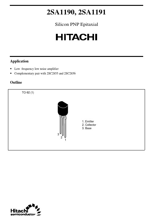
3. 7.5厘米 × 0.7毫米,陶瓷电路板装
封装图(单位: mm)
6.5 ±0.2 5.0 ±0.2 1.5
4
2.3 ±0.2 0.5 ±0.1
1.6 ±0.2 1
2
3
5.5 ±0.2
1.1 ±0.2
13.7最小. 7.0最低
0.5
0.5
2.3 2.3
0.75
TO-251 (MP-3)
6.5 ±0.2 5.0 ±0.2 4.4 ±0.2
8. 你应该使用由瑞萨电子所指定范围内本文档中描述瑞萨电子产品,特别是相对于所述最大额定值,操作电源电压范围,移 动电源电压范围,热辐射特性,安装和其它产品特性.瑞萨电子有权对因使用瑞萨电子产品除这些特定范围故障或损坏 不承担任何责任.
9. 本公司一直致力于提高产品质量和可靠性,半导体产品有 具体特点,如故障以一定速率和故障某些使用条件下发生.进一步, 瑞萨电子产品不受辐射性设计.请一定要采取安全措施,以
芯片中文手册,看全文,戳
注意
1. 本文档中所有信息为发出这份文件日期.这样信息,但是,如有更改恕不另行通知.购买或使用本文中列出任何瑞萨电 子产品前,请确认与瑞萨电子营业部最新产品信息.另外,请大家定期和仔细额外和不同信息由瑞萨电子披露,例如,通 过我们网站披露.
2SK2850-01中文资料

Symbol VDS ID ID(puls] VGS IAR *2 EAS *1 PD Tch Tstg
Ratings 900 ±6 ±24 ±30 6 277 125
+150 -55 to +150
*1 L=14.1mH, Vcc=90V
Unit
V A A V A mJ W °C °C *2 Tch<=150°C
1.0 900
10
Max. Units
V
3.5 V
500
µA
1.0 mA
100
nA
2.50 Ω
S
1450
pF
210
120
30
ns
80
170
90
A
1.5 V
ns
µC
Thermalcharacteristics Item Thermal resistance
Symbol Rth(ch-c)
Rth(ch-a)
Zthch-c [K/W]
Transient thermal impedande Zthch=f(t) parameter:D=t/T
101
100 D=0.5
0.2
0.1 10-1 0.05
0
0.02 0.01
t t
D= T
T
10-2
10-5
10-4
10-3
10-2
10-1
100
101
t [s]
4
100
150
Eas [mJ]
10-1
10-2 0.0 0.2 0.4 0.6 0.8 1.0 1.2 1.4
VSD [V]
100 50 0 0
常用高频管参数与管脚排列
2SC2314 1.8W 17dB 12V 180MHz FM/AM TO-126 E C B
2SC2509 13W 14dB 30MHz WINTransceiver TO-220 B C E
2SC1957 1.8W 17dB 12V 30MHz WINTransceiver TO-126 E C B
2SC1966 9W 7.8dB 13.5V 470MHz FM T-31E
2SC1967 7W 6.7dB 13.5V 470MHz FM T-31E
2N5943 1W 8dB 15V 400MHz FM TO-39
2SC730 0.8W 10dB 13.5V 175MHz FM TO-39 C B E
2SC1096 10W 60MHz FM TO-220
2SC2050 10W 12dB 13.5V 30MHz FM/AM/SSB TO-220 B C E
2SC2053 0.2W 15.7dB 12V 175MHz FM/AM TO-92L B C E
2SC2055 0.25W 15.3dB 12V 175MHz FM/AM TO-92L B C E
2SC2056 1.5W 9dB 12V 175MHz FM TO-39 C B E
2SC2075 4W 13.5V 27MHz WINTransceiver TO-220 B C E
2SC2078 4W 13dB 12V 100MHz FM/AM TO-220 B C E
2SC1675 0.5W 50V 250MHz FM/AM
2SC1678 5W 30MHz WINTransceiver TO-220 B C E
2SC4250中文资料(toshiba)中文数据手册「EasyDatasheet - 矽搜」

反向传输电容 过渡频率 转换增益 噪声系数
(Ta = 25°C)
符号
测试条件
ICBO IEBO V (BR) CEO hFE Cre
fT Gce NF
VCB = 25 V, I E = 0 VEB = 3 V, I C = 0 IC = 1毫安,我B = 0 VCE = 10 V, I C = 5毫安 VCB = 10 V, I E = 0, f = 1兆赫 VCE = 10 V, I C = 5毫安 VCC = 12 V, f = 200兆赫,女 L = 260兆赫 (图1)
• 请联系您的东芝销售代表了解详细信息,以环境问题,如产品的RoHS指令的兼容性. 请遵守产品使用与规范纳入或使用受控物质,包括但不限于,欧盟RoHS指令的所有适用的法律和法规.东芝对发生违规作为适用的法律和法规而导致的损害 或损失不承担任何责任.
5
2007-11-01
• 东芝公司及其子公司和附属公司(统称为“TOSHIBA”),保留这份文件中更改信息的权利,以及相关的硬件,软件和系统(统称为“产品”),恕不另行通 知.
• 本文档以及任何信息均不得转载未经东芝事先书面许可.即使 东芝的书面许可,复制是允许的,只要在没有任何改动/遗漏.
• 虽然东芝的作品不断地提高产品的质量和可靠性,产品会发生故障或失败.客户 负责符合安全标准和用于提供充分的设计和保障其硬件,软件和 这最大限度地降低风险,并避免出现在产品的故障或失效可能导致生命丧失,身体系统 人身伤害或财产损失,包括数据丢失或损坏.在创作和制作的设计和使用,客户必须 也指,符合(一)中的所有相关信息,东芝的最新版本,包括但不限于本文件, 规格,数据表和应用笔记产品的注意事项和条件中规定的“TOSHIBA 半导体可靠性手册“和(b)对于该产品将与或使用的应用程序的说明.客户全权负责自己的产品设计或应用程序的各个方面,包括但不限于:(a)确定 的利用这样的设计或应用该产品的适当性; (b)评价和确定本文档中包含的任何信息的适用性,或图表,图表,程序,算法,示例应用电路,或 任何其他引用文件; (三)验证这样的设计和应用的所有运行参数.
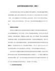
MQO28512Q中文资料
B2-53F EATURES•–55°C to +125°•16 TO 40 VDC input•Four fully regulated outputs •Internal EMI filter meets MIL-STD-461C CE03•Active transient suppressor••Fully isolated•Magnetic feedback•••Inhibit function••Undervoltage lockoutDESCRIPTIONThe MQO Series™of DC/DC converters supply up to 16.5 watts in a four output configuration of ±5 and ±12 or ±5 and ±15 VDC. An integral EMI filter and transient suppressor allow the converters to meet MIL-STD-461C standards without external components. An output hold-up feature provides a low power flag and full output power hold-up through transient dropout conditions.The MQO Series converters are packaged in hermetically sealed cases and are rated for full power operation from –55°to +125°C case temperature. This makes these units ideal for military, aero-space, and hi-rel industrial applications.A high gain bandwidth magnetically isolated control loop is used to precisely regulate the +5 VDC output. Constant frequency pulse width with a single ended forward topology is used. The –5 VDC output and the auxiliary outputs are independently controlled with low headroom regulators, eliminating cross regulation errors. The use of feedforward, compensation, and a high gain bandwidth control loop provides excellent rejection to the conducted audio spectrum of MIL-STD-704A-D and MIL-STD-461C.I NTEGRAL EMI F ILTERThe MQO Series includes a a built-in EMI filter and transient suppressor which allow the units to meet the most common military standards without any external components. The internal EMI filter provides both differential and common mode attenuation on theinput power lines to allow meeting the CE03 interference and CS02 susceptibility requirements. The active internal transient suppressor provides protection against MIL-STD-704A, 1275, and 461C line transients. Protection is provided for transients up to 400 V from a 0.5 ohm source and 600 V from a 50 ohm source.B UILT -I N H OLD -U P F UNCTION WITH F LAGAn output hold-up feature provides a low power flag and full output power hold-up through transient drop out conditions. At full load for a Vin step from 28 to 0 volts, the minimum hold-up time will be 50µs. The low power flag (TTL high) is asserted 10 µs before the end of the hold-up time. External capacitance can be added to extend hold-up time.S HORT C IRCUIT P ROTECTIONMQO Series converters provide predictable current limiters which directly sense output load current in the converter’s secondary.During short circuit or overload conditions, the current limiters provide constant output current and an input power fold-back.U NDERVOLTAGE L OCKOUTUndervoltage lockout prevents the converters from operating below approximately 12 VDC input voltage which helps keep system current levels smooth, especially during initialization or re-start oper-ations.MQO SERIES16 WATTINHIBITTYPICAL CHARACTERISTICSRECOMMENDED OPERATING CONDITIONSABSOLUTE MAXIMUM RATINGSInput Voltage •16 to 40 V Output Power •16.75 wattsLead Soldering Temperature (10 sec per lead)•300°CStorage Temperature Range (Case)•–65°C to +150°CB2-54MQO SERIES 16WATTDC/DC C ONVERTERSUndervoltage Lockout •12 V input typical Isolation•100 megohm minimum at 500 V Audio Rejection •Up to 50 dBConversion Frequency •550 kHz typicalInput Voltage Range•16 to 40 VDC continuousCase Operating Temperature (Tc)•–55°C to +125°C full power •–55°C to +135°C absolute Derating Output Power/Current•Linearly from 100% at 125°C to 0% at 135°CInhibit TTL Open Collector •Logic low (output disabled)•Referenced to input common •Logic high (output enabled)Open collectorMQO28512QMQO28515QPARAMETER CONDITIONMIN TYP MAX MIN TYP MAX UNITSOUTPUT VOLTAGE+5 4.95 5.00 5.05 4.95 5.00 5.05–5 4.95 5.00 5.05 4.95 5.00 5.05+ AUX.11.9012.0012.1014.9015.0015.10VDC– AUX.11.9012.0012.1014.9015.0015.10OUTPUT CURRENT +5390—2000390—2000–50—3500—350+ AUX.0—2080—167mA– AUX.0—2080—167OUTPUT POWER +5 1.95—10.00 1.95—10.00V IN = 16 TO 40 VDC –50— 1.750— 1.75+ AUX.0— 2.500— 2.50W– AUX.0— 2.500— 2.50OUTPUT RIPPLE +5—5055—505510 kHz to 2 MHz –5——30——30+ AUX.——50——50mV p-p– AUX.——50——50LINE REGULATION V IN = 16 TO 36 VDC +5——20——20mV –5, ±AUX.——50——50LOAD REGULATION MINIMUM LOAD TO FULL ±5—20120 —20120 mV±AUX.—50220 —50220INPUT VOLTAGE MINIMUM LOAD TO FULLTc = –55°TO +125°CCONTINUOUS 162840162840VDCTRANSIENT 50ms 0.5 OHM SOURCE ——400——40050 OHM SOURCE ——600——600VINPUT CURRENT MINIMUM LOAD ——230——230FULL LOAD ——960——960mA INHIBITED ——10 —— 10INPUT RIPPLE —50— —50—mA p-p EFFICIENCY 10 kHz TO 2 MHz —64——64—%START-UP DELAY —20——20—msElectrical Characteristics:25°C Tc,28 VDC Vin,100% load,unless otherwise specified.B2-55MQO SERIES16 WATTDC/DC CONVERTERSB2-56MQO SERIES 16 WATTDC/DC C ONVERTERS23624-001-DTS Rev A DQ# 3003All technical information is believed to be accurate, but no responsibility is assumed for errors or omissions. Interpoint reserves the right to make changes in products or specifications without notice. MQO Series is a trademark of Interpoint.Copyright ©1991 - 1999 Interpoint. All rights reserved.CASE N C ASESB8-34C ASESCASE NB8-35TEST (125°C Products)STANDARD/ES/883 (Class H)* PRE-CAP INSPECTIONMethod 2017,2032yes yes yes TEMPERATURE CYCLE (10 times)Method 1010, Cond. C, -65°C to 150°C no no yes Method 1010, Cond. B, -55°C to 125°C no yes no CONSTANT ACCELERATIONMethod 2001, 3000 g no no yes Method 2001, 500 g no yes noBURN-INMethod 1015, 160 hours at 125°C no no yes96 hours at 125°C case (typical)no yes noFINAL ELECTRICAL TEST MIL-PRF-38534, Group ASubgroups 1 through 6: -55°C, +25°C, +125°C no no yes Subgroups 1 and 4: +25°C case yes yes no HERMETICITY TESTINGFine Leak, Method 1014, Cond. A no yes yesGross Leak, Method 1014, Cond. C no yes yesGross Leak, Dip (1 x 10⁻³)yes no noFINAL VISUAL INSPECTIONMethod 2009yes yes yesTest methods are referenced to MIL-STD-883 as determined by MIL-PRF-38534.*883 products are built with element evaluated components and are 100% tested and guaranteed over the full military temperature range of –55°C to +125°C.MOR Series MFLHP Series MFL Series MHP Series MTR Series MQO Series**MHD SeriesMHV SeriesMHF+ SeriesMHF Series**MGA SeriesMSA SeriesMGH SeriesMCH SeriesFM-704A EMI FilterFMD**/FME EMI FilterFMC EMI FilterFMH EMI FilterFMGA EMI FilterFMSA EMI FilterHUM Modules**LCM Modules**LIM ModulesQA SCREENING125°C PRODUCTS125°C P RODUCTSApplies to the following products**MFLHP Series, MQO Series, MHF Series, FMD EMI Filters, Hum Modules, and LCM Modules do not offer ‘883” screening.C2-10。
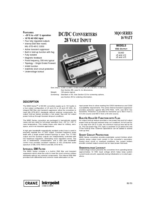
UCC28221D资料
PACKAGING INFORMATIONOrderable Device Status(1)PackageType PackageDrawingPins PackageQtyEco Plan(2)Lead/Ball Finish MSL Peak Temp(3)UCC28220D ACTIVE SOIC D1640Green(RoHS&no Sb/Br)CU NIPDAU Level-1-260C-UNLIMUCC28220DG4ACTIVE SOIC D1640Green(RoHS&no Sb/Br)CU NIPDAU Level-1-260C-UNLIMUCC28220DR ACTIVE SOIC D162500Green(RoHS&no Sb/Br)CU NIPDAU Level-1-260C-UNLIMUCC28220DRG4ACTIVE SOIC D162500Green(RoHS&no Sb/Br)CU NIPDAU Level-1-260C-UNLIMUCC28220PW ACTIVE TSSOP PW1690Green(RoHS&no Sb/Br)CU NIPDAU Level-1-260C-UNLIMUCC28220PWG4ACTIVE TSSOP PW1690Green(RoHS&no Sb/Br)CU NIPDAU Level-1-260C-UNLIMUCC28220PWR ACTIVE TSSOP PW162000Green(RoHS&no Sb/Br)CU NIPDAU Level-1-260C-UNLIMUCC28220PWRG4ACTIVE TSSOP PW162000Green(RoHS&no Sb/Br)CU NIPDAU Level-1-260C-UNLIMUCC28221D ACTIVE SOIC D1640Green(RoHS&no Sb/Br)CU NIPDAU Level-1-260C-UNLIMUCC28221DG4ACTIVE SOIC D1640Green(RoHS&no Sb/Br)CU NIPDAU Level-1-260C-UNLIMUCC28221DR ACTIVE SOIC D162500Green(RoHS&no Sb/Br)CU NIPDAU Level-1-260C-UNLIMUCC28221DRG4ACTIVE SOIC D162500Green(RoHS&no Sb/Br)CU NIPDAU Level-1-260C-UNLIMUCC28221PW ACTIVE TSSOP PW2070Green(RoHS&no Sb/Br)CU NIPDAU Level-1-260C-UNLIMUCC28221PWG4ACTIVE TSSOP PW2070Green(RoHS&no Sb/Br)CU NIPDAU Level-1-260C-UNLIMUCC28221PWR ACTIVE TSSOP PW202000Green(RoHS&no Sb/Br)CU NIPDAU Level-1-260C-UNLIMUCC28221PWRG4ACTIVE TSSOP PW202000Green(RoHS&no Sb/Br)CU NIPDAU Level-1-260C-UNLIM(1)The marketing status values are defined as follows:ACTIVE:Product device recommended for new designs.LIFEBUY:TI has announced that the device will be discontinued,and a lifetime-buy period is in effect.NRND:Not recommended for new designs.Device is in production to support existing customers,but TI does not recommend using this part in a new design.PREVIEW:Device has been announced but is not in production.Samples may or may not be available.OBSOLETE:TI has discontinued the production of the device.(2)Eco Plan-The planned eco-friendly classification:Pb-Free(RoHS),Pb-Free(RoHS Exempt),or Green(RoHS&no Sb/Br)-please check /productcontent for the latest availability information and additional product content details.TBD:The Pb-Free/Green conversion plan has not been defined.Pb-Free(RoHS):TI's terms"Lead-Free"or"Pb-Free"mean semiconductor products that are compatible with the current RoHS requirements for all6substances,including the requirement that lead not exceed0.1%by weight in homogeneous materials.Where designed to be soldered at high temperatures,TI Pb-Free products are suitable for use in specified lead-free processes.Pb-Free(RoHS Exempt):This component has a RoHS exemption for either1)lead-based flip-chip solder bumps used between the die and package,or2)lead-based die adhesive used between the die and leadframe.The component is otherwise considered Pb-Free(RoHS compatible)as defined above.Green(RoHS&no Sb/Br):TI defines"Green"to mean Pb-Free(RoHS compatible),and free of Bromine(Br)and Antimony(Sb)based flame retardants(Br or Sb do not exceed0.1%by weight in homogeneous material)(3)MSL,Peak Temp.--The Moisture Sensitivity Level rating according to the JEDEC industry standard classifications,and peak solder temperature.Important Information and Disclaimer:The information provided on this page represents TI's knowledge and belief as of the date that it is provided.TI bases its knowledge and belief on information provided by third parties,and makes no representation or warranty as to the accuracy of such information.Efforts are underway to better integrate information from third parties.TI has taken and continues to take reasonable steps to provide representative and accurate information but may not have conducted destructive testing or chemical analysis on incoming materials and chemicals.TI and TI suppliers consider certain information to be proprietary,and thus CAS numbers and other limited information may not be available for release.In no event shall TI's liability arising out of such information exceed the total purchase price of the TI part(s)at issue in this document sold by TI to Customer on an annual basis.OTHER QUALIFIED VERSIONS OF UCC28220:•Automotive:UCC28220-Q1NOTE:Qualified Version Definitions:•Automotive-Q100devices qualified for high-reliability automotive applications targeting zero defectsTAPE AND REEL INFORMATION*All dimensions are nominal Device Package Type Package DrawingPinsSPQ Reel Diameter (mm)Reel Width W1(mm)A0(mm)B0(mm)K0(mm)P1(mm)W (mm)Pin1Quadrant UCC28220DR SOICD 162500330.016.4 6.510.3 2.18.016.0Q1UCC28220PWR TSSOPPW 162000330.012.47.0 5.6 1.68.012.0Q1UCC28221DR SOICD 162500330.016.4 6.510.3 2.18.016.0Q1UCC28221PWR TSSOP PW 202000330.016.4 6.957.1 1.68.016.0Q1*All dimensions are nominalDevice Package Type Package Drawing Pins SPQ Length(mm)Width(mm)Height(mm) UCC28220DR SOIC D162500346.0346.033.0 UCC28220PWR TSSOP PW162000346.0346.029.0 UCC28221DR SOIC D162500346.0346.033.0 UCC28221PWR TSSOP PW202000346.0346.033.0IMPORTANT NOTICETexas Instruments Incorporated and its subsidiaries(TI)reserve the right to make corrections,modifications,enhancements,improvements, and other changes to its products and services at any time and to discontinue any product or service without notice.Customers should obtain the latest relevant information before placing orders and should verify that such information is current and complete.All products are sold subject to TI’s terms and conditions of sale supplied at the time of order acknowledgment.TI warrants performance of its hardware products to the specifications applicable at the time of sale in accordance with TI’s standard warranty.Testing and other quality control techniques are used to the extent TI deems necessary to support this warranty.Except where mandated by government requirements,testing of all parameters of each product is not necessarily performed.TI assumes no liability for applications assistance or customer product design.Customers are responsible for their products and applications using TI components.To minimize the risks associated with customer products and applications,customers should provide adequate design and operating safeguards.TI does not warrant or represent that any license,either express or implied,is granted under any TI patent right,copyright,mask work right, or other TI intellectual property right relating to any combination,machine,or process in which TI products or services are rmation published by TI regarding third-party products or services does not constitute a license from TI to use such products or services or a warranty or endorsement e of such information may require a license from a third party under the patents or other intellectual property of the third party,or a license from TI under the patents or other intellectual property of TI.Reproduction of TI information in TI data books or data sheets is permissible only if reproduction is without alteration and is accompanied by all associated warranties,conditions,limitations,and notices.Reproduction of this information with alteration is an unfair and deceptive business practice.TI is not responsible or liable for such altered rmation of third parties may be subject to additional restrictions.Resale of TI products or services with statements different from or beyond the parameters stated by TI for that product or service voids all express and any implied warranties for the associated TI product or service and is an unfair and deceptive business practice.TI is not responsible or liable for any such statements.TI products are not authorized for use in safety-critical applications(such as life support)where a failure of the TI product would reasonably be expected to cause severe personal injury or death,unless officers of the parties have executed an agreement specifically governing such use.Buyers represent that they have all necessary expertise in the safety and regulatory ramifications of their applications,and acknowledge and agree that they are solely responsible for all legal,regulatory and safety-related requirements concerning their products and any use of TI products in such safety-critical applications,notwithstanding any applications-related information or support that may be provided by TI.Further,Buyers must fully indemnify TI and its representatives against any damages arising out of the use of TI products in such safety-critical applications.TI products are neither designed nor intended for use in military/aerospace applications or environments unless the TI products are specifically designated by TI as military-grade or"enhanced plastic."Only products designated by TI as military-grade meet military specifications.Buyers acknowledge and agree that any such use of TI products which TI has not designated as military-grade is solely at the Buyer's risk,and that they are solely responsible for compliance with all legal and regulatory requirements in connection with such use. TI products are neither designed nor intended for use in automotive applications or environments unless the specific TI products are designated by TI as compliant with ISO/TS16949requirements.Buyers acknowledge and agree that,if they use any non-designated products in automotive applications,TI will not be responsible for any failure to meet such requirements.Following are URLs where you can obtain information on other Texas Instruments products and application solutions:Products ApplicationsAmplifiers AudioData Converters AutomotiveDSP BroadbandClocks and Timers Digital ControlInterface MedicalLogic MilitaryPower Mgmt Optical NetworkingMicrocontrollers SecurityRFID TelephonyRF/IF and ZigBee®Solutions Video&ImagingWirelessMailing Address:Texas Instruments,Post Office Box655303,Dallas,Texas75265Copyright©2008,Texas Instruments Incorporated。
2SA1191中文资料
25
100
–0.1
Ta = 75°C –25
30 VCE = –12 V Pulse 10 –1 –3 –10 –30 Collector Current IC (mA) –100
–0.03
25
–0.01 –1
–3 –10 –30 Collector Current IC (mA)
–100
Base to Emitter Saturation Voltage vs. Collector Current –10 Base to emitter saturation voltage VBE (sat) (V) Gain bandwidth product fT (MHz) IC = 10 IB Pulse –3 25 1,000
2
2SA1190, 2SA1191
Electrical Characteristics (Ta = 25°C)
2SA1190 Item Collector to base breakdown voltage Collector to emitter breakdown voltage Emitter to base breakdown voltage Collector cutoff current Emitter cutoff current DC current trnsfer ratio Collector to emitter saturation voltage Base to emitter saturation voltage Symbol V(BR)CBO V(BR)CEO V(BR)EBO I CBO I EBO hFE*
10
1.0
3
0.3
1 –1
ICX285AQ中文资料
Between input clock pins
Voltage difference between vertical clock input pins Hφ1 – Hφ2 Hφ1, Hφ2 – Vφ4
Storage temperature
Guaranteed temperature of performance
∗3 Do not apply a DC bias to the substrate clock and reset gate clock pins, because a DC bias is generated within the CCD.