FPGA可编程逻辑器件芯片XQ5VLX110-1EF1153I中文规格书
FPGA可编程逻辑器件芯片XC5VLX155-1FFG1153I中文规格书
General DescriptionUsing the second generation ASMBL™ (Advanced Silicon Modular Block) column-based architecture, the Virtex-5 family contains five distinct platforms (sub-families), the most choice offered by any FPGA family. Each platform contains a different ratio of features to address the needs of a wide variety of advanced logic designs. In addition to the most advanced, high-performance logic fabric, Virtex-5FPGAs contain many hard-IP system level blocks, including powerful 36-Kbit block RAM/FIFOs, second generation 25x 18 DSP slices,SelectIO™ technology with built-in digitally-controlled impedance, ChipSync™ source-synchronous interface blocks, system monitor functionality, enhanced clock management tiles with integrated DCM (Digital Clock Managers) and phase-locked-loop (PLL) clock generators, and advanced configuration options. Additional platform dependant features include power-optimized high-speed serial transceiver blocks for enhanced serial connectivity, PCI Express® compliant integrated Endpoint blocks, tri-mode Ethernet MACs (Media Access Controllers), and high-performance PowerPC®440 microprocessor embedded blocks. These features allow advanced logic designers to build the highest levels of performance and functionality into their FPGA-based systems. Built on a 65-nm state-of-the-art copper process technology, Virtex-5 FPGAs are a programmable alternative to custom ASIC technology. Most advanced system designs require the programmable strength of FPGAs. Virtex-5 FPGAs offer the best solution for addressing the needs of high-performance logic designers, high-performance DSP designers, and high-performance embedded systems designers with unprecedented logic, DSP ,hard/soft microprocessor, and connectivity capabilities. The Virtex-5 LXT , SXT, TXT , and FXT platforms include advanced high-speed serial connectivity and link/transaction layer capability.Summary of Virtex-5 FPGA Features•Five platforms LX, LXT, SXT , TXT, and FXT−Virtex-5 LX: High-performance general logic applications −Virtex-5 LXT: High-performance logic with advanced serial connectivity−Virtex-5 SXT: High-performance signal processing applications with advanced serial connectivity−Virtex-5 TXT: High-performance systems with double density advanced serial connectivity−Virtex-5 FXT: High-performance embedded systems with advanced serial connectivity•Cross-platform compatibility−LXT, SXT, and FXT devices are footprint compatible in the same package using adjustable voltage regulators•Most advanced, high-performance, optimal-utilization,FPGA fabric−Real 6-input look-up table (LUT) technology −Dual 5-LUT option−Improved reduced-hop routing −64-bit distributed RAM option −SRL32/Dual SRL16 option•Powerful clock management tile (CMT) clocking−Digital Clock Manager (DCM) blocks for zero delay buffering, frequency synthesis, and clock phase shifting −PLL blocks for input jitter filtering, zero delay buffering,frequency synthesis, and phase-matched clock division•36-Kbit block RAM/FIFOs −T rue dual-port RAM blocks−Enhanced optional programmable FIFO logic −Programmable -T rue dual-port widths up to x36-Simple dual-port widths up to x72−Built-in optional error-correction circuitry−Optionally program each block as two independent 18-Kbit blocks•High-performance parallel SelectIO technology − 1.2 to 3.3V I/O Operation−Source-synchronous interfacing using ChipSync™technology−Digitally-controlled impedance (DCI) active termination −Flexible fine-grained I/O banking−High-speed memory interface support•Advanced DSP48E slices−25x 18, two’s complement, multiplication −Optional adder, subtracter, and accumulator −Optional pipelining−Optional bitwise logical functionality −Dedicated cascade connections •Flexible configuration options−SPI and Parallel FLASH interface−Multi-bitstream support with dedicated fallbackreconfiguration logic−Auto bus width detection capability•System Monitoring capability on all devices −On-chip/Off-chip thermal monitoring−On-chip/Off-chip power supply monitoring −JT AG access to all monitored quantities•Integrated Endpoint blocks for PCI Express Designs −LXT, SXT , TXT , and FXT Platforms−Compliant with the PCI Express Base Specification 1.1−x1, x4, or x8 lane support per block−Works in conjunction with RocketIO™ transceivers •Tri-mode 10/100/1000 Mb/s Ethernet MACs −LXT, SXT , TXT , and FXT Platforms−RocketIO transceivers can be used as PHY or connect to external PHY using many soft MII (Media Independent Interface) options•RocketIO GTP transceivers 100Mb/s to 3.75Gb/s −LXT and SXT Platforms•RocketIO GTX transceivers 150Mb/s to 6.5Gb/s −TXT and FXT Platforms •PowerPC 440 Microprocessors −FXT Platform only −RISC architecture −7-stage pipeline−32-Kbyte instruction and data caches included −Optimized processor interface structure (crossbar)•65-nm copper CMOS process technology • 1.0V core voltage•High signal-integrity flip-chip packaging available in standard or Pb-free package optionsDS100 (v5.1) August 21, 2015Product SpecificationTable 1:Virtex-5 FPGA Family MembersDevice Configurable Logic Blocks (CLBs)DSP48ESlices(2)Block RAM BlocksCMTs(4)PowerPCProcessorBlocksEndpointBlocks forPCIExpressEthernetMACs(5)Max RocketIOTransceivers(6)TotalI/OBanks(8)MaxUserI/O(7) Array(Row x Col)Virtex-5Slices(1)MaxDistributedRAM(Kb)18Kb(3)36Kb Max(Kb)GTP GTXXC5VLX3080x304,8003203264321,1522N/A N/A N/A N/A N/A13400 XC5VLX50120x307,2004804896481,7286N/A N/A N/A N/A N/A17560 XC5VLX85120x5412,96084048192963,4566N/A N/A N/A N/A N/A17560 XC5VLX110160x5417,2801,120642561284,6086N/A N/A N/A N/A N/A23800 XC5VLX155160x7624,3201,6401283841926,9126N/A N/A N/A N/A N/A23800 XC5VLX220160x10834,5602,2801283841926,9126N/A N/A N/A N/A N/A23800 XC5VLX330240x10851,8403,42019257628810,3686N/A N/A N/A N/A N/A331,200 XC5VLX20T60x263,1202102452269361N/A124N/A7172 XC5VLX30T80x304,8003203272361,2962N/A148N/A12360 XC5VLX50T120x307,20048048120602,1606N/A1412N/A15480 XC5VLX85T120x5412,960840482161083,8886N/A1412N/A15480 XC5VLX110T160x5417,2801,120642961485,3286N/A1416N/A20680 XC5VLX155T160x7624,3201,6401284242127,6326N/A1416N/A20680 XC5VLX220T160x10834,5602,2801284242127,6326N/A1416N/A20680 XC5VLX330T240x10851,8403,42019264832411,6646N/A1424N/A27960 XC5VSX35T80x345,440520192168843,0242N/A148N/A12360 XC5VSX50T120x348,1607802882641324,7526N/A1412N/A15480 XC5VSX95T160x4614,7201,5206404882448,7846N/A1416N/A19640 XC5VSX240T240x7837,4404,2001,0561,03251618,5766N/A1424N/A27960 XC5VTX150T200x5823,2001,500804562288,2086N/A14N/A4020680 XC5VTX240T240x7837,4402,4009664832411,6646N/A14N/A4820680 XC5VFX30T80x385,12038064136682,4482114N/A812360 XC5VFX70T160x3811,2008201282961485,3286134N/A1619640 XC5VFX100T160x5616,0001,2402564562288,2086234N/A1620680 XC5VFX130T200x5620,4801,58032059629810,7286236N/A2024840 XC5VFX200T240x6830,7202,28038491245616,4166248N/A2427960 Notes:1.Virtex-5 FPGA slices are organized differently from previous generations. Each Virtex-5 FPGA slice contains four LUTs and four flip-flops (previouslyit was two LUTs and two flip-flops.)2.Each DSP48E slice contains a 25x18 multiplier, an adder, and an accumulator.3.Block RAMs are fundamentally 36Kbits in size. Each block can also be used as two independent 18-Kbit blocks.4.Each Clock Management Tile (CMT) contains two DCMs and one PLL.5.This table lists separate Ethernet MACs per device.6.RocketIO GTP transceivers are designed to run from 100Mb/s to 3.75Gb/s. RocketIO GTX transceivers are designed to run from 150Mb/s to6.5Gb/s.7.This number does not include RocketIO transceivers.8.Includes configuration Bank 0.Virtex-5 TXT and FXT Platform FeaturesThis section describes blocks only available in TXT and FXT devices.RocketIO GTX Serial TransceiversOne or Two PowerPC 440 Processor Cores(FXT only)(TXT/FXT)8-48 channels RocketIO serial transceivers capable ofrunning 150Mb/s to 6.5Gb/sVirtex-5 Family OverviewVirtex-5 Family OverviewVirtex-5FPGA Ordering InformationVirtex-5 FPGA ordering information shown in Figure1 applies to all packages including Pb-Free.Figure 1:Virtex-5 FPGA Ordering Information。
FPGA可编程逻辑器件芯片XQ5VFX100T中文规格书

TDO_0
PROGRAM_B
CCLK_0
TCK_0
TMS
The RocketIO™ GTP transceiver I/O channels for the devices listed in Table 1-3 or the GTX transceiver I/O channels for the devices listed in Table 1-4.
Table 1-1: Flip-Chip Packages
Package
Packages
Specifications FF323 FF324 FF665 FF676 FF1136 FF1153 FF1156
Pitch (mm) 1.00 1.00 1.00 1.00 1.00 1.00
1.00
Size (mm) 19 x 19 19 x 19 27 x 27 27 x 27 35 x 35 35 x 35 35 x 35
H13
24 IO_L7P_24
H10
24 IO_L7N_24
J10
24 IO_L8P_CC_24
H14
24 IO_L8N_CC_24(2 )
H15
24 IO_L9P_CC_24
K10
Virtex-5 FPGA Packaging and Pinout Specification
Maximum I/Os
172
220
360
440
640
800
360
FF1738 1.00 42.5 x 42.5
960
FF1759 1.00 42.5 x 42.5
680
FF1760 1.00 42.5 x 42.5
FPGA可编程逻辑器件芯片XC5VLX50-1FFG1153I中文规格书

4.08
XC5VLX85
3.52
3.78
4.20
XC5VLX85T
3.52
3.78
4.20
XC5VLX110
3.57
3.84
4.27
XC5VLX110T
3.57
3.84
4.27
XC5VLX155
3.83
4.10
4.53
XC5VLX155T
3.83
4.10
4.53
XC5VLX220
N/A
4.33
4.76
6. TRCKO_FLAGS includes the following parameters: TRCKO_AEMPTY, TRCKO_AFULL, TRCKO_EMPTY, TRCKO_FULL, TRCKO_RDERR, TRCKO_WRERR. 7. TRCKO_POINTERS includes both TRCKO_RDCOUNT and TRCKO_WRCOUNT. 8. The ADDR setup and hold must be met when EN is asserted even though WE is deasserted. Otherwise, block RAM data corruption is possible.
Table 94: Global Clock Setup and Hold With PLL in System-Synchronous Mode
Symbol
Description
Device
Speed Grade
-3
-2
-1
Input Setup and Hold Time Relative to Global Clock Input Signal for LVCMOS25 Standard.(1)
FPGA可编程逻辑器件芯片XQ5VFX130T-1F1738C中文规格书

48
96 48 1,728 6 不适用 不适用 不适用 不适用 不适用 17 560
XC5VLX85
120 x 54 12,960
840
48
192 96 3,456 6 不适用 不适用 不适用 不适用 不适用 17 560
XC5VLX110 XC5VLX155
160 x 54 17,280 160 x 76 24,320
XC5VLX330 240 x 108 51,840 3,420
192 576 288 10,368 6 不适用 不适用 不适用 不适用 不适用 33 1,200
XC5VLX20T 60 x 26 3,120
210
24
52 26 936 1 不适用
1
2
4 不适用 7 172
XC5VLX30T 80 x 30 4,800
DS100 (v5.0) 2009 年 2 月 6 日 产品规范
Virtex-5 系列概述
数控阻抗 (DCI) 有源 I/O 终端 • 可选串行或并行终端 • 温度和电压补偿 • 显著简化电路板布局
- 减少电阻器 - 在理想的位置设置终端,比如信号源或信号终点
65nm 铜 CMOS 工艺
• 1.0V 内核电压 • 12 层金属提供最强的布线功能,并可容纳硬 IP 植入 • 三栅极氧化层技术,确实可降低静态功耗
1,120 1,640
64
256 128 4,608 6 不适用 不适用 不适用 不适用 不适用 23 800
128 384 192 6,912 6 不适用 不适用 不适用 不适用 不适用 23 800
XC5VLX220 160 x 108 34,560 2,280
FPGA可编程逻辑器件芯片XQ5VLX155T-2EF1136I中文规格书

General DescriptionThe Defense-grade XQ UltraScale™ architecture-based devices extend the equivalent commercial offerings, adding unique ruggedized packages, extended operating temperature range support, and added environmental qualification testing. This XQ portfolio spans the following families, with each offering a unique mix of features. XQ Kintex® UltraScale FPGAs: High-performance FPGAs with a focus on price/performance, using both monolithic andnext-generation stacked silicon interconnect (SSI) technology. High DSP and block RAM-to-logic ratios and next-generation transceivers, combined with low-cost packaging, enable an optimum blend of capability and cost.XQ Kintex UltraScale+™ FPGAs: Increased performance and on-chip UltraRAM memory to reduce BOM cost. The ideal mix of high-performance peripherals and cost-effective system implementation. Kintex UltraScale+ FPGAs have numerous power options that deliver the optimal balance between the required system performance and the smallest power envelope.XQ Virtex® UltraScale+ FPGAs: The highest transceiver bandwidth, highest DSP count, and highest on-chip and in-package memory available in the UltraScale architecture. Virtex UltraScale+ FPGAs also provide numerous power options that deliver the optimal balance between the required system performance and the smallest power envelope.XQ Zynq® UltraScale+ MPSoCs: Combine the Arm® v8-based Cortex®-A53 high-performance energy-efficient 64-bit application processor with the Arm Cortex-R5 real-time processor and the UltraScale architecture to create the industry's first Defense-grade MPSoCs. Provide unprecedented power savings, heterogeneous processing, and programmable acceleration. XQ Zynq UltraScale+ RFSoCs: Combine RF data converter subsystem and forward error correction with industry-leading programmable logic and heterogeneous processing capability. Integrated RF-ADCs, RF-DACs, and soft-decision FECs (SD-FEC) provide the key subsystems for multiband, multi-mode cellular radios and cable infrastructure.XQ Device ComparisonsDS895 (v2.0) November 15, 2018Product Specification Table 1:Device Resources(1)XQ Kintex UltraScale FPGAXQ KintexUltraScale+FPGAXQ VirtexUltraScale+FPGAXQ ZynqUltraScale+MPSoCXQ ZynqUltraScale+RFSoCMPSoC Processing System✓✓RF-ADC/DAC and SD-FEC✓System Logic Cells (K)530–1,451475–1,143862–2,835154–1,143930 Block Memory (Mb)21.1–75.916.9–34.625.3–70.9 5.1–34.638.0 UltraRAM (Mb)18–3690–2700–3622.5 HBM DRAM (GB)0(2)DSP (Slices)1,920–5,5201,824–1,9682,280–9,216360–3,5284,272 DSP Performance (GMAC/s)(3)7,2973,05014,2845,4686,621 Transceivers16–6416–5640–960–488–16 Max. Transceiver Speed (Gb/s)16.328.228.228.228.2 Max. Serial Bandwidth (full duplex) (Gb/s)2,0862,4025,4161,950902I/O Pins312–728280–512416–83282–644152–408 Notes:1.Metrics given in this table pertain to the XQ ruggedized package devices. For non-ruggedized device variants consult Xilinx sales.2.HBM not currently offered in an XQ ruggedized Package; consult Xilinx sales for further details and options.3.Calculated based on XQ maximum DSP clock rate for a Symmetric FIR Filter, e.g. for KU040 with 1920 DSP48s, -2 speed-grade DSP48F MAX=661MHz, GMACs=2x0.661x1,920=2,538.XQ Kintex UltraScaleXQ Kintex UltraScale+XQ Virtex UltraScale+XQ Zynq UltraScale+ PLXQ Zynq UltraScale+ PSADC10-bit 200kSPS10-bit 200kSPS10-bit 1MSPS Interfaces JTAG, I2C, DRP JTAG, I2C, DRP, PMBus APB•64-bit quad-core Arm Cortex-A53 MPCores. Features associated with each core include: o Arm v8-A Architectureo Operating target frequency: up to 1.5GHzo Single and double precision floating point:4SP/2DP FLOPso NEON Advanced SIMD support with single and double precision floating point instructions o A64 instruction set in 64-bit operating mode, A32/T32 instruction set in 32-bit operating mode o Level 1 cache (separate instruction and data, 32KB each for each Cortex-A53 CPU)–2-way set-associative Instruction Cache with parity support–4-way set-associative Data Cache with ECC supporto Integrated memory management unit (MMU) per processor coreMIO OverviewThe IOP peripherals communicate to external devices through a shared pool of up to 78 dedicated multiplexed I/O (MIO) pins. Each peripheral can be assigned one of several pre-defined groups of pins, enabling a flexible assignment of multiple devices simultaneously. Although 78 pins are not enough for simultaneous use of all the I/O peripherals, most IOP interface signals are available to the PL, allowing use of standard PL I/O pins when powered up and properly configured. Extended multiplexed I/O (EMIO) allows unmapped PS peripherals to access PL I/O.Port mappings can appear in multiple locations. For example, there are up to 12 possible port mappings for CAN pins. The PS Configuration Wizard (PCW) tool aids in peripheral and static memory pin mapping. See Table 17.Transceiver (PS-GTR)The four PS-GTR transceivers, which reside in the full power domain (FPD), support data rates of up to 6.0Gb/s. All the protocols cannot be pinned out at the same time. At any given time, four differential pairs can be pinned out using the transceivers. This is user programmable via the high-speed I/O multiplexer (HS-MIO). •A Quad transceiver PS-GTR (TX/RX pair) able to support following standards simultaneouslyo x1, x2, or x4 lane of PCIe at Gen1 (2.5Gb/s) or Gen2 (5.0Gb/s) rates o 1 or 2 lanes of DisplayPort (TX only) at 1.62Gb/s, 2.7Gb/s, or 5.4Gb/s o 1 or 2 SATA channels at 1.5Gb/s, 3.0Gb/s, or 6.0Gb/s o 1 or 2 USB3.0 channels at 5.0Gb/s o1-4 Ethernet SGMII channels at 1.25Gb/sTable 17:MIO Peripheral Interface MappingPeripheral InterfaceMIOEMIOQuad-SPI NAND YesNo USB2.0: 0,1Yes: External PHY No SDIO 0,1Yes Yes SPI: 0,1I2C: 0,1CAN: 0,1GPIOYesCAN: External PHY GPIO: Up to 78 bits YesCAN: External PHY GPIO: Up to 96 bitsGigE: 0,1,2,3RGMII v2.0: External PHYSupports GMII, RGMII v2.0 (HSTL), RGMII v1.3, MII, SGMII, and 1000BASE-X in Programmable LogicUART: 0,1Simple UART:Only two pins (TX and RX)Full UART (TX, RX, DTR, DCD, DSR, RI, RTS, and CTS) requires either:•Two Processing System (PS) pins (RX and TX) through MIO and sixadditional Programmable Logic (PL) pins, or •Eight Programmable Logic (PL) pinsDebug Trace Ports Yes: Up to 16 trace bits Yes: Up to 32 trace bits Processor JTAGYesYes。
FPGA可编程逻辑器件芯片XQ5VLX85-1EF676I中文规格书
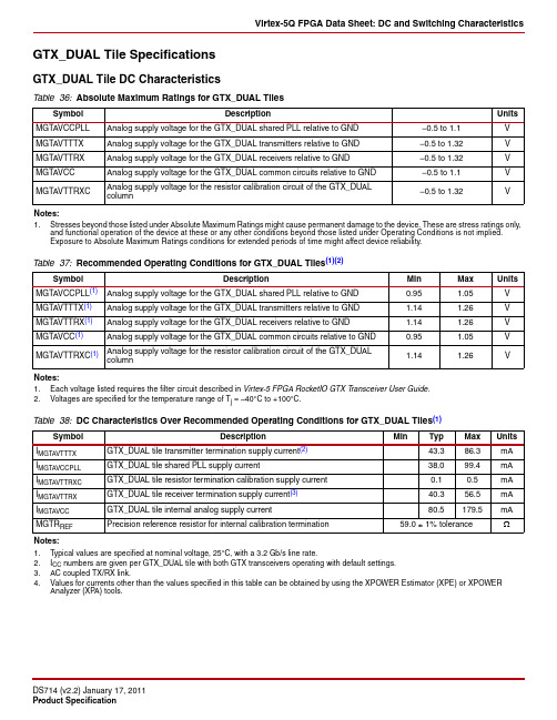
GTX_DUAL Tile SpecificationsGTX_DUAL Tile DC CharacteristicsTable 36:Absolute Maximum Ratings for GTX_DUAL TilesSymbol Description Units MGTAVCCPLL Analog supply voltage for the GTX_DUAL shared PLL relative to GND–0.5 to 1.1V MGTAVTTTX Analog supply voltage for the GTX_DUAL transmitters relative to GND–0.5 to 1.32V MGTAVTTRX Analog supply voltage for the GTX_DUAL receivers relative to GND–0.5 to 1.32V MGTAVCC Analog supply voltage for the GTX_DUAL common circuits relative to GND–0.5 to 1.1VMGTAVTTRXC Analog supply voltage for the resistor calibration circuit of the GTX_DUALcolumn–0.5 to 1.32VNotes:1.Stresses beyond those listed under Absolute Maximum Ratings might cause permanent damage to the device. These are stress ratings only,and functional operation of the device at these or any other conditions beyond those listed under Operating Conditions is not implied.Exposure to Absolute Maximum Ratings conditions for extended periods of time might affect device reliability.Table 37:Recommended Operating Conditions for GTX_DUAL Tiles(1)(2)Symbol Description Min Max Units MGTAVCCPLL(1)Analog supply voltage for the GTX_DUAL shared PLL relative to GND0.95 1.05V MGTAVTTTX(1)Analog supply voltage for the GTX_DUAL transmitters relative to GND 1.14 1.26V MGTAVTTRX(1)Analog supply voltage for the GTX_DUAL receivers relative to GND 1.14 1.26V MGTAVCC(1)Analog supply voltage for the GTX_DUAL common circuits relative to GND0.95 1.05VMGTAVTTRXC(1)Analog supply voltage for the resistor calibration circuit of the GTX_DUALcolumn1.14 1.26VNotes:1.Each voltage listed requires the filter circuit described in Virtex-5 FPGA RocketIO GTX Transceiver User Guide.2.Voltages are specified for the temperature range of T j=–40°C to +100°C.Table 38:DC Characteristics Over Recommended Operating Conditions for GTX_DUAL Tiles(1) Symbol Description Min Typ Max Units I MGTAVTTTX GTX_DUAL tile transmitter termination supply current(2)43.386.3mA I MGTAVCCPLL GTX_DUAL tile shared PLL supply current38.099.4mA I MGTAVTTRXC GTX_DUAL tile resistor termination calibration supply current0.10.5mA I MGTAVTTRX GTX_DUAL tile receiver termination supply current(3)40.356.5mA I MGTAVCC GTX_DUAL tile internal analog supply current80.5179.5mA MGTR REF Precision reference resistor for internal calibration termination59.0 ±1% tolerance Notes:1.T ypical values are specified at nominal voltage, 25°C, with a 3.2Gb/s line rate.2.I CC numbers are given per GTX_DUAL tile with both GTX transceivers operating with default settings.3.AC coupled TX/RX link.4.Values for currents other than the values specified in this table can be obtained by using the XPOWER Estimator (XPE) or XPOWERAnalyzer (XP A) tools.Table 39:GTX_DUAL Tile Quiescent Supply CurrentSymbol Description Typ(1)Max Units I AVTTTXQ Quiescent MGTAVTTTX (transmitter termination) supply current8.221.6mA I AVCCPLLQ Quiescent MGTAVCCPLL (PLL) supply current0.8 4.8mAI AVTTRXQ Quiescent MGTAVTTRX (receiver termination) supply current. IncludesMGTAVTTRXCQ.1.212.0mAI AVCCQ Quiescent MGTAVCC (analog) supply current9.050.4mASystem Monitor Analog-to-Digital Converter SpecificationTable 51:Analog-to-Digital SpecificationsParameter Symbol Comments/Conditions Min Typ Max UnitsAV DD=2.5V±2%,V REFP=2.5V, V REFN=0V, ADCCLK=5.2MHz, T A=T MIN to T MAX, Typical values at T A=+25°CDC Accuracy: All external input channels such as V P/V N and V AUXP[15:0]/V AUXN[15:0], Unipolar Mode,and Common Mode = 0VResolution10Bits Integral Nonlinearity INL±2LSBsDifferential Nonlinearity DNL No missing codes (T MIN to T MAX)Guaranteed Monotonic±0.9LSBs Unipolar Offset Error(1)Uncalibrated±2±30LSBs Bipolar Offset Error(1)Uncalibrated measured in bipolar mode ±2±30LSBs Gain Error(1)Uncalibrated, T j=–40°C to 100°C±0.2±2.0%Uncalibrated, T j=–55°C to 125°C±0.2±2.5% Bipolar Gain Error(1)Uncalibrated measured in bipolar mode,T j=–40°C to 100°C±0.2±2.0%Uncalibrated measured in bipolar mode,T j=–55°C to 125°C±0.2±2.5%T otal Unadjusted Error (Uncalibrated)TUE Deviation from ideal transfer function.V REFP–V REFN=2.5V±10LSBsT otal Unadjusted Error (Calibrated)TUE Deviation from ideal transfer function.V REFP–V REFN=2.5V±1±2LSBsCalibrated Gain T emperature Coefficient Variation of FS code with temperature±0.01LSB/°CDC Common-Mode Reject CMRR DC V N = V CM=0.5V± 0.5V,V P–V N=100mV70dB Conversion Rate(2)Conversion Time - Continuous t CONV Number of CLK cycles2632 Conversion Time - Event t CONV Number of CLK cycles21T/H Acquisition Time t ACQ Number of CLK cycles4DRP Clock Frequency DCLK DRP clock frequency8250MHz ADC Clock Frequency ADCCLK Derived from DCLK, T j=–40°C to 100°C1 5.2MHzDerived from DCLK, T j=–55°C to 125°C 2.5 5.2MHz CLK Duty cycle4060% Analog Inputs(3)Dedicated Analog Inputs Input Voltage RangeV P - V N Unipolar Operation01V Differential Inputs–0.25+0.25 Unipolar Common Mode Range (FS input)0+0.5 Differential Common Mode Range (FS input) +0.3+0.7 Bandwidth20MHzAuxiliary Analog InputsInput Voltage RangeV AUXP[0] /V AUXN[0] to V AUXP[15] /V AUXN[15]Unipolar Operation01Volts Differential Operation–0.25+0.25 Unipolar Common Mode Range (FS input)0+0.5 Differential Common Mode Range (FS input)+0.3+0.7 Bandwidth10kHzInput Leakage Current A/D not converting, ADCCLK stopped±1.0µA Input Capacitance10pF On-chip Supply Monitor Error V CCINT and V CCAUX with calibration enabled±1.0%ReadingDescriptionRegister-to-Register(with I/O Delays)Units Speed Grade-2I-1I-1MBasic Functions16:1 Multiplexer500450450MHz 32:1 Multiplexer500450450MHz 64:1 Multiplexer467407407MHz 9x9 Logic Multiplier with 4 pipestages438428428MHz 9x9 Logic Multiplier with 5 pipestages500428428MHz 16-bit Adder500450450MHz 32-bit Adder500447447MHz 64-bit Adder377323323MHz Register to LUT to Register500450450MHz 16-bit Counter500450450MHz 32-bit Counter500450450MHz 64-bit Counter381333333MHz MemoryCascaded block RAM (64K)450400400MHz Block RAM PipelinedSingle-Port 512x36 bits500450450MHz Single-Port 4096x4 bits500450450MHz Dual-Port A: 4096x4 bits and B: 1024x18 bits500450450MHz。
FPGA可编程逻辑器件芯片XC5VLX110T-2FFG1136I中文规格书
OverviewThe purpose of this notification is to inform Xilinx customers of the discontinuation of certain Virtex®-4 andVirtex®-5 FPGA devices special part numbers only; devices will continue to ship without change to form, fit, or function, but with updated part numbers.DescriptionSince the introduction of Virtex-4 and Virtex-5 FPGA products, Xilinx has qualified both product families in both Toshiba, in Oita, Japan, and UMC in Taiwan, and has been shipping the majority of devices in each product family from UMC. As part of the consolidation effort described in XCN11030, wafer fabrication for all Virtex-4 and Virtex-5 Devices described in this document will be transferred to UMC.As a result of this transfer, certain part numbers, including SCD and Stepping, will be converted into standard part numbers.For these devices, there is no change to the form, fit, or function of the devices themselves. Qualification data is available in the Xilinx reliability report UG116.Products AffectedThe products affected include all Virtex-4 and Virtex-5 part numbers associated with the following associated SCDand stepping: 0641, 0988, 4009, 4013, 4023, 4058, 4094, 4098, 4108, CS1, CS2 part numbers listed in Table 1,Table 2 and Table 3 below.XCN11031 (v1.1) June 9, 2015Product Discontinuation Notice For Virtex-4 and Virtex-5 FPGA SCDs from Toshiba Wafer FabricationXCN11031 (v1.1) June 9, 2015Product Discontinuation Notice For Virtex-4 and Virtex-5 FPGA SCDs from Toshiba Wafer FabricationXCN11031 (v1.1) June 9, 2015Product Discontinuation Notice For Virtex-4 and Virtex-5 FPGA SCDs from Toshiba Wafer FabricationXCN11031 (v1.1) June 9, 2015Product Discontinuation Notice For Virtex-4 and Virtex-5 FPGA SCDs from Toshiba Wafer Fabrication XCN11031 (v1.1) June 9, 2015。
FPGA可编程逻辑器件芯片XQ5VFX70T-2EF1136I中文规格书
Input/Output Delay Switching CharacteristicsCLB Switching CharacteristicsTable 64:Input/Output Delay Switching CharacteristicsSymbolDescriptionSpeed Grade Units-2I-1I-1MIDELAYCTRL T IDELAYCTRLCO_RDY Reset to Ready for IDELAYCTRL 3.00 3.00 3.00µs F IDELAYCTRL_REF REFCLK frequency 200.00200.00200.00MHz IDELAYCTRL_REF_PRECISION REFCLK precision±10±10±10MHz T IDELAYCTRL_RPW Minimum Reset pulse width50.0050.0050.00nsIODELAYT IDELAYRESOLUTIONIODELAY Chain Delay Resolution1/(64x F REF x 1e 6)(1)ps T IDELAYP AT_JITPattern dependent period jitter in delay chain for clock pattern000Note 2Pattern dependent period jitter in delay chain for random data pattern (PRBS 23)±5±5±5Note 2T IODELAY_CLK_MAX Maximum frequency of CLK input to IODELAY 250250250MHz T IODCCK_CE / T IODCKC_CE CE pin Setup/Hold with respect to CK 0.34–0.060.42–0.060.42–0.06ns T IODCK_INC / T IODCKC_INC INC pin Setup/Hold with respect to CK 0.200.040.240.060.240.06ns T IODCK_RST / T IODCKC_RST RST pin Setup/Hold with respect to CK0.28–0.120.33–0.120.33–0.12nsT IODDO_T TSCONTROL delay to MUXE/MUXF switching and through IODELAYNote 3Note 3Note 3T IODDO_IDA TAIN Propagation delay through IODELAY Note 3Note 3Note 3T IODDO_ODA TAIN Propagation delay through IODELAYNote 3Note 3Note 3Notes:Table 65:CLB Switching CharacteristicsSymbol DescriptionSpeed GradeUnits-2I-1I-1MCombinatorial Delays T ILOAn –Dn LUT address to A0.090.100.10ns, Max An –Dn LUT address to AMUX/CMUX 0.220.250.25ns, Max An –Dn LUT address to BMUX_A0.350.400.40ns, Max T ITO An –Dn inputs to A –D Q outputs 0.770.900.90ns, Max T AXA AX inputs to AMUX output 0.440.530.53ns, Max T AXB AX inputs to BMUX output 0.520.610.61ns, Max T AXC AX inputs to CMUX output 0.360.420.42ns, Max T AXD AX inputs to DMUX output 0.620.730.73ns, Max T BXBBX inputs to BMUX output0.410.480.48ns, MaxCLB Distributed RAM Switching Characteristics (SLICEM Only)CLB Shift Register Switching Characteristics (SLICEM Only)Table 66:CLB Distributed RAM Switching CharacteristicsSymbol DescriptionSpeed GradeUnits-2I-1I-1MSequential Delays T SHCKO Clock to A –B outputs1.26 1.54 1.54ns, Max T SHCKO_1Clock to AMUX –BMUX outputs1.381.681.68ns, MaxSetup and Hold Times Before/After Clock CLK T DS /T DH A –D inputs to CLK 0.840.22 1.030.26 1.030.26ns, Min T AS /T AH Address An inputs to clock 0.460.220.540.270.540.27ns, Min T WS /T WH WE input to clock 0.39–0.040.46–0.020.46–0.02ns, Min T CECK /T CKCECE input to CLK0.42–0.070.51–0.060.51–0.06ns, MinClock CLK T MPW Minimum pulse width 0.82 1.00 1.00ns, Min T MCP Minimum clock period1.642.002.00ns, MinNotes:1. A Zero “0” Hold Time listing indicates no hold time or a negative hold time. Negative values cannot be guaranteed “best-case”, but if a “0” is listed, there is no positive hold time.2.T SHCKO also represents the CLK to XMUX output. Refer to TRACE report for the CLK to XMUX path.Table 67:CLB Shift Register Switching CharacteristicsSymbolDescriptionSpeed GradeUnits-2I-1I-1MSequential Delays T REG Clock to A –D outputs 1.43 1.73 1.73ns, Max T REG_MUX Clock to AMUX –DMUX output 1.55 1.87 1.87ns, Max T REG_M31Clock to DMUX output via M31 output1.151.381.38ns, MaxSetup and Hold Times Before/After Clock CLK T WS /T WH WE input 0.24–0.040.29–0.020.29–0.02ns, Min T CECK /T CKCE CE input to CLK 0.27–0.070.33–0.060.33–0.06ns, Min T DS /T DH A –D inputs to CLK0.660.090.780.110.780.11ns, MinClock CLK T MPW Minimum pulse width 0.700.850.85ns, MinNotes:1.A Zero “0” Hold Time listing indicates no hold time or a negative hold time. Negative values cannot be guaranteed “best-case”, but if a “0” is listed, there is no positive hold time.Block RAM and FIFO Switching Characteristics Table 68:Block RAM and FIFO Switching CharacteristicsSymbol DescriptionSpeed GradeUnits -2I-1I-1MBlock RAM and FIFO Clock to Out DelaysT RCKO_DO and T RCKO_DOR(1)Clock CLK to DOUT output (without output register)(2)(3) 1.92 2.19 2.19ns, MaxClock CLK to DOUT output (with output register)(4)(5)0.690.820.82ns, MaxClock CLK to DOUT output with ECC (without outputregister)(2)(3)3.03 3.61 3.61ns, MaxClock CLK to DOUT output with ECC (with outputregister)(4)(5)0.770.930.93ns, MaxClock CLK to DOUT output with Cascade (without outputregister)(2)2.44 2.94 2.94ns, MaxClock CLK to DOUT output with Cascade (with outputregister)(4)1.07 1.30 1.30ns, Max T RCKO_FLAGS Clock CLK to FIFO flags outputs(6)0.87 1.02 1.02ns, Max T RCKO_POINTERS Clock CLK to FIFO pointer outputs(7) 1.26 1.48 1.48ns, Max T RCKO_ECCR Clock CLK to BITERR (with output register)0.770.930.93ns, Max T RCKO_ECC Clock CLK to BITERR (without output register)2.853.41 3.41ns, MaxClock CLK to ECCP ARITY in standard ECC mode 1.47 1.74 1.74ns, MaxClock CLK to ECCP ARITY in ECC encode only mode0.89 1.05 1.05ns, Max Setup and Hold Times Before/After Clock CLKT RCCK_ADDR/T RCKC_ADDR ADDR inputs(8)0.400.320.480.360.480.36ns, MinT RDCK_DI/T RCKD_DI DIN inputs(9)0.300.280.350.290.350.29ns, MinT RDCK_DI_ECC/T RCKD_DI_ECC DIN inputs with ECC in standard mode(9)0.370.330.420.360.420.47ns, Min DIN inputs with ECC encode only(9)0.720.330.770.360.770.47ns, MinT RCCK_EN/T RCKC_EN Block RAM Enable (EN) input 0.360.150.420.150.420.15ns, MinT RCCK_REGCE/T RCKC_REGCE CE input of output register 0.160.240.180.270.180.27ns, MinT RCCK_SSR/T RCKC_SSR Synchronous Set/ Reset (SSR) input 0.210.250.260.280.260.28ns, MinT RCCK_WE/T RCKC_WE Write Enable (WE) input 0.510.170.630.180.630.18ns, MinT RCCK_WREN/T RCKC_WREN WREN/RDEN FIFO inputs(10)0.410.340.480.400.480.40ns, MinReset DelaysT RCO_FLAGS Reset RST to FIFO Flags/Pointers(11) 1.26 1.48 1.48ns, MaxBPI Master Flash Mode Programming Switching T BPICCO (4)ADDR[25:0], RS[1:0], FCS_B, FOE_B, FWE_B outputs valid after CCLK rising edge101010ns T BPIDCC /T BPICCD Setup/Hold on D[15:0] data input pins3.00.5 3.00.5 3.00.5ns T INITADDRMinimum period of initial ADDR[25:0] address cycles3.03.03.0CCLK cyclesSPI Master Flash Mode Programming Switching T SPIDCC /T SPIDCCD DIN Setup/Hold before/after the rising CCLK edge 4.00.0 4.00.0 5.00.0ns T SPICCM MOSI clock to out 101010ns T SPICCFC FCS_B clock to out101010ns T FSINIT /T FSINITHFS[2:0] to INIT_B rising edge Setup and Hold222µsCCLK Output (Master Modes)T MCCKL Master CCLK clock minimum Low time 3.0 3.0 3.0ns, Min T MCCKHMaster CCLK clock minimum High time3.03.03.0ns, MinCCLK Input (Slave Modes)T SCCKL Slave CCLK clock minimum Low time 2.0 2.0 2.0ns, Min T SCCKH Slave CCLK clock minimum High time2.02.02.0ns, MinDynamic Reconfiguration Port (DRP) for DCM and PLL Before and After DCLKF DCKMaximum frequency for DCLK 450400400MHz T DMCCK_DADDR /T DMCKC_DADDR DADDR Setup/Hold 1.350.0 1.560.0 1.560.0ns T DMCCK_DI /T DMCKC_DI DI Setup/Hold 1.350.0 1.560.0 1.560.0ns T DMCCK_DEN /T DMCKC_DEN DEN Setup/Hold time 1.350.0 1.560.0 1.560.0ns T DMCCK_DWE /T DMCKC_DWE DWE Setup/Hold time 1.350.0 1.560.0 1.560.0ns T DMCKO_DO CLK to out of DO (3) 1.12 1.30 1.30ns T DMCKO_DRDY CLK to out of DRDY1.121.301.30nsNotes:1.Maximum frequency and setup/hold timing parameters are for 3.3V and2.5V configuration voltages.2.T o support longer delays in configuration, use the design solutions described in the Virtex-5 FPGA User Guide .3.DO will hold until next DRP operation.4.Only during configuration, the last edge is determined by a weak pull-up/pull-down resistor in the I/O.Table 70:Configuration Switching Characteristics (Cont’d)SymbolDescriptionSpeed Grade Units-2I-1I-1MSymbolDescriptionDevicesSpeed Grade Units -2I -1I -1M T BCCCK_CE /T BCCKC_CE (1)CE pins Setup/Hold All 0.270.000.310.000.310.00ns T BCCCK_S /T BCCKC_S (1)S pins Setup/HoldAll0.270.000.310.000.310.00ns T BCCKO_O (2)BUFGCTRL delay from I0/I1 to OLX30T, LX85, LX110, LX110T, SX50T , FX70T , FX100T , and FX130T 0.220.250.25nsLX155T0.140.30N/A ns LX220T, LX330T, SX95T , SX240T, and FX200T0.220.25N/AnsMaximum FrequencyF MAXGlobal clock tree (BUFG)LX30T, LX85, LX110, LX110T, SX50T , and FX70T(I)667600N/A MHz LX155T, FX70T(M), and FX100T 600550550MHz FX130T500450N/A MHz LX220T, LX330T, SX95T , SX240T, and FX200T500450N/AMHz。
FPGA可编程逻辑器件芯片XQ5VFX130T-1FF1738I中文规格书
Input/Output Logic Switching Characteristics Table 60:ILOGIC Switching CharacteristicsSymbol DescriptionSpeed GradeUnits -2I-1I-1MSetup/HoldT ICE1CK/T ICKCE1CE1 pin Setup/Hold with respect to CLK0.49–0.240.59–0.240.59–0.17nsT ISRCK/T ICKSR SR/REV pin Setup/Hold with respect to CLK1.00–0.201.22–0.201.22–0.22nsT IDOCK/T IOCKD D pin Setup/Hold with respect to CLK without Delay0.37–0.120.39–0.120.39–0.12nsT IDOCKD/T IOCKDD DDL Y pin Setup/Hold with respect to CLK (using IODELAY)0.33–0.090.36–0.080.36–0.08nsCombinatorialT IDI D pin to O pin propagation delay, no Delay0.260.300.30ns T IDID DDL Y pin to O pin propagation delay (using IODELAY)0.220.260.26ns Sequential DelaysT IDLO D pin to Q1 pin using flip-flop as a latch without Delay0.500.580.58ns T IDLOD DDL Y pin to Q1 pin using flip-flop as a latch (using IODELAY)0.460.550.55ns T ICKQ CLK to Q outputs0.520.600.60ns T RQ SR/REV pin to OQ/TQ out 1.28 1.53 1.53ns T GSRQ Global Set/Reset to Q outputs7.3010.1010.10ns Set/ResetT RPW Minimum Pulse Width, SR/REV inputs0.95 1.20 1.20ns, Min Table 61:OLOGIC Switching CharacteristicsSymbol DescriptionSpeed GradeUnits -2I-1I-1MSetup/HoldT ODCK/T OCKD D1/D2 pins Setup/Hold with respect to CLK0.36–0.210.44–0.210.44–0.14nsT OOCECK/T OCKOCE OCE pin Setup/Hold with respect to CLK0.19–0.070.23–0.070.23–0.04nsT OSRCK/T OCKSR SR/REV pin Setup/Hold with respect to CLK1.02–0.201.16–0.201.16–0.20nsT OTCK/T OCKT T1/T2 pins Setup/Hold with respect to CLK0.34–0.180.41–0.180.41–0.12nsT OTCECK/T OCKTCE TCE pin Setup/Hold with respect to CLK0.23–0.060.29–0.060.29–0.01nsCombinatorialT DOQ D1 to OQ out or T1 to TQ out0.700.830.83ns Sequential DelaysT OCKQ CLK to OQ/TQ out0.620.620.62nsT RQ SR/REV pin to OQ/TQ out 1.89 2.27 2.27nsT GSRQ Global Set/Reset to Q outputs7.3010.1010.10ns Set/ResetT RPW Minimum Pulse Width, SR/REV inputs0.98 1.25 1.25ns, MinMaximum FrequencyF MAXBlock RAM in all modes500450450MHz F MAX_CASCADE Block RAM in cascade configuration 450400400MHz F MAX_FIFO FIFO in all modes500450450MHz F MAX_ECCBlock RAM and FIFO in ECC configuration375325325MHzTable 68:Block RAM and FIFO Switching Characteristics (Cont’d)SymbolDescriptionSpeed Grade Units-2I-1I-1MPLL Switching Characteristics Table 74:PLL SpecificationSymbol DescriptionSpeed GradeUnits -2I-1I-1MF INMAX Maximum Input Clock Frequency710645645MHz F INMIN Minimum Input Clock Frequency191919MHz F INJITTER Maximum Input Clock Period Jitter<20% of clock input period or 1ns Max F INDUTY Allowable Input Duty Cycle: 19—49MHz25/75%Allowable Input Duty Cycle: 50—199MHz30/70%Allowable Input Duty Cycle: 200—399MHz35/65%Allowable Input Duty Cycle: 400—499MHz40/60%Allowable Input Duty Cycle: >500MHz45/55% F VCOMIN Minimum PLL VCO Frequency400400400MHz F VCOMAX Maximum PLL VCO Frequency120010001000MHzF BANDWIDTH Low PLL Bandwidth at T ypical(1)111MHz High PLL Bandwidth at Typical(1)444MHzT ST APHAOFFSET Static Phase Offset of the PLL Outputs120120120ps T OUTJITTER PLL Output Jitter(2)Note 1T OUTDUTY PLL Output Clock Duty Cycle Precision(3)±200±200±200ps T LOCKMAX PLL Maximum Lock Time(4)100100100µs F OUTMAX PLL Maximum Output Frequency for LX30T, LX85, LX110,LX110T, SX50T, and FX70T(I) devices667600N/A MHzPLL Maximum Output Frequency for LX155T, FX70T(M), andFX100T devices600550550MHz PLL Maximum Output Frequency for FX130T devices500450N/A MHzPLL Maximum Output Frequency for LX220T, LX330T, SX95T,SX240T, and FX200T devices500450N/A MHz F OUTMIN PLL Minimum Output Frequency(5) 3.125 3.125 3.125MHz T EXTFDVAR External Clock Feedback Variation<20% of clock input period or 1ns Max RST MINPULSE Minimum Reset Pulse Width555ns F PFDMAX Maximum Frequency at the Phase Frequency Detector500450450MHz F PFDMIN Minimum Frequency at the Phase Frequency Detector191919MHz T FBDELAY Maximum Delay in the Feedback Path3ns Max or one CLKIN cycle Notes:1.The PLL does not filter typical spread spectrum input clocks because they are usually far below the bandwidth filter frequencies.2.Values for this parameter are available in the Architecture Wizard.3.Includes global clock buffer.4.The LOCK signal must be sampled after T LOCKMAX. The LOCK signal is invalid after configuration or reset until the T LOCKMAX time hasexpired.5.Calculated as F VCO/128 assuming output duty cycle is 50%.Attribute Min Max CLKFX_MULTIPL Y233 CLKFX_DIVIDE132Table 83:DCM Switching CharacteristicsSymbol DescriptionSpeed GradeUnits -2I-1I-1MT DMCCK_PSEN/ T DMCKC_PSEN PSEN Setup/Hold 1.350.001.560.001.560.00nsT DMCCK_PSINCDEC/ T DMCKC_PSINCDEC PSINCDEC Setup/Hold 1.350.001.560.001.560.00nsT DMCKO_PSDONE Clock to out of PSDONE 1.12 1.30 1.30nsSymbol Description DeviceSpeed GradeUnits -2I-1I-1MLVCMOS25 Global Clock Input to Output Delay using Output Flip-Flop, 12mA, Fast Slew Rate, without DCM or PLLT ICKOF Global Clock and OUTFF without DCM or PLL XQ5VLX30T 6.04 6.73N/A nsXQ5VLX85 6.28 6.99N/A nsXQ5VLX110 6.357.06N/A nsXQ5VLX110T 6.357.06N/A nsXQ5VLX155T 6.687.52N/A nsXQ5VLX220T 6.997.71N/A nsXQ5VLX330T N/A7.91N/A nsXQ5VSX50T 6.27 6.97N/A nsXQ5VSX95T 6.597.30N/A nsXQ5VSX240T N/A7.98N/A nsXQ5VFX70T 6.337.047.04nsXQ5VFX100T 6.737.447.44nsXQ5VFX130T 6.807.52N/A nsXQ5VFX200T N/A7.91N/A ns。
FPGA可编程逻辑器件芯片XC5VFX70T-1FF1136I中文规格书
*Notes: 1) The recommended replacement part is not a drop in replacement. A board redesign may be necessary.
Table 2: Virtex-II Pro X Products Affected
XCN08011 (v1.2) April 27, 2010
Product Discontinuation Notice
Table 4: XC4000XL Products Affected (All Devices in this product line are affected.)
Part Number
XCN08011 (v1.2) April 27, 2010
Product Discontinuation Notice
Overview
The purpose of this notification is to communicate that Xilinx is discontinuing certain XC3000, XC4000XL, XC5206, Virtex, Spartan-3 products, and Aerospace & Defense “XQ” products.
Part Number
Replacement Part
XC2VPX20-5FF896C XC2VPX20-5FF896I XC2VPX20-5FFG896C XC2VPX20-5FFG896I
* No direct replacement * No direct replacement * No direct replacement * No direct replacement
- 1、下载文档前请自行甄别文档内容的完整性,平台不提供额外的编辑、内容补充、找答案等附加服务。
- 2、"仅部分预览"的文档,不可在线预览部分如存在完整性等问题,可反馈申请退款(可完整预览的文档不适用该条件!)。
- 3、如文档侵犯您的权益,请联系客服反馈,我们会尽快为您处理(人工客服工作时间:9:00-18:30)。
Virtex-5 Family Overview DS100 (v5.1) August 21, 2015Product SpecificationVirtex-5 Family OverviewVirtex-5 FPGA FeaturesThis section briefly describes the features of the Virtex-5 family of FPGAs.Input/Output Blocks (SelectIO)IOBs are programmable and can be categorized as follows:•Programmable single-ended or differential (LVDS) operation•Input block with an optional single data rate (SDR) or double data rate (DDR) register•Output block with an optional SDR or DDR register •Bidirectional block•Per-bit deskew circuitry•Dedicated I/O and regional clocking resources •Built-in data serializer/deserializer Data serializer/deserializer capability is added to every I/O to support source-synchronous interfaces. A serial-to-parallel converter with associated clock divider is included in the input path, and a parallel-to-serial converter in the output path.An in-depth guide to the Virtex-5 FPGA IOB is found in the Virtex-5 FPGA Tri-Mode Ethernet MAC User Guide. Configurable Logic Blocks (CLBs)A Virtex-5 FPGA CLB resource is made up of two slices.Each slice is equivalent and contains:Virtex-5 Family OverviewGlobal ClockingThe CMTs and global-clock multiplexer buffers provide a complete solution for designing high-speed clock networks. Each CMT contains two DCMs and one PLL. The DCMs and PLLs can be used independently or extensively cascaded. Up to six CMT blocks are available, providing up to eighteen total clock generator elements.Each DCM provides familiar clock generation capability. To generate deskewed internal or external clocks, each DCM can be used to eliminate clock distribution delay. The DCM also provides 90°, 180°, and 270° phase-shifted versions of the output clocks. Fine-grained phase shifting offers higher-resolution phase adjustment with fraction of the clock period increments. Flexible frequency synthesis provides a clock output frequency equal to a fractional or integer multiple of the input clock frequency.To augment the DCM capability, Virtex-5 FPGA CMTs also contain a PLL. This block provides reference clock jitter filtering and further frequency synthesis options.Virtex-5 devices have 32 global-clock MUX buffers. The clock tree is designed to be differential. Differential clocking helps reduce jitter and duty cycle distortion.DSP48E SlicesDSP48E slice resources contain a 25x18 two’s complement multiplier and a 48-bitadder/subtacter/accumulator. Each DSP48E slice also contains extensive cascade capability to efficiently implement high-speed DSP algorithms.The Virtex-5 FPGA DSP48E slice features are further discussed in Virtex-5 FPGA XtremeDSP Design Considerations.Routing ResourcesAll components in Virtex-5 devices use the same interconnect scheme and the same access to the global routing matrix. In addition, the CLB-to-CLB routing is designed to offer a complete set of connectivity in as few hops as possible. Timing models are shared, greatly improving the predictability of the performance for high-speed designs.Boundary ScanBoundary-Scan instructions and associated data registers support a standard methodology for accessing and configuring Virtex-5 devices, complying with IEEE standards1149.1 and 1532.ConfigurationVirtex-5 devices are configured by loading the bitstream into internal configuration memory using one of the following modes:•Slave-serial mode•Master-serial mode•Slave SelectMAP mode•Master SelectMAP mode•Boundary-Scan mode (IEEE-1532 and -1149)•SPI mode (Serial Peripheral Interface standard Flash)•BPI-up/BPI-down modes (Byte-wide Peripheral interface standard x8 or x16 NOR Flash)In addition, Virtex-5 devices also support the following configuration options:•256-bit AES bitstream decryption for IP protection •Multi-bitstream management (MBM) for cold/warm boot support•Parallel configuration bus width auto-detection •Parallel daisy chain•Configuration CRC and ECC support for the most robust, flexible device integrity checkingVirtex-5 device configuration is further discussed in the Virtex-5 FPGA Configuration Guide.System MonitorFPGAs are an important building block in highavailability/reliability infrastructure. Therefore, there is need to better monitor the on-chip physical environment of the FPGA and its immediate surroundings within the system. For the first time, the Virtex-5 family System Monitor facilitates easier monitoring of the FPGA and its external environment. Every member of the Virtex-5 family contains a System Monitor block. The System Monitor is built around a 10-bit 200kSPS ADC (Analog-to-Digital Converter). This ADC is used to digitize a number of on-chip sensors to provide information about the physical environment within the FPGA. On-chip sensors include a temperature sensor and power supply sensors. Access to the external environment is provided via a number of external analog input channels. These analog inputs are general purpose and can be used to digitize a wide variety of voltage signal types. Support for unipolar, bipolar, and true differential input schemes is provided. There is full access to the on-chip sensors and external channels via the JTAG T AP, allowing the existing JT AG infrastructure on the PC board to be used for analog test and advanced diagnostics during development or after deployment in the field. The System Monitor is fully operational after power up and before configuration of the FPGA. System Monitor does not require an explicit instantiation in a design to gain access to its basic functionality. This allows the System Monitor to be used even at a late stage in the design cycle.The Virtex-5 FPGA System Monitor is further discussed in the Virtex-5 FPGA System Monitor User Guide.Virtex-5 Family OverviewVirtex-5 Device and Package Combinations and Maximum I/OsTable 2:Virtex-5 Device and Package Combinations and Maximum Available I/OsPackageFF323FFG323FFV323FF324FFG324FFV324FF676FFG676FFV676FF1153FFG1153FFV1153(1)FF1760FFG1760FFV1760(2)FF665FFG665FFV665FF1136FFG1136FFV1136(3)FF1156FFG1156FF1738FFG1738FFV1738(4)FF1759FFG1759Size(mm)19x1919x1927x2735x3542.5x42.527x2735x3535x3542.5x42.542.5x42.5 Device GTs I/O GTs I/O GTs I/O GTs I/O GTs I/O GTs I/O GTs I/O GTs I/O GTs I/O GTs I/O XC5VLX30N/A220N/A400XC5VLX50N/A220N/A440N/A560XC5VLX85N/A440N/A560XC5VLX110N/A440N/A800N/A800XC5VLX155N/A800N/A800XC5VLX220N/A800XC5VLX330N/A1,200XC5VLX20T 4GTPs172XC5VLX30T 4GTPs1728GTPs360XC5VLX50T8GTPs36012 GTPs480XC5VLX85T12 GTPs480XC5VLX110T16 GTPs64016 GTPs680 XC5VLX155T16 GTPs64016 GTPs680 XC5VLX220T16 GTPs680 XC5VLX330T24 GTPs960 XC5VSX35T8GTPs360XC5VSX50T8GTPs36012 GTPs480XC5VSX95T16 GTPs640XC5VSX240T24 GTPs960XC5VTX150T40GTXs36040 GTXs680XC5VTX240T48GTXs680 XC5VFX30T8GTXs360XC5VFX70T8GTXs36016 GTXs640XC5VFX100T16 GTXs64016 GTXs680XC5VFX130T20 GTXs840XC5VFX200T24 GTXs960Notes:1.FFV1153 package is not available in the LX155 device.2.FFV1760 package is available in the LX110 device only.3.FFV1136 package is not available in the LX155T and FX100T devices.4.FFV1738 package is available in the LX110T device only.Virtex-5 Family Overview。