无电阻零电流检测的有源功率校正校正电路
有源功率因数校正电路的研究

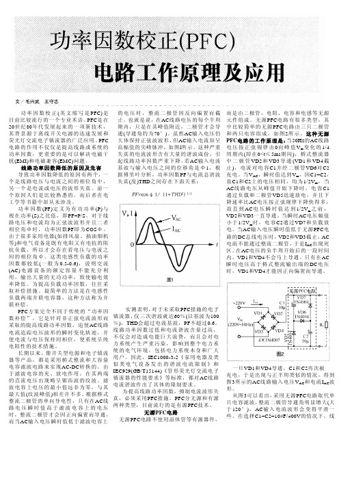
功 率 因 数 ( 是 指 交 流 输 入 有 功 功 率 ( ) 输 入 视 在 功 率 成 。其 工作 原理 简述如 下 : P与 路 输入 端 Y检 测 全波 整流 正 弦波 电压 值 , 另一 路 x是 输 出 () 比值 , S的 即: 电压 VO/ 与基 准 电压 Vrf 间 的误 差 ( 过 电压 、 差 放 大器 H e之 经 误 P — Udto  ̄一 ! c so _c ,o () 1
可 能影 响负载 的正 常工作 甚至 损坏用 电设备 ,许多 国家 都 已制 定 了限制谐波 的 国家标 准 。本 文 即讨论 了功 率因数 校 正方 案 ,讲述 U 35 C 8 4的 内部 结构 及其 工作 原 理 。 并在 此 基础 上 分析 了 U 3 5 C 84 集成 电路 的典型应 用 电路 。 1 功 率 因 数 校 正 及 控 制 方 法
原理 , U 8 4集 成 电路 的典 型 应 用 电路 作 了分 析 , 过 实 验 证 明 了 其 可 行性 和 优 越 性 。 对 C3 5 通
关键 词 : 功率 因数 ; 源 功 率 因 数 校 正 ; C35 有 U 84
随着 电力 电子 技术 的飞速 发展 和计 算机 、 讯及 I 网络 的广 通 T 泛应 用 , 大量 电力 电子装 置投 入 电网 。 电力 电子 装置 中的相 控整 流 和 不可控 二极 管整 流使输 入 电流波 形发 生严 重畸变 , 脉冲状 。 呈 电
l 很 容易 实现接 近 于 1的功率 因数 。 %,
v A M lh 1 A PK
式 中 , 表 示 输入 电压基 波有 效值 :。 , 表示 输 入 电流基 波 有 效值 ;
, 舢表 示 输 入 电流有 效值 ;
基于ICE2PCS01的有源功率因素校正的电路设计

( 西北 工 业 大 学 电 子信 息 学 院 ,陕 西 西 安 7 1 0 1 2 9 )
Hale Waihona Puke 摘要 : 针 对 开 关 电 源 中的 整 流 电路 和 其 本 身 的 非 线 性 负载 特 性 产 生 大 量谐 波 污 染 公 共 电 网 问题 . 提 出 了一 种 高功 率
( S c h o o l o fE l e c t r o n i c I n f o r m a t i o n E n g i n e e r i n g , N o r t h w e s t e r n P o l y t e c h n i c a l U n i v e r s i t y , Xi ’ 帆 7 1 0 1 2 9 , C h i n a )
第2 1卷 第 7期
V0 l _ 21
No . 7
— —
电 子 设 计 工 程
El e c t r o ni c De s i g n En g i ne e r i n g
—
2 0 1 3年 4月
Ap r .2 01 3
基于 I C E 2 P C S 0 1的有 源功率 因素校 正的 电路设计
因素 校 正 电路 。 采 用 英 飞 凌 ( I n f i n e o n ) 公 司的 C C M 控 制 模 式 功 率 因素 校 正 芯 片 I C E 2 P C S 0 1 控 制 驱 动 MO S F E T开关 管, 并 与 升压 电 感 、 输 出 电容 等 组 成 B o o s t 拓 扑 结构 。 输 入 电流 与基 准 电 流 比 较 后 的 误 差 电 流 经过 放 大 . 再与 P WM 波 比较 , 得 到 开 关 管驱 动 信 号 , 快 速 而 精 确 地使 输入 电 流 平 均值 与输 入 整 流 电压 同相 位 。 接 近正弦波。 结果表明 , 该 电路 方案能大大减小输入电流的谐波分量 , 在 A C 1 7 6 V 一 2 6 4 V 的 宽 电压 输 入 范 围 内得 到 稳 定 的 D C 3 8 0 V输 出 . 功 率 因素 高
功率因数校正电路(pfc)电路工作原理及应用
功率因数校正(英文缩写是PFC)是目前比较流行的一个专业术语。
PFC 是在20世纪80年代发展起来的一项新技术,其背景源于离线开关电源的迅速发展和荧光灯交流电子镇流器的广泛应用。
PFC 电路的作用不仅仅是提高线路或系统的功率因数,更重要的是可以解决电磁干扰(EMI)和电磁兼容(EMC)问题。
线路功率因数降低的原因及危害 导致功率因数降低的原因有两个,一个是线路电压与电流之间的相位角中,另一个是电流或电压的波形失真。
前一个原因人们是比较熟悉的。
而后者在电工学等书籍中却从未涉及。
功率因数(PF)定义为有功功率(P)与视在功率(S)之比值,即PF=P/S 。
对于线路电压和电流均为正弦波波形并且二者相位角Φ时,功率因数PF 即为COS Φ。
由于很多家用电器(如排风扇、抽油烟机等)和电气设备是既有电阻又有电抗的阻抗负载,所以才会存在着电压与电流之间的相位角Φ。
这类电感性负载的功率因数都较低(一般为0.5-0.6),说明交流(AC)电源设备的额定容量不能充分利用,输出大量的无功功率,致使输电效率降低。
为提高负载功率因数,往往采取补偿措施。
最简单的方法是在电感性负载两端并联电容器,这种方法称为并联补偿。
PFC 方案完全不同于传统的“功率因数补偿”,它是针对非正弦电流波形而采取的提高线路功率因数、迫使AC 线路电流追踪电压波形的瞬时变化轨迹,并使电流与电压保持同相位,使系统呈纯电阻性的技术措施。
长期以来,像开关型电源和电子镇流器等产品,都是采用桥式整流和大容量电容滤波电路来实现AC-DC 转换的。
由于滤波电容的充、放电作用,在其两端的直流电压出现略呈锯齿波的纹波。
滤波电容上电压的最小值远非为零,与其最大值(纹波峰值)相差并不多。
根据桥式整流二极管的单向导电性,只有在AC 线路电压瞬时值高于滤波电容上的电压时,整流二极管才会因正向偏置而导通,而当AC 输入电压瞬时值低于滤波电容上的电压时,整流二极管因反向偏置而截止。
基于BCM的有源功率因数校正电路的实现

率 变换 电路 , 功 率 因数 接 近 1 使 。有 源 功 率 因数 校
正 电路工作于高频开关状态 , 具有体积小、 重量轻 ,
收 稿 日期 : 0 2 9—1 0 0—1 1
ma e p we a trr a he 9 k o rfc o e c d 0. 9,t e s se s pe irpef r n e,e c e h e in r q ie n s h y tm u ro ro ma c r a h d t e d sg e u r me t .
关 键 词 : 源功 率 因数 校 正 ;os 变换 器 ; 界 导 电模 式 有 B ot 临
中图分类号:M 7 T 73
文献标识码 : A
文章 编 号 :4 7一( 0 0 0 93 2 1 ) 1—0 2 0 9—0 5
I p e e t to f Ac i e Po r Fa t r m l m n a i n o tv we c o
Ke r s: c ie p we a trc re to b o tc n e tr ;b u d r o u t n mo e y wo d a t o rfc o o r cin; o s o v re s o n a c nd c i d v y o
1 引言
有源 功率 因数 校正 ( c v o e at o e — A t eP w r c rC r c i F o
Co r c i n Ci c i s d o r e t r u t Ba e n BCM o
Zh S e hn
有源功率因数校正控制电路的设计

直流 电压 。 整流器 加 电容 滤波 电路 是一 种非 线性 组 件和储 能 组件 的结 合 , 因此 , 虽 然输 入交 流 电压是 正
弦的, 而输入交流 电流是一个时间很短 、 峰值很高的
周 期性 尖 峰 电流 , 波形 严重 畸 变 。 如 果去 掉输 入滤 波 电容 , 则 输 人 电流变 为 近似 的正 弦波 , 提 高 了输 入 侧 的功率 因数 并减 少 了输 入 电流 的谐波 ,但 是整 流 电
o n a d v a n c e d l i g h t p o w e r a p p l i c a t i o n , C a l T y o u t u l t r a - l o w s t a r t - u p c u r r e n t , l o w q u i e s c e n t a n d p o we r c u r r e n t . I C c o u l d w o r k i n p o we r c a v i n g mo d e . T h e d e s i g n h a s i n n e r mu l t i p l i e r , t h e o u t p u t v o l t a g e i s c o n  ̄ o H e d b y me ns a o f a
关键词 : 有源功率因数控制; 临界导电模式; 过压保护
中图分 类号 : T N 4 0 2 文献标 示 码 : A
Th e De s i g n o f c u r r e n t - mo d e P FC c o n t r o l l e r I C
NI E J i - p i n g
平 滑的直 流输 出 ,必须 在整 流 电路和 滤波 电容 之 间
一种零电压转换有源功率因数校正电路的研究
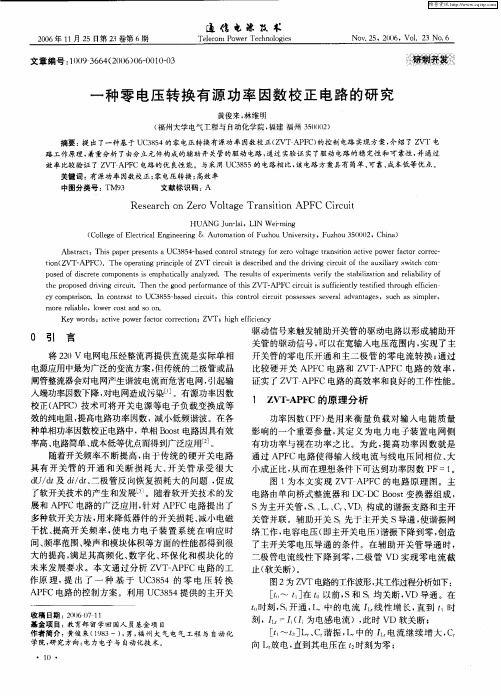
Ke r s ciep we a trc re t n VT ;hg fiin y ywo d :a t o rfco o r ci ;Z v o ih ef e c c
维普资讯
通 德 电碌 枝 】 . | =
20 0 6年 1 月 2 1 5日第 2 3卷第 6期
Teeo P we c n lge lc m o rTe h oo is No . 5 0 6,Vo.2 o. 6 v 2 ,2 0 1 3N
开关管的零电压开通和主二极管的零 电流转换; 通过 比较 硬 开 关 AP C 电路 和 Z — F 电路 的效 率 , F VT AP C 证实了 Z F VT AP C电路 的高效 率 和 良好 的工作 性 能 。
校正( P C 技术可将开关 电源等电子负载变换成等 AF) 效的纯电阻, 提高电路功率因数, 减小低频谐波。在各 种单相功率因数校正电路中, 单相 Bot os 电路因具有效 率高、 电路简单 、 成本低等优点而得到广泛应用¨。 2 ] 随着开关频率不 断提高 , 由于传统 的硬开关电路 具 有 开关 管 的 开 通 和关 断 损 耗 大 、 关 管 承 受 很 大 开 d d 及 d/ t二极 管反 向恢 复损耗 大 的问题 , 成 U/t id、 促 了软开关技术的产生和发展 。随着软开关技术 的发 展 和 AP C电路 的广 泛应用 , 对 AP C电 路提 出 了 F 针 F 多种软 开关方 法 , 用来 降低 器件 的开 关损 耗 、 小 电磁 减 干扰、 提高开关频率 , 电力电子 装置系统在 响应 时 使 间、 频率范围、 噪声和模块体积等方面的性能都得到很 大 的提 高 , 满足其 高 频 化 、 数字 化 、 环保 化 和 模 块化 的 未来 发 展要 求 。本 文 通 过分 析 Z VT— P C 电路 的工 A F 作原 理 , 出 了 一 种 基 于 UC 84 的 零 电 压 转 换 提 35 AF P C电路的控制方案。利用 U 35 C 84提供的主开关
有源功率因数校正电路设计
有源功率因数校正电路设计
有源功率因数校正电路是一种电路设计方案,用于调整电路功率因数,提高功率因数的数值。
传统的电路设备通常具有低功率因数,这会导致能
源浪费和电网负载过大。
有源功率因数校正电路的设计目的是使电路的功
率因数尽可能接近1,提高能源利用率和电力系统的稳定性。
直流母线电压检测模块用于检测直流母线的电压,并将其转化为电压
信号输出。
交流输入电压检测模块用于检测交流输入电压,并将其转化为
电压信号输出。
这两个模块的信号将作为输入信号输入到控制逻辑与驱动
模块。
这些输入信号将被控制逻辑模块分析处理,用于控制整流器和直流
-交流逆变器模块。
整流器模块的作用是将交流电转化为平滑的直流电,在此过程中,由
于非线性元件的存在,电流波形可能会出现畸变。
因此,需要使用滤波电
路对电流进行滤波,消除谐波,并将输出电流的波形调整为与输入电压同
频率的正弦波。
直流-交流逆变器模块的作用是将直流电转化为交流电,并将其输出。
为了使逆变器的工作更加稳定,需要使用滤波电路对输出电流进行滤波,
消除谐波,并将波形调整为与输入电压同频率的正弦波。
功率放大器输出滤波模块的作用是对功率放大器输出的电流波形进行
滤波,使其更加接近理想的正弦波,并消除谐波。
总的来说,设计有源功率因数校正电路需要综合运用电路和控制理论
的知识。
通过合理设计各个模块之间的关系和参数,可以实现对电路功率
因数的校正和调整,提高电路的能源利用率和稳定性。
有源功率因数校正电路设计
有源功率因数校正电路设计
首先,根据实际的电流和电压信号,使用运算放大器将信号放大到合
适的电压范围。
然后通过滤波电路对信号进行滤波,去除高频噪声。
接下来,将滤波后的信号输入到比较器中进行相位比较。
根据相位差
的方向和大小,通过控制电路的输出信号来调整功率因数。
在实际设计中,还需要考虑一些因素,以确保电路的稳定性和可靠性。
首先,选择合适的电流和电压采样电阻,以确保采样信号的准确性和稳定性。
其次,根据负载的特性和要求,选择合适的比较器和控制电路,以实
现所需的功率因数校正。
此外,还需要考虑电路的温度特性和工作环境的影响。
因为温度对电
阻和其他电子元件的性能有很大影响,所以在设计过程中需要采取适当的
温度补偿措施。
此外,还需要考虑电路的成本和功耗。
根据实际需求,选择合适的元
件和电路结构,以降低成本和功耗。
总之,有源功率因数校正电路的设计需要综合考虑电路的原理和性能
要求,以及实际应用的需求和经济因素。
只有在充分理解电路原理的基础上,才能设计出稳定可靠、性能优良的有源功率因数校正电路。
采用UC3854的有源功率因数校正电路工作原理与应用
采用UC3854的有源功率因数校正电路工作原理与应用北京信息职业技术学院 100031 路秋生简介:本文主要介绍了有源功率因数校正(APFC)的工作原理、电路分类。
并对在国内得到广泛应用的UC3854集成电路的典型应用电路、工作原理做了介绍、分析。
关键词:功率因数(PF)有源功率因数校正乘法器除法器一.功率因数校正原理1.功率因数(PF)的定义功率因数(PF)是指交流输入有功功率(P)与输入视在功率(S)的比值。
即所以功率因数可以定义为输入电流失真系数()与相移因数()的乘积。
可见功率因数(PF)由电流失真系数()和基波电压、基波电流相移因数()决定。
低,则表示用电电器设备的无功功率大,设备利用率低,导线、变压器绕组损耗大。
同时,值低,则表示输入电流谐波分量大,将造成输入电流波形畸变,对电网造成污染,严重时,对三相四线制供电,还会造成中线电位偏移,致使用电电器设备损坏。
由于常规整流装置常使用非线性器件(如可控硅、二极管),整流器件的导通角小于180o,从而产生大量谐波电流成份,而谐波电流成份不做功,只有基波电流成份做功。
所以相移因数()和电流失真系数()相比,输入电流失真系数()对供电线路功率因数(PF)的影响更大。
为了提高供电线路功率因数,保护用电设备,世界上许多国家和相关国际组织制定出相应的技术标准,以限制谐波电流含量。
如:IEC555-2, IEC61000-3-2,EN 60555-2等标准,它们规定了允许产生的最大谐波电流。
我国于1994年也颁布了《电能质量公用电网谐波》标准(GB/T14549-93)。
传统的功率因数概念是假定输入电流无谐波电流(即I1=I rms或=1)的条件下得到的,这样功率因数的定义就变成了PF =。
二.PF与总谐波失真系数(THD:The Total Harmonic Distortion)的关系三.功率因数校正实现方法由功率因数可知,要提高功率因数,有两个途径:1.使输入电压、输入电流同相位。
开关电源的有源功率因数校正电路设计
家人 网电气 设备 的电 流谐 波值 进行 了限制 ,严 格 限定 设 备 的 功率 因数 必 须 接 近于 1,所 以 ,提 高 开 关 电源 的功 率 因数 已经 成 为 国内 电源 厂商 的 当务 之急 。
由于输入端 有整流元 件和滤 波 电容 ,单相 AC/DC开关 电源及大部分整流 电源供电的电子设 备 ,其电网侧功率 因数仅为 0.65左右 。采用有源 功率 校 正技 术 后 可提 高 到 0.99以上 ,既 治理 了 电 网的谐波污染 ,又提高了开关 电源的整体效率。有 源 功 率 因数 校 正 主 要 是 在 整 流 滤 波 和 DC/DC功 率级之 间串人一个有源 PFC作为前置级 ,用来提 高功率因数和实现 DC/DC级输入的预稳 ,PFC电
中图分 类号 :TN86 文献 标识 码 :A 文 章编 号 :0219—2713(2007)10—0013—05
0 引 言
近 年来 ,由于 开 关 电源效 率 高 ,成 本 低 ,而在 各个领域获得了广泛的应用 。但是采用传统的非 控整流开关 电源 ,由于输入阻抗呈容性 ,网侧输入 电压和 输入 电流 间存 在 较 大相 位差 ,加 上 输入 电 流严重非正弦 ,并呈脉冲状 ,故功率 因数极低(在 0.65左右 ),谐波成分很大 ,给 电力系统 带来 了严 重 的谐 波 污 染 。 为此 ,国 际 上 推 行 了 IEC5552、 EN60555—2、IEEE—Std一519等标 准对电子生产厂
(1.Zhejiang Provincial Plan Design& Research Institute of Communications, Hangzhou Zhejiang 3 10006, China)
- 1、下载文档前请自行甄别文档内容的完整性,平台不提供额外的编辑、内容补充、找答案等附加服务。
- 2、"仅部分预览"的文档,不可在线预览部分如存在完整性等问题,可反馈申请退款(可完整预览的文档不适用该条件!)。
- 3、如文档侵犯您的权益,请联系客服反馈,我们会尽快为您处理(人工客服工作时间:9:00-18:30)。
Active Power Factor Correction(PFC)Circuit With Resistor-Free Zero-Current Detection Yong-Seong Roh,Young-Jin Moon,Jung-Chul Gong,and Changsik Yoo,Member,IEEEAbstract—An active power-factor correction(PFC)circuit is presented that employs a newly proposed resistor-free zero-current detection(ZCD).While the conventional ZCD requires either a sensing resistor or auxiliary transformer,the proposed ZCD re-quires only one OFF-chip capacitor.The active PFC circuit with the proposed resistor-free ZCD has been implemented in a0.35-μm BCDMOS process and the power factor is improved up to9%from the one employing the conventional ZCD.The proposed resistor-free ZCD scheme can be applied to any type of switch-mode dc–dc power converter.Index Terms—Critical conduction mode(CRM),discontinuous conduction mode(DCM),power-factor correction(PFC),zero-current detection(ZCD).I.I NTRODUCTIONP OWER factor(PF)is defined as the ratio of real power to apparent power,where real power produces real work and apparent power is the total power that a power company has to supply[1].When PF is not100%,the current waveform does not follow the voltage waveform.This results in power losses and may also cause harmonics that travel down the neutral line and disrupt other devices connected to the line[1],[2].The power-factor-correction(PFC)circuit basically shapes the input current waveform to be the replica of the input voltage waveform and exactly in phase with it.Active PFC is preferred to passive one because of its small form factor and much better PF.Active PFC is usually based on a boost converter where the feedback control can be performed in either continuous conduction mode(CCM),discontinuous con-duction mode(DCM),or critical conduction mode(CRM)[3]. Converter that operates in CCM induces small device current stress and the requirement on inputfilter is relaxed.However, the hard turn-OFF of freewheeling diode increases power lossManuscript received February8,2010;revised April22,2010and June29, 2010;accepted August6,2010.Date of current version February11,2011. This work was supported by the Basic Science Research Program through the National Research Foundation of Korea(NRF)funded by the Ministry of Educa-tion,Science,and Technology under Grant2010–0012551,and by the Samsung Power IC Design(SPID)Center,University of Seoul,Korea.The CAD tools were provided by IDEC.Recommended for publication by Associate Editor J.A.Pomilio.Y.-S.Roh,Y.-J.Moon,and C.Yoo are with the Integrated Circuits Laboratory, Hanyang University,Seoul133–791,Korea(e-mail:amyung@hanyang.ac.kr; worthforj@;csyoo@hanyang.ac.kr).J.-C.Gong is with the Integrated Circuits Laboratory,Hanyang University, Seoul133–791,Korea,and also with Samsung Electro-Mechanics,Suwon 442-743,Korea(e-mail:jungchul.gong@).Color versions of one or more of thefigures in this paper are available online at .Digital Object Identifier10.1109/TPEL.2010.2070080Fig.1.Conventional ZCD techniques.(a)With a sensing resistor R C S.(b)With an auxiliary transformer.and switching noise.DCM is commonly used for low-powerapplication.Freewheeling diode is turned off softly and switchis turned on at zero current,providing high efficiency.CRM thatoperates at the boundary between CCM and DCM has interme-diate characteristics.Both DCM and CRM are often combinedto exploit the advantages of each mode.When downstream con-verter requires large output power,CRM is selected to reducepeak inductor current.When low output power is required,DCMis used to reduce switching frequency for higher efficiency[4].For DCM and CRM operation,the instant when inductor cur-rent becomes zero has to be detected by a zero-current-detection(ZCD)circuit.The simplest way of detecting the instant when the inductorcurrent I L becomes zero is to insert a sensing resistor in serieswith the inductor and sense the voltage drop across it[5].Sincesilicon process technologies allow only limited voltage stresson active devices,it is safer to place a sensing resistor R CSon the ground line,as shown in Fig.1(a).This incurs a powerloss and noise on the ground line,decreasing the efficiency andachievable PF.If an auxiliary transformer is used,as shownin Fig.1(b),the voltage induced in the secondary winding is 0885-8993/$26.00©2010IEEEFig.2.PFC circuit with resistor-free ZCD.The components in the shaded regions are off-chip.utilized to sense the zero current of the primary winding,and the power loss due to sensing resistor can be avoided[6].However, the auxiliary transformer increases the form factor and cost. There have been lots of alternative approaches to overcome the aforementioned issues of the conventional ZCD schemes [7],[18].By monitoring the inductor voltage,ZCD can be per-formed[7],but it cannot be applied to PFC because the inductor voltage may be extremely large in PFC and active devices for ZCD can be exposed to severe voltage stress.Based on the relationship between inductor current and voltage,the input line current can be sensed by monitoring the input and output voltages[8],[9],but high-performance digital signal process-ing(DSP)is required.The optimum duty cycle of switching clock can be stored in memory to remove current sensor[10], but to be operable in universal condition,huge amount of data have to be stored.Lee and Lim implemented a three-phase pulsewidth modulation(PWM)rectifier with a current sensor on ground line[11].The input line current is reconstructed using the sensed ground line current and switching states of the PWM rectifier,but this cannot be applied to a single-phase PFC converter.In[12],the current through switch transistor is sensed with a sensing resistor instead of inductor current. In[13]–[18],techniques for removing current sensor and/or voltage sensor are described.With the technique in[13],PF can be greatly degraded in the presence of harmonic components in the input voltage.Fast DSP is required to implement the scheme in[14].The scheme in[15]requires extremely large RC time constant to implement a differentiator and envelop detec-tor.In[16]and[17],the output current is predicted from digital data streams of digitally controlled electronic load in dc–dc con-verters,and therefore,this scheme cannot be used for general applications.In[18],current sensor is removed by employing a phase shifter,but the improvement of PF is limited under various load conditions.In this paper,a new ZCD is proposed where the instant of zero inductor current is detected by monitoring the input andoutput Fig.3.Waveform of the inductor current in DCM and CRM.In CRM t3is zero.voltage instead of inductor current or voltage.The proposed scheme does not require any sensing resistor,and therefore,is called resistor-free ZCD.For resistor-free ZCD,only one exter-nal capacitor is additionally required.In Section II,the opera-tion principle is explained and its implementation detail is given in Section III.The experimental results follow in Section IV, andfinally,Section V concludes this paper.II.R ESISTOR-F REE ZCD T ECHNIQUEFig.2shows the active PFC circuit employing the proposed resistor-free ZCD technique.The resistor-free ZCD circuit de-tects the instant of zero inductor current by monitoring input and output voltages.The bandgap reference provides an accurate reference voltage level with which the resistor-divided output voltage V out div is compared to generate the error voltage V err. Fig.3shows the waveform of the inductor current in DCM and CRM,where t3is zero in CRM.Ignoring the voltage drop across the diode D1,the voltage across the inductor is V in and V in−V out when the power switch M N is turned on and off,Fig.4.(a)Resistor-free ZCD circuit where the capacitor C1is off-chip and (b)multiplied by two circuits.respectively.Therefore,t1and t2are related with each other ast2=V inV out−V int1.(1)If V in and V out are known,t2is predictable because t1is the internally generated timing.The inductor current is zero at t= t1+t2and the instant of zero inductor current is predictable. Since the switching frequency for PFC control is much higher than the frequency of the input line voltage,the rectified line voltage V in can be safely assumed to be dc.III.I MPLEMENTATIONA.Resistor-Free ZCD CircuitThe resistor-free ZCD circuit is very simple as shown in Fig.4(a).The signalΦ1is the gate-driving signal of the power switch M N.WhenΦ1is high,the capacitor C1is charged by the current source I1that is designed to be V in div/R B,where V in div is the scaled input voltage,as shown in Fig.2.The voltage V C1across C1is amplified by the multiply-by-two circuit in Fig.4(b)to get V C2.At t=t1,V C1is I1t1/C1,and therefore, V C2is2I1t1/C1,which is held on C2whileΦ1is low.WhenΦ1 is low,C1is charged by I2,which is(V out div−V in div)/R B, where V out div is the scaled output voltage,as shown in Fig.2. The output of the comparator is high when V C1becomes larger than V C2.At this instant,V C1is given asV C1=I1t1C1+I2t 2C1=2I1t1C1(2) and t2can be rearranged ast 2=I1t1I2=V in div/R B(V out div−V in div)/R Bt1.(3)If the resistance ratios R1/R2and R3/R4of the input and output voltage dividers of Fig.2are equal to each other,t 2is given ast 2=V inV out−V int1.(4) We can see that t 2in(4)is equal to t2in(1),and therefore, when the comparator output V comp becomes high and dead time (DT)is set to high,the inductor current is zero.The timing of the resistor-free ZCD circuit is shown in Fig.5.The additional advantage of the resistor-free ZCD circuit, shown in Fig.4(a),is the overcurrent protection(OCP)that can be performed without a sensing resistor by detecting V C1during t1because V C1is proportional to the input line current during t1.However,the current chip does not utilize this feature,and a sensing resistor is inserted between the source of M N and ground in Fig.2for OCP.In the conventional ZCD scheme employing a sensing resistor on the ground line,the magnitude of the sensing resistor should be small to avoid substantial power loss.However,near the zero-current condition,the current level is very small and the ZCD with small sensing resistance can be very susceptible to noise.In the proposed resistor-free ZCD,the sensing resistor inserted between the source of M N and ground is to detect overcurrent condition.Therefore,even with small sensing resistance,OCP is rather immune to noise.B.Current Generator for I1and I2For proper operation of the resistor-free ZCD,the currents I1and I2are precisely generated by the current generator shown in Fig.6.The currents through the transistors M1and M2are regulated to be V in div/R B and V out div/R B,respec-tively,by gain-boosted cascode stages.The current through M1 is copied to the transistor M20that provides the current out-put I1=V in div/R B.The current through M2is copied to the transistor M11from which V in div/R B is subtracted to have cur-rent(V out div−V in div)/R Bflow through the transistor M18, which provides the current output I2.In order to improve the matching property between the two resistors,dummy resistors are used and the common centroid layout technique is applied.The phase margin of the feedback loop composed of A1,M1,and R B(A2,M2,and R B)is81◦, while the loop gain is60dB and the unity gain frequency is 32MHz.C.V tO NProcessing CircuitFrom Fig.3,the average input current can be calculated asI in,avg=t1(t1+t2)V in2LT.(5)Fig.5.Timing diagram of resistor-free ZCD in(a)DCM and(b)CRM.If PFC operates in CRM where t1+t2=T,the average input current is proportional to the input voltage for constant t1,and thus,PF is properly corrected.However,in DCM,the aforementioned statement does not apply,and from(1),the average input current can be expressed asI in,avg=t21V in V out2LT(V out−V in).(6)It is clear that the average input current is not proportionalto V in and the harmonics may be present in the input current,resulting in poor PF.In order to improve PF in DCM,the errorvoltage V err is postprocessed with the V tO Nprocessing circuit[5].The V tO Nprocessing circuit is redrawn in Fig.7(a)and itstiming diagram is shown in Fig.7(b).Assuming the operationalamplifier to be ideal,the following relationship holds:V x−V errR p1=C p1d(V err−V y)dt.(7)Since the error voltage V err in Fig.2is nearly dc,the slope ofV y is given asdV ydt=V err−V xR p1C p1.(8)When DT is low,V x is equal to V y and V y is discharged asmuch asΔV y|D T=low=−t1+t2dV y=−1R p1C p1t1+t2(V err−V y)dt.(9)Since the time constant R p1C p1in Fig.7(a)is set to be muchlarger than the clock period T,it can be safely assumed that V y isdischarged linearly when DT is low.Then,(9)can be rearrangedasΔV y|D T=low=−t1+t2R p1C p1V err−V y,min−ΔV y|D T=low2.(10)When DT is high(zero inductor current),V x is0V and V y ischarged as much asΔV y|D T=high=t1+t2+t3t1+t2dV y=V err t3R p1C p1.(11)Since the net change of V y during one period T should be zeroin the steady stateΔV y=ΔV y|D T=low=ΔV y|D T=high(12)andV err=t1+t2TV y,min+ΔV y2.(13)The average value of V y can be calculated asV y,avg=V y,min+12ΔV y(14)and from(13)V y,avg=Tt1+t2V err.(15)For further suppression of the ripple in V y,additional low-passfilter,composed of R p2and C p2,is used,and the outputV tO Nof the low-passfilter is equal to the average value of V yV tO N=T(t1+t2)V err.(16)Fig.6.Current generator for I 1and I 2of the resistor-free ZCD circuit shown in Fig.4(a).Fig.7.(a)V t O N processing circuit and (b)its timing diagram.If the slope of the ramp signal is S ,the high pulsewidth t 1of Φ1is V t O N /S and the average input current isI in ,avg =V err2LS×V in(17)that is proportional to the input line voltage.Therefore,we can achieve good PF both in CRM and DCM.D.Clock and Ramp GeneratorThe clock and ramp generator shown in Fig.8(a)is used for PWM (PWM)control.The current through M 2charges the capacitor C t and when V G 4becomes high ,the transistor M 4turns on and discharges the capacitor C t .The ON-resistanceFig.8.(a)Clock and ramp generator and its timing diagram in (b)DCM and (c)CRM.Fig.9.Microphotograph of the PFC circuit.of the transistor M4is designed to be small enough to fully discharge the capacitor C t.In order to support both DCM and CRM,the ZCD signal DT is AND-gated with the SR-latch output Q latch.If the inductor current becomes zero(DT=high)before the ramp signal V ramp reaches V H,as shown in Fig.8(b),the clock signal CLK hasfixed frequency determined as V ref/V H C t R t and the PFC operates in DCM.In Fig.8(c),the inductor current becomes zero(DT= high)after the ramp signal V ramp becomes larger than V H. Then,the clock signal CLK is synchronized to DT and the PFC operates in CRM.It should be noted,as shown in Fig.8(b)and (c),that pulse DT always occurs before the CLK pulse.Due to use of the delay line D T in Fig.8(a)whose nominal delay is 100ns,the interval from the DT pulse to the next switching cycle is100ns when the PFC operates in CRM.By adding a capacitor across the power switch M N in Fig.2, the resonant frequency at the drain node of M N can be adjusted; therefore,the next switching cycle begins when the drain node voltage is zero,achieving valley switching.IV.E XPERIMENTAL R ESULTSThe PFC circuit has been implemented in a0.35-μm BCDMOS process and its microphotograph is shown in Fig.9. The area of the whole chip is2.03mm2.The PFC circuit is designed so that it can select one between the conventional ZCD with a sensing resistor and the proposed resistor-free ZCD.The conventional ZCD with a sensing resistor includesthe V tO N processing circuit as well,and its sensing resistor is0.1Ω.For performance comparison with the conventional ZCD scheme using an auxiliary transformer,the commercial PFC controller IC,FAN7530,is used to implement a PFC circuit, while the same power stage is utilized as for the proposed ZCD scheme[6].The PFC circuit provides390-V dc output from ac input line voltage of85–267V rms.The maximum outputcurrent Fig.10.Measured PF when the input line voltage is(a)100V rm s, (b)150V rm s,(c)200V rm s,and(d)230V rm s.is500mA,while6mA is dissipated internally for the operation of the PFC controller.In Fig.10,the measured PF is shown for the input line voltage of100,150,200,and230V rms.As can be seen in thefigure,the proposed resistor-free ZCD can improve PF by up to9%from the one using a sensing paring the ZCD with an auxiliary transformer,the proposed resistor-free ZCD shows similar or better PF.The performance of the implemented PFC circuit employing the proposed resistor-free ZCD scheme is summarized in Table I.TABLE IP ERFORMANCE SUMMARYV .C ONCLUSIONThe inductor current of active PFC circuit is monitored by the resistor-free ZCD.The resistor-free ZCD requires only one off-chip capacitor,and therefore,can provide much smaller form factor than the conventional ZCD schemes.The PFC circuit employing the proposed resistor-free ZCD is implemented in a 0.35-μm BCDMOS process and PF is improved up to 9%from the one employing the conventional ZCD.The proposed resistor-free ZCD scheme can be applied to any type of switch-mode dc–dc power converter.A CKNOWLEDGMENTThe authors would like to thank Prof.J.Choi and Prof.K.-C.Kim of University of Seoul,Korea and Prof.K.-Y .Lee of Konkuk University,Seoul for their help during this study.The CAD tools were provided by the IC Design Education Center (IDEC).R EFERENCES[1]Power Factor Correction Basics,Application Note 42047,Fairchild Semi-conductor,South Portland,ME,2004.[2]Power Factor Correction Handbook,ON Semiconductor,Phoenix,AZ,Sep.2007.[3]R.W.Erickson and D.Maksimovic,Fundamental of Power Electronics ,2nd ed.Boston,MA:Kluwer,2001,pp.609–630.[4]L.Huber,B.T.Irving,and M.M.Jovanovic,“Effect of valley switch-ing and switching-frequency limitation on line-current distortions of DCM/CCM boundary boost PFC converters,”IEEE Trans.Power Elec-tron.,vol.24,no.2,pp.339–347,Feb.2009.[5]Data Sheet of NCP 1605,ON Semiconductor,Phoenix,AZ,2009.[6]Data Sheet of FAN 7530,Fairchild Semiconductor,South Portland,ME,Apr.2006.[7]H.-P.Le,C.-S.Chae,M.-C.Lee,S.-W.Wang,S.-I.Kim,and G.-H.Cho,“Integrated zero-inductor-current detection circuit for step-up DC-DC converters,”IET Electron.Lett.,vol.42,no.16,pp.943–944,Aug.2006.[8]S.Sivakumar,K.Natarajan,and R.Gudelewicz,“Control of power factorcorrecting boost converter without instantaneous measurement of input current,”IEEE Trans.Power Electron.,vol.10,no.4,pp.435–445,Jul.1995.[9]S.Bhowmik,A.van Zyl,R.Spee,and J.H.R.Enslin,“Sensorless currentcontrol for active rectifiers,”IEEE Trans.Ind.Appl.,vol.33,no.3,pp.765–773,May/Jun.1997.[10] A.Garcia,A.de Castro,O.Garcia,and F.J.Azcondo,“Pre-Calculatedduty cycle control implemented in FPGA for power factor correction,”in Proc.35th Annu.Conf.IEEE Ind.Electron.(IECON’2009),pp.2955–2960.[11] D.C.Lee and D.S.Lim,“AC voltage and current sensorless control ofthree-phase PWM rectifiers,”IEEE Trans.Power Electron.,vol.17,no.6,pp.883–890,Nov.2002.[12]J.Sun and M.Chen,“Nonlinear average current control using partialcurrent measurement,”IEEE Trans.Power Electron.,vol.23,no.4,pp.1641–1648,Jul.2008.[13]T.Ohnishi and M.Hojo,“DC voltage sensorless single-phase PFC con-verter,”IEEE Trans.Power Electron.,vol.19,no.2,pp.404–410,Mar.2004.[14]T.Noguchi,H.Tomiki,S.Kondo,and I.Takahashi,“Direct power controlof PWM converter without power-source voltage sensors,”IEEE Trans.Ind.Appl.,vol.34,no.3,pp.473–479,May/Jun.1998.[15] D.Y .Qiu,S.C.Yip,H.S.H.Chung,and S.Y .Ron Hui,“Single currentsensor control for single-phase active power factor correction,”IEEE Trans.Power Electron.,vol.17,no.5,pp.623–632,Sep.2002.[16]S.Chae,B.Hyun,P.Agarwal,W Kim,and B.Cho,“Digital predictivefeed-forward controller for a DC-DC converter in plasma display panel,”IEEE Trans.Power Electron.,vol.23,no.2,pp.627–634,Mar.2008.[17]O.Trescases,G.Wei,A.Prodic,and W.T.Ng,“Predictive efficiencyoptimization for DC-DC converters with highly dynamic digital loads,”IEEE Trans.Power Electron.,vol.23,no.4,pp.1859–1869,Jul.2008.[18]H.Chen,“Duty phase control for single-phase boost-type SMR,”IEEETrans.Power Electron.,vol.23,no.4,pp.1927–1934,Jul.2008.Yong-Seong Roh received the B.S.(with the highest honors)degree in electrical and computer engineer-ing,in 2007,from Hanyang University,Seoul,Korea,where he is currently working toward the Ph.D.degree.His current research interests include power-management ICdesign.Young-Jin Moon received the B.S.degree in electri-cal and computer engineering,in 2008,from Hanyang University,Seoul,Korea,where he is currently work-ing toward the Ph.D.degree.His current research interests include power-management IC design.Jung-Chul Gong received the B.S.degree in elec-tronics from Kwangwoon University,Seoul,Korea, in2000,and is currently working toward the M.S. degree in electrical and computer engineering from Hanyang University,Seoul.He joined Samsung Electro-Mechanics,Suwon, Korea,in2000,where he is currently a Senior De-sign Engineer.His research interests include power-management ICdesign.Changsik Yoo(S’92–M’00)received the B.S.(withthe highest honors),M.S.and Ph.D.degrees in elec-tronics engineering from Seoul National University,Seoul,Korea,in1992,1994,and1998,respectively.From1998to1999,he was a Member of Re-search Staff at Integrated Systems Laboratory(IIS),Swiss Federal Institute of Technology(ETH),Zurich,Switzerland,where he was involved in the researchon CMOS RF circuits.From1999to2002,he was atSamsung Electronics,Hwasung,Korea.Since2002,he has been an Associate Professor at Hanyang Uni-versity,Seoul.His research interests include CMOS RF transceiver design, mixed-mode CMOS circuit design,high-speed interface circuit design,and power-management IC design.Dr.Yoo is the winner or co-winner of several technical awards including the Samsung Best Paper Bronze Award in2006International SoC Design Confer-ence,the Silver Award in2006IDEC Chip Design Contest,the Best Paper Award in2006Silicon RF IC Workshop,and the Golden Prize for research achievement in the next-generation DRAM design from Samsung Electronics in2002.He is a member of the technical committee of IEEE International Solid-State Circuits Conference(ISSCC),the Very Large Scale Integration(VLSI)Circuits Sympo-sium(SOVC),and the European Solid-State Circuits Conference(ESSCIRC).。